The Electronic Properties of O-Doped Pure and Sulfur Vacancy-Defect Monolayer WS2: A First-Principles Study


Abstract
:1. Introduction
2. Physical Modeling and Simulation Methods
3. Results and Discussion
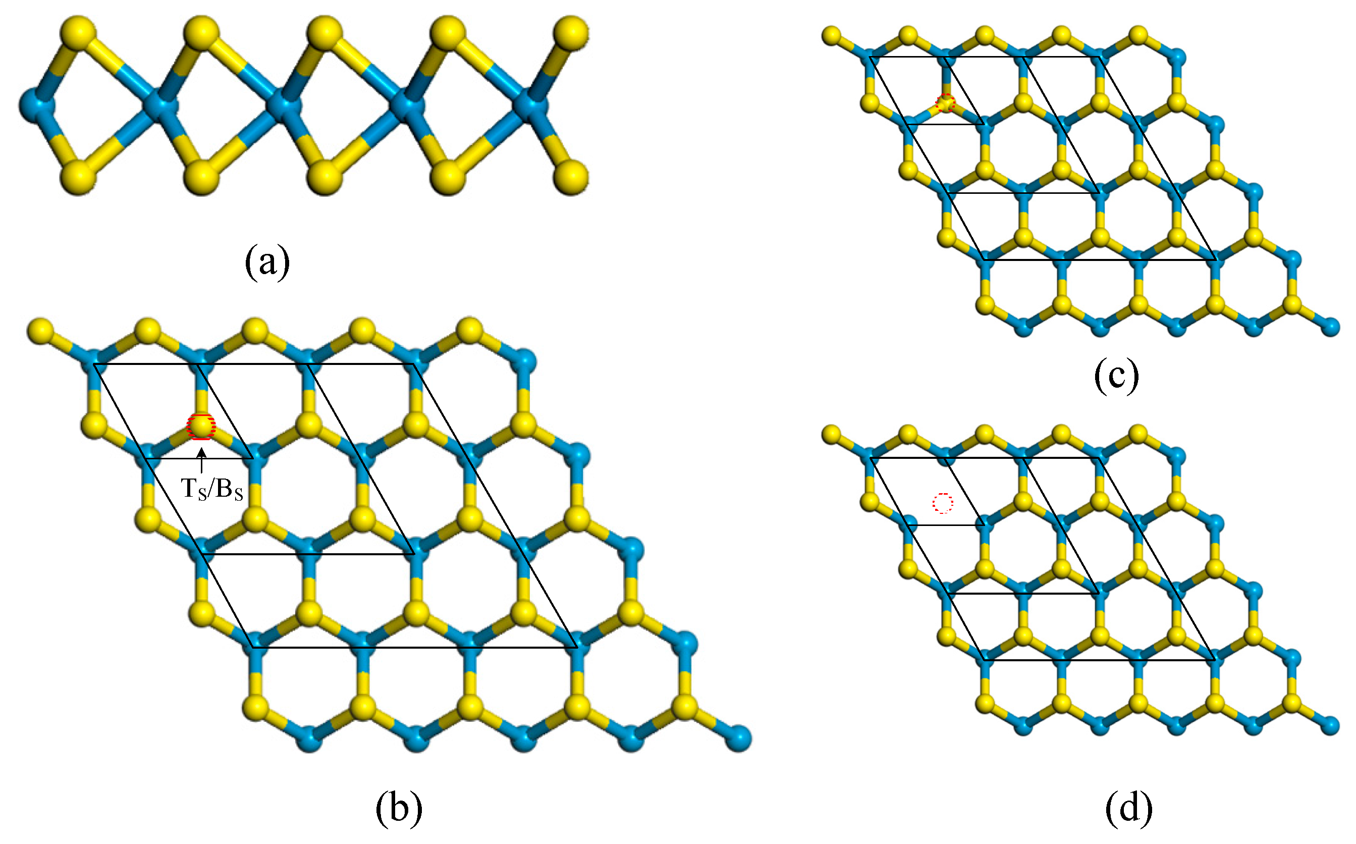
3.1. Structure Properties
3.2. Band Structure and Density of States (DOS)
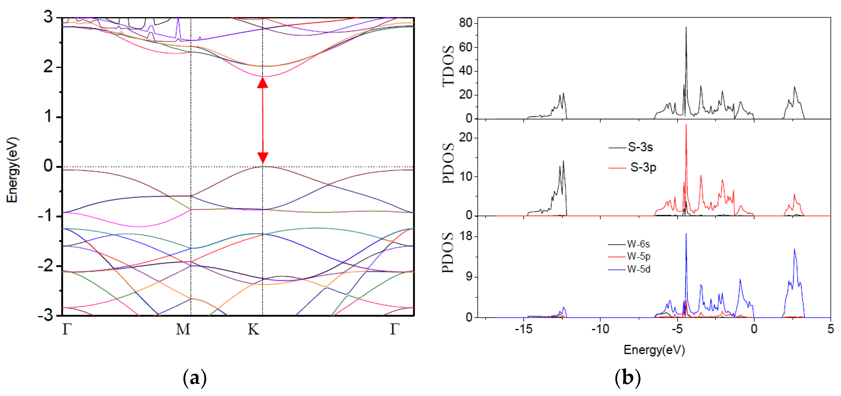
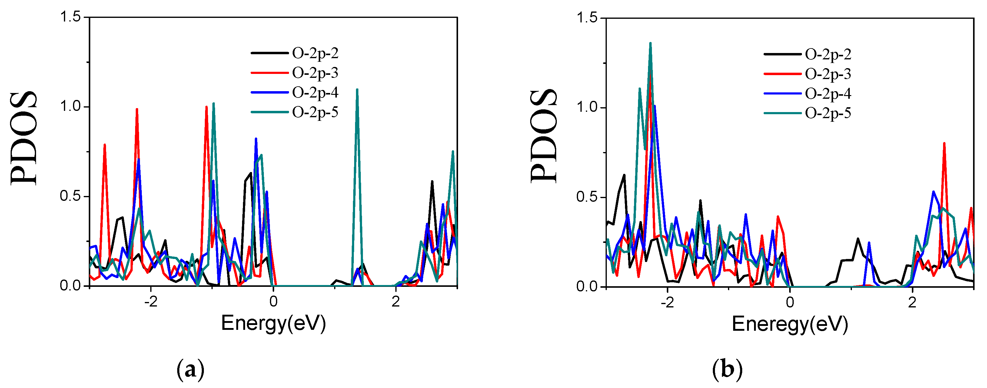
3.2.1. O-Doped Pure WS2
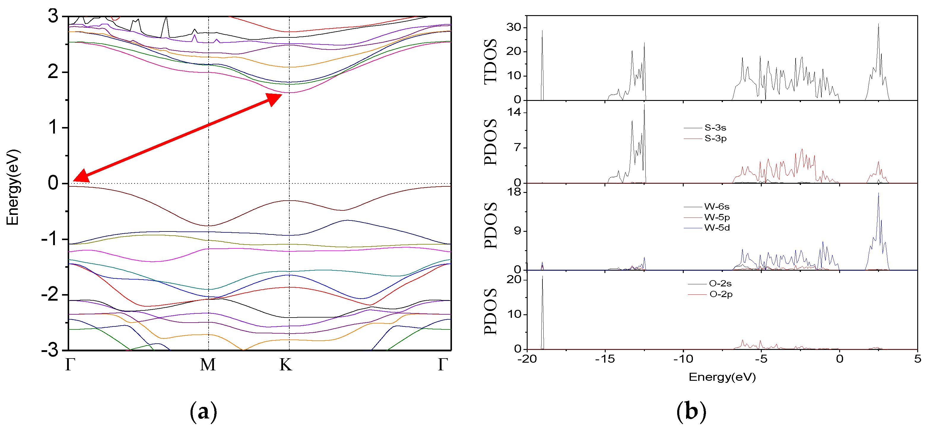
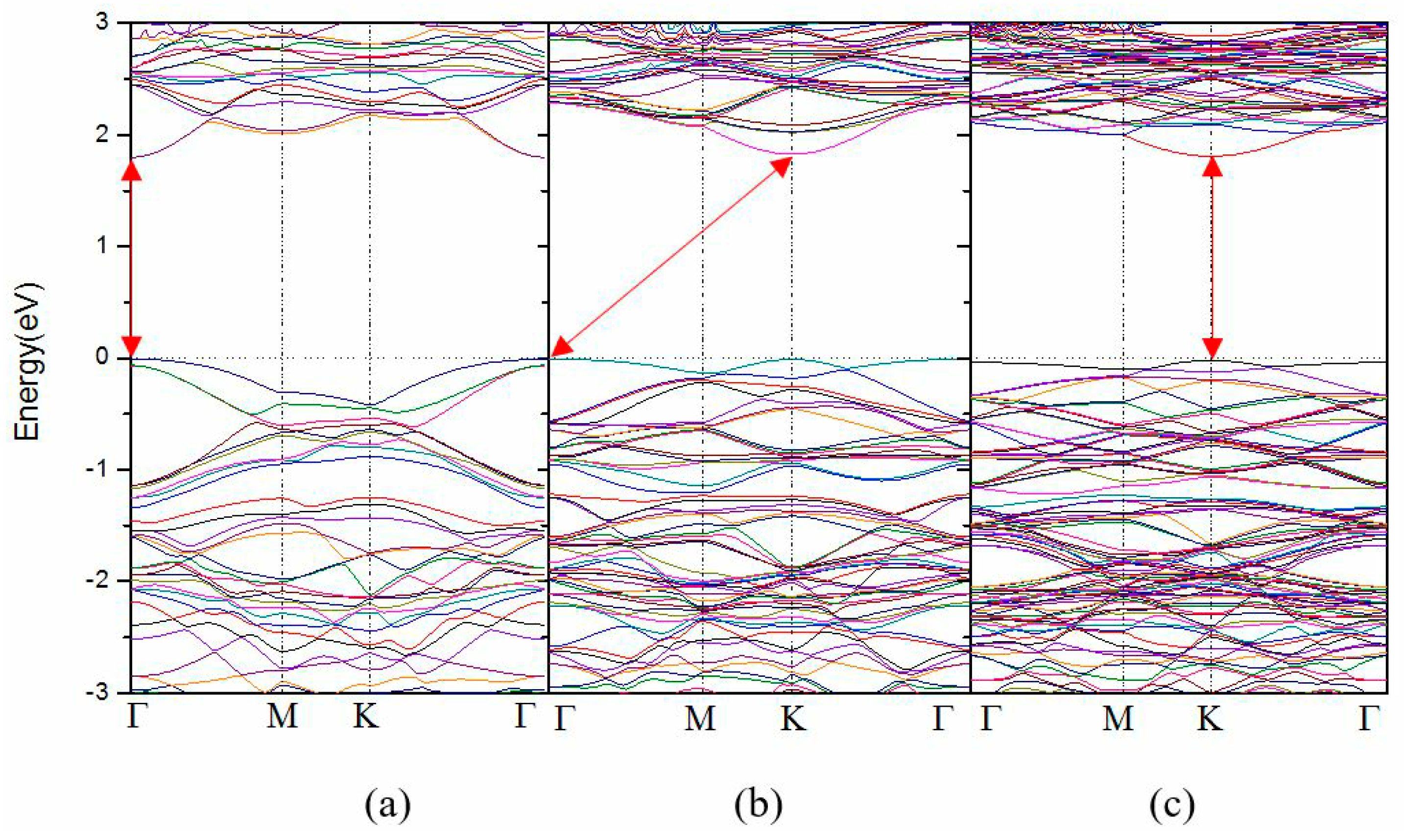
3.2.2. O-Doped Sulfur Vacancy-Defect WS2
4. Conclusions
Acknowledgments
Author Contributions
Conflicts of Interest
References
- Georgiou, T.; Yang, H.; Jalil, R.; Chapman, J.; Novoselov, K.S.; Mishchenko, A. Electrical and optical characterization of atomically thin WS2. Dalton Trans. 2014, 43, 10388–10391. [Google Scholar] [CrossRef] [PubMed]
- Zhao, W.; Ghorannevis, Z.; Chu, L.; Toh, M.; Kloc, C.; Tan, P.; Eda, G. Evolution of Electronic Structure in Atomically Thin Sheets of WS2 and WSe2. ACS Nano 2012, 7, 791–797. [Google Scholar] [CrossRef] [PubMed]
- Zeng, Z.; Yin, Z.; Huang, X.; Li, H.; He, Q.; Lu, G.; Boey, F.; Zhang, H. Single-layer semiconducting nanosheets: High-yield preparation and device fabrication. Angew. Chem. Int. Ed. 2011, 50, 11093–11097. [Google Scholar] [CrossRef] [PubMed]
- Peimyoo, N.; Yang, H.; Shang, J.; Shen, X.; Wang, Y.; Yu, H. Chemically Driven Tunable Light Emission of Charged and Neutral Excitons in Monolayer WS2. ACS Nano 2014, 8, 11320–11329. [Google Scholar] [CrossRef] [PubMed]
- Peimyoo, N.; Shang, J.; Cong, C.; Shen, X.; Wu, X.; Yeow, E.; Yu, T. Nonblinking, Intense Two-Dimensional Light Emitter: Monolayer WS2 Triangles. ACS Nano 2013, 7, 10985–10994. [Google Scholar] [CrossRef] [PubMed]
- Thripuranthaka, M.; Late, D.J. Temperature dependent phonon shifts in single-layer WS2. ACS Appl. Mater. Interfaces 2014, 6, 1158–1163. [Google Scholar]
- Jo, S.; Ubrig, N.; Berger, H.; Kuzmenko, A.B.; Morpurgo, A.F. Mono- and bilayer WS2 light-emitting transistors. Nano Lett. 2014, 14, 2019–2025. [Google Scholar] [CrossRef] [PubMed]
- Ovchinnikov, D.; Allain, A.; Huang, Y.; Dumcenco, D.; Kis, A. Electrical Transport Properties of Single-Layer WS2. ACS Nano 2014, 8, 8174–8181. [Google Scholar] [CrossRef] [PubMed]
- Mahler, B.; Hoepfner, V.; Liao, K.; Ozin, G.A. Colloidal Synthesis of 1T-WS2 and 2H-WS2 Nanosheets: Applications for Photocatalytic Hydrogen Evolution. J. Am. Chem. Soc. 2014, 136, 14121–14127. [Google Scholar] [CrossRef] [PubMed]
- Rapoport, L.; Fleischer, N.; Tenne, R. Fullerene-like WS2 Nanoparticles: Superior Lubricants for Harsh Conditions. Adv. Mater. 2003, 15, 651–655. [Google Scholar] [CrossRef]
- Zhao, X.; Xia, C.; Dai, X.; Wang, T.; Chen, P.; Tian, L. Electronic and magnetic properties of X-doped (X = Ni, Pd, Pt) WS2 monolayer. J. Magn. Magn. Mater. 2016, 414, 45–48. [Google Scholar] [CrossRef]
- Chanana, A.; Mahapatra, S. Density functional theory based study of chlorine doped WS2-metal interface. Appl. Phys. Lett. 2016, 108, 103107. [Google Scholar] [CrossRef]
- Wei, J.; Ma, Z.; Zeng, H.; Wang, Z.; Wei, Q.; Peng, P. Electronic and optical properties of vacancy-doped WS2 monolayers. AIP Adv. 2012, 2, 042141. [Google Scholar] [CrossRef]
- Chen, W.; Zhao, J.; Zhang, J.; Gu, L.; Yang, Z.; Li, X.; Yu, H.; Zhu, X.; Yang, R.; Shi, D.; et al. Oxygen-Assisted Chemical Vapor Deposition Growth of Large Single-Crystal and High-Quality Monolayer MoS2. J. Am. Chem. Soc. 2015, 137, 15632–15635. [Google Scholar] [CrossRef] [PubMed]
- Coleman, J.N.; Lotya, M.; O’Neill, A.; Bergin, S.D.; King, P.J.; Khan, U.; Young, K.; Gaucher, A.; De, S.; Smith, R.J.; et al. Two-Dimensional Nanosheets Produced by Liquid Exfoliation of Layered Materials. Science 2011, 331, 568–571. [Google Scholar] [CrossRef] [PubMed]
- Matte, H.S.S.R.; Gomathi, A.; Manna, A.K.; Late, D.J.; Datta, R.; Pati, S.K.; Rao, C.N.R. MoS2 and WS2 Analogues of Graphene. Angew. Chem. Int. Ed. 2010, 49, 4059–4062. [Google Scholar] [CrossRef] [PubMed]
- Gutiérrez, H.R.; Perea-López, N.; Elías, A.L.; Berkdemir, A.; Wang, B.; Lv, R.; López-Urías, F.; Crespi, V.H.; Terrones, H.; Terrones, M. Extraordinary Room-Temperature Photoluminescence in WS2 Triangular Monolayers. Nano Lett. 2013, 13, 3447–3454. [Google Scholar] [CrossRef] [PubMed]
- Elías, A.L.; Perea-López, N.; Castro-Beltrán, A.; Berkdemir, A.; Lv, R.; Feng, S.; Long, A.; Hayashi, T.; Kim, Y.A.; Endo, M.; et al. Controlled Synthesis and Transfer of Large Area WS2 Sheets: From Single-Layer to Few-Layers. ACS Nano 2013, 7, 5235–5242. [Google Scholar] [CrossRef] [PubMed]
- Chow, P.K.; Jacobs-Gedrim, R.B.; Gao, J.; Lu, T.M.; Yu, B.; Terrones, H.; Koratkar, N. Defect-induced photoluminescence in monolayer semiconducting transition metal dichalcogenides. ACS Nano 2015, 9, 1520–1527. [Google Scholar] [CrossRef] [PubMed]
- Kresse, G.; Furthmuller, J. Efficient iterative schemes for ab initio total-energy calculations using a plane-wave basis set. Phys. Rev. 1996, 54, 11169–11186. [Google Scholar] [CrossRef]
- Blöchl, P.E. Projector augmented-wave method. Phys. Rev. B 1994, 50, 17953–17979. [Google Scholar] [CrossRef]
- Perdew, J.; Burke, K.; Ernzerhof, M. Generalized Gradient Approximation Made Simple. Phys. Rev. Lett. 1996, 77, 3865–3868. [Google Scholar] [CrossRef] [PubMed]
- Monkhorst, H.J.; Pack, J.D. Special points for Brillouin-zone integrations. Phys. Rev. B 1976, 13, 5188–5192. [Google Scholar] [CrossRef]
- Ma, Y.; Dai, Y.; Guo, M.; Niu, C.; Lu, J.; Huang, B. Electronic and magnetic properties of perfect, vacancy-doped, and nonmetal adsorbed MoSe2, MoTe2 and WS2 monolayers. Phys. Chem. Chem. Phys. 2011, 13, 15546–15553. [Google Scholar] [CrossRef] [PubMed]
- Zeng, F.; Zhang, W.; Tang, B. Electronic structures and elastic properties of monolayer and bilayer transition metal dichalcogenides Mx2 (M = Mo, W, x = O, S, Se, Te): A comparative first-principles study. Chin. Phys. B 2015, 24, 097103. [Google Scholar] [CrossRef]
- Zhao, X.; Dai, X.; Xia, C.; Wang, T. Structural defects in pristine and Mn-doped monolayer WS2: A first-principle study. Superlattices Microstruct. 2015, 85, 339–347. [Google Scholar] [CrossRef]
- Krivosheeva, A.V. Possible of band gap engineering in two-dimensional hexagonal dichalcogenides. In Proceedings of the International Conference Nanomeeting–2015, Minsk, Belarus, 26–29 May 2015; pp. 161–168. [Google Scholar]


| Configuration | a (Å) | dW–S (Å) | dW–O (Å) | ∠W–S–W | ∠s–w–s | ∠W–O–W | ∠S–W–O |
|---|---|---|---|---|---|---|---|
| Pure WS2 (cal.) | 3.181 | 2.416 | - | 82.34° | 81.04° | - | - |
| Pure WS2 (exp.) | 3.153 | 2.405 | - | 81.93° | 81.60° | - | - |
| O-doped WS2 (cal.) | 3.132 | - | 2.084 | - | - | 94.02° | 75.57° |
| Model | Band Gap | Type |
|---|---|---|
| 2 × 2 × 1 | 1.630 eV | indirect |
| 3 × 3 × 1 | 1.800 eV | direct |
| 4 × 4 × 1 | 1.820 eV | indirect |
| 5 × 5 × 1 | 1.785 eV | direct |
| Configuration | 2 × 2 × 1 | 3 × 3 × 1 | 4 × 4 × 1 | 5 × 5 × 1 |
|---|---|---|---|---|
| VS | 0.910 | 1.250 | 1.340 | 1.362 |
| VS-O | 0.980 | 1.270 | 1.352 | 1.363 |
| V2S | 0.980 | 1.200 | 1.290 | 1.283 |
| V2S-O | 0.840 | 1.060 | 1.280 | 1.277 |
© 2018 by the authors. Licensee MDPI, Basel, Switzerland. This article is an open access article distributed under the terms and conditions of the Creative Commons Attribution (CC BY) license (http://creativecommons.org/licenses/by/4.0/).
Share and Cite
Wang, W.; Bai, L.; Yang, C.; Fan, K.; Xie, Y.; Li, M. The Electronic Properties of O-Doped Pure and Sulfur Vacancy-Defect Monolayer WS2: A First-Principles Study. Materials 2018, 11, 218. https://doi.org/10.3390/ma11020218
Wang W, Bai L, Yang C, Fan K, Xie Y, Li M. The Electronic Properties of O-Doped Pure and Sulfur Vacancy-Defect Monolayer WS2: A First-Principles Study. Materials. 2018; 11(2):218. https://doi.org/10.3390/ma11020218
Chicago/Turabian StyleWang, Weidong, Liwen Bai, Chenguang Yang, Kangqi Fan, Yong Xie, and Minglin Li. 2018. "The Electronic Properties of O-Doped Pure and Sulfur Vacancy-Defect Monolayer WS2: A First-Principles Study" Materials 11, no. 2: 218. https://doi.org/10.3390/ma11020218
APA StyleWang, W., Bai, L., Yang, C., Fan, K., Xie, Y., & Li, M. (2018). The Electronic Properties of O-Doped Pure and Sulfur Vacancy-Defect Monolayer WS2: A First-Principles Study. Materials, 11(2), 218. https://doi.org/10.3390/ma11020218