Thermoelectric Properties of Cu2SnSe3-SnS Composite


Abstract
:
1. Introduction
2. Materials and Methods
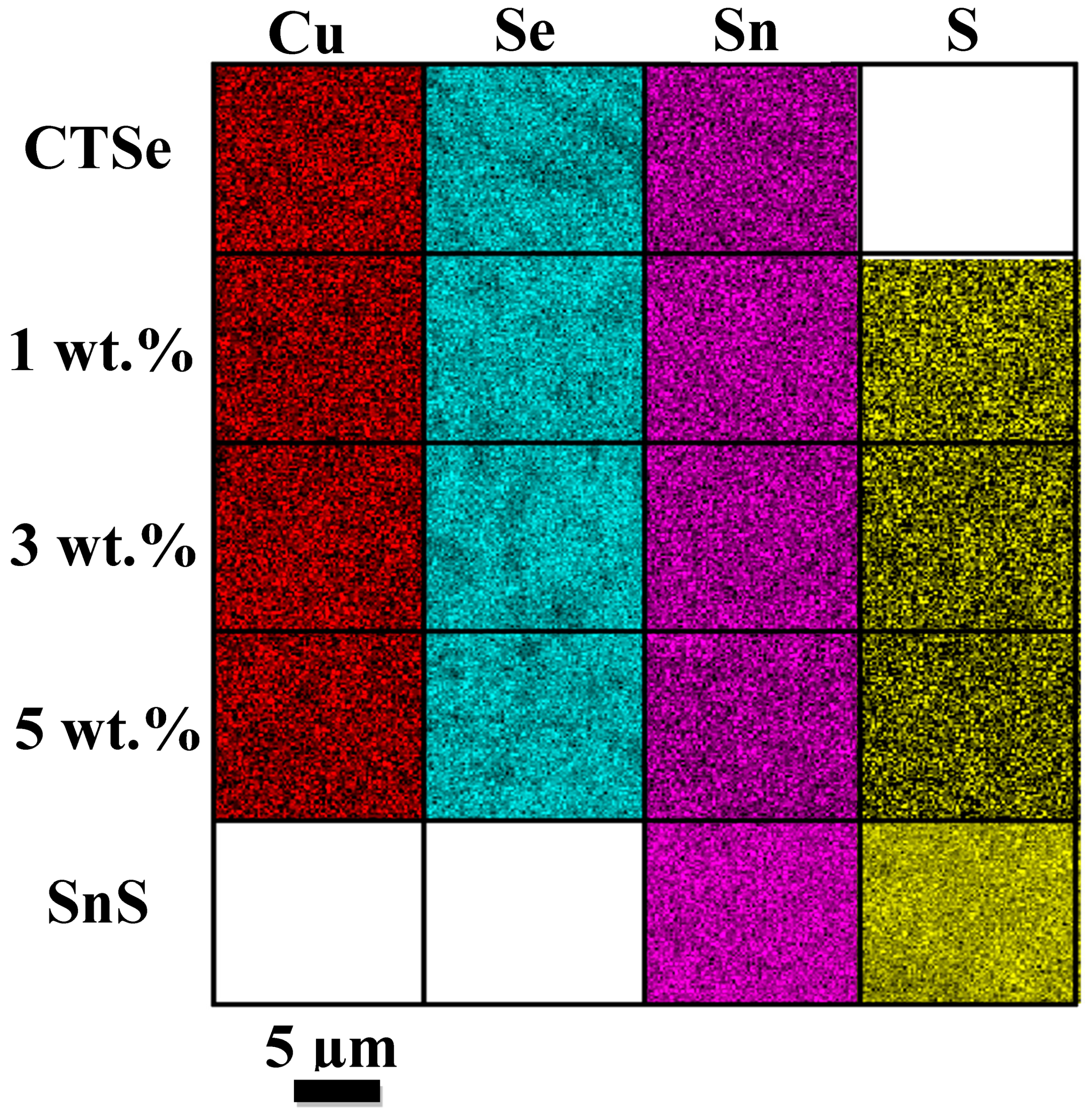
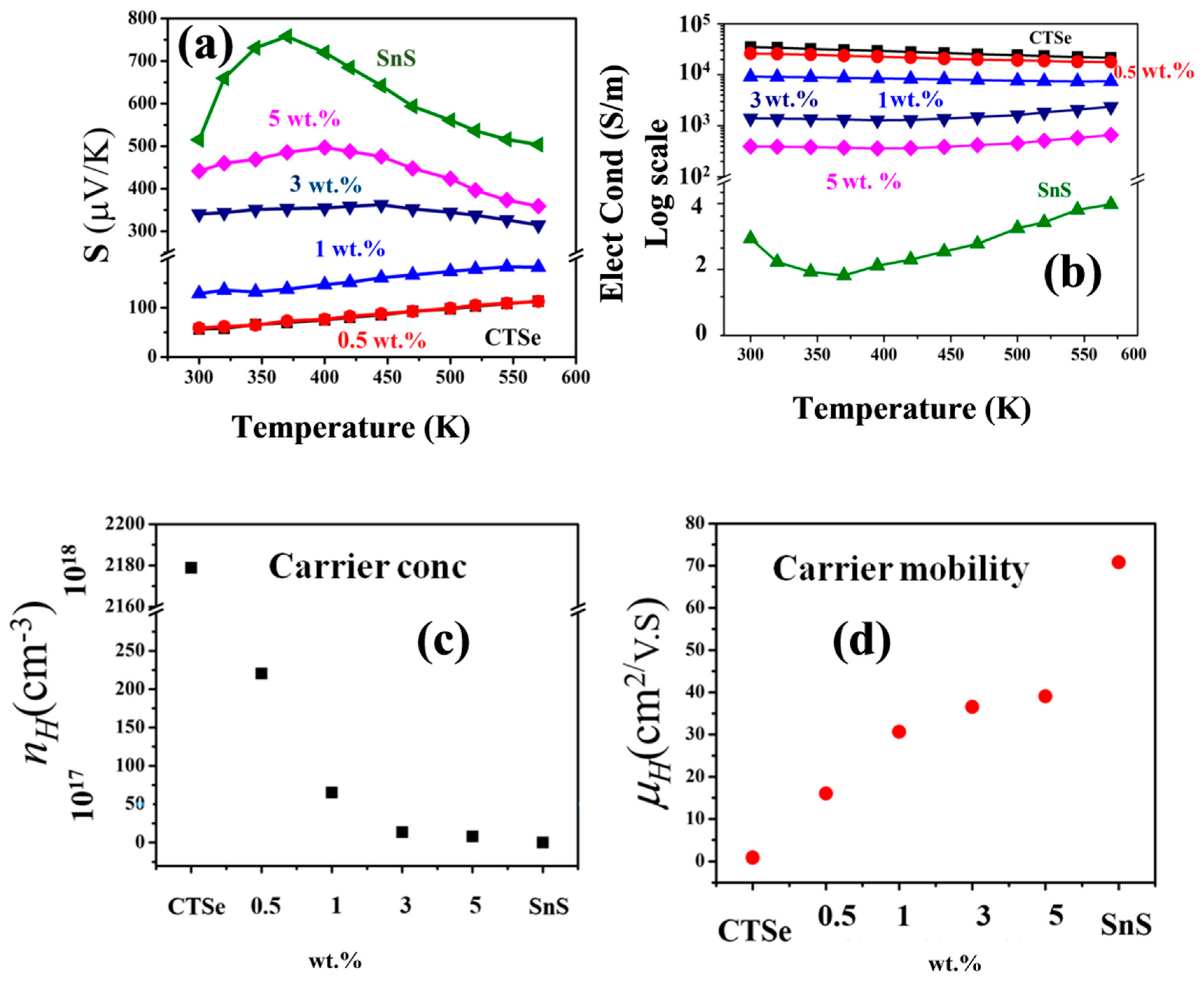
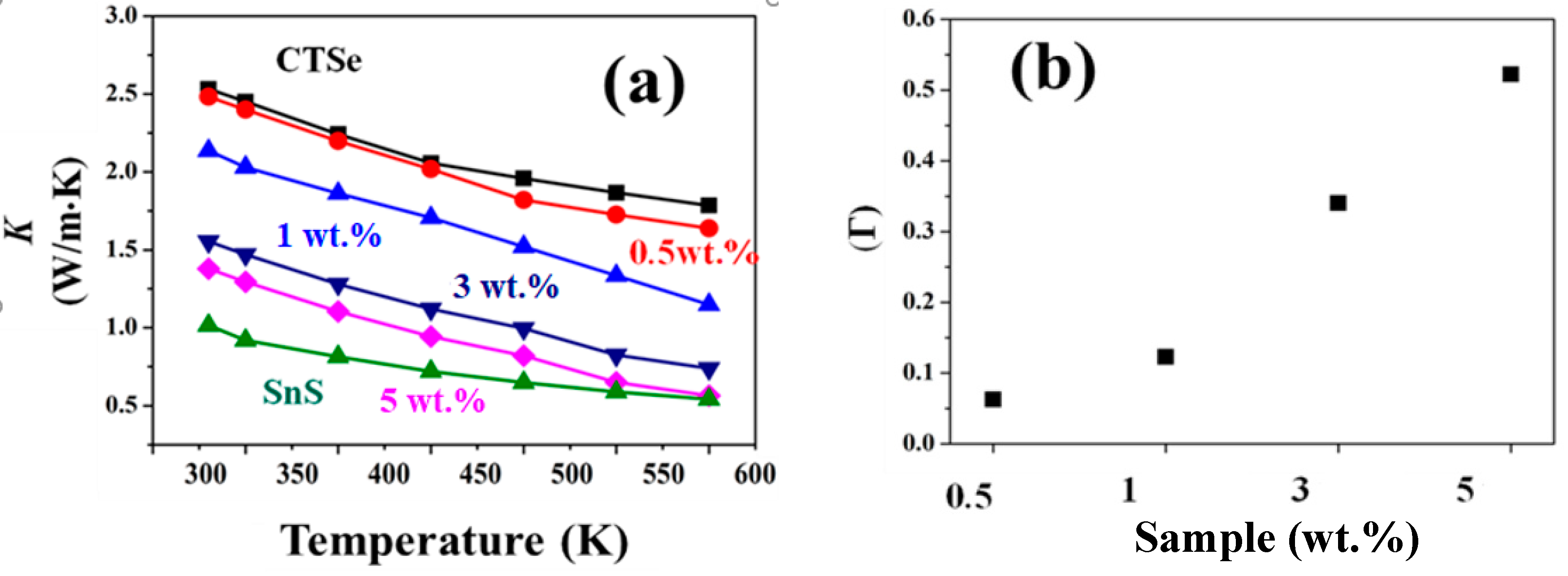
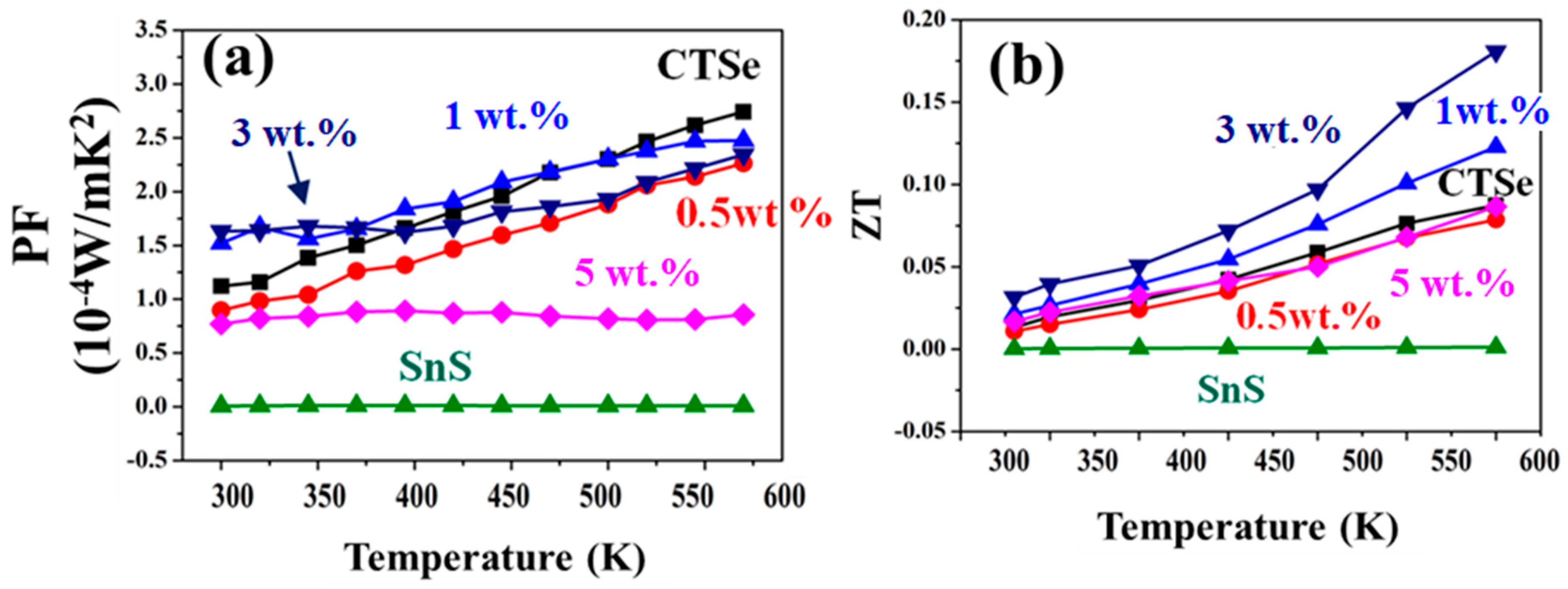
3. Results and Discussion
4. Conclusions
Author Contributions
Funding
Acknowledgments
Conflicts of Interest
References
- Bell, L.E. Cooling, Heating, Generating Power, and Recovering Waste Heat with Thermoelectric Systems. Science 2008, 321, 1457–1461. [Google Scholar] [CrossRef] [PubMed] [Green Version]
- Minnich, A.; Dresselhaus, M.S.; Ren, Z.F.; Chen, G. Bulk Nanostructured Thermoelectric Materials: Current Research and Future Prospects. Energy Environ. Sci. 2009, 2, 466–479. [Google Scholar] [CrossRef]
- Park, D.; Ju, H.; Oh, T.; Kim, J. Facile Fabrication of One-Dimensional Te/Cu2Te Nanorod Composites with Improved Thermoelectric Power Factor and Low Thermal Conductivity. Sci. Rep. 2018, 8, 18082. [Google Scholar] [CrossRef] [PubMed]
- Biswas, K.; He, J.; Blum, I.D.; Wu, C.I.; Hogan, T.P.; Seidman, D.N.; Dravid, V.P.; Kanatzidis, M.G. High-Performance Bulk Thermoelectrics with All-Scale Hierarchical Architectures. Nature 2012, 489, 414. [Google Scholar] [CrossRef] [PubMed]
- Mehta, R.J.; Zhang, Y.; Karthik, C.; Singh, B.; Siegel, R.W.; Borca-Tasciuc, T.; Ramanath, G. A New Class of Doped Nanobulk High-Figure-of-Merit Thermoelectrics by Scalable Bottom-up Assembly. Nat. Mater. 2012, 11, 233–240. [Google Scholar] [CrossRef] [PubMed]
- Zhao, L.; Fei, F.Y.; Wang, J.; Wang, F.; Wang, C.; Li, J.; Wang, Y.; Cheng, Z.; Dou, S.; Wang, X. Improvement of Thermoelectric Properties and Their Correlations with Electron Effective Mass in Cu1.98SxSe1−X. Sci. Rep. 2017, 7, 40436. [Google Scholar] [CrossRef]
- Chauhan, N.S.; Bhardwaj, A.; Senguttuvan, T.D.; Pant, R.P.; Mallikd, R.C.; Misra, D.K. A Synergistic Combination of Atomic Scale Structural Engineering and Panoscopic Approach in P-Type Zrcosb-Based Half-Heusler Thermoelectric Materials for Achieving High Zt. J. Mater. Chem. C 2016, 4, 5766–5778. [Google Scholar] [CrossRef]
- Zhang, C.H.; Ng, H.; Li, Z.; Khor, K.A.; Xiong, Q.H. Minority Carrier Blocking to Enhance the Thermoelectric Performance of Solution-Processed BixSb2-XTe3 Nanocomposites Via a Liquid-Phase Sintering Process. ACS Appl. Mater. Interfaces 2017, 9, 12501–12510. [Google Scholar] [CrossRef]
- Song, D.X.; Ma, W.G.; Zhang, X. Lattice Thermal Conductivity of Si/Ge Composite Thermoelectric Material: Effect of Si Particle Distribution. Int. J. Energy Res. 2019, 43, 379–390. [Google Scholar] [CrossRef]
- Pei, Y.Z.; LaLonde, A.D.; Heinz, N.A.; Snyder, G.J. High Thermoelectric Figure of Merit in PbTe Alloys Demonstrated in PbTe-CdTe. Adv. Energy Mater. 2012, 2, 670–675. [Google Scholar] [CrossRef]
- Pei, Y.Z.; Gibbs, Z.M.; Gloskovskii, A.; Balke, B.; Zeier, W.G.; Snyder, G.J. Optimum Carrier Concentration in N-Type PbTe Thermoelectrics. Adv. Energy Mater. 2014, 4, 1400486. [Google Scholar] [CrossRef]
- Byeon, D.; Sobota, R.; Delime-Codrin, K.; Choi, S.; Hirata, K.; Adachi, M.; Kiyama, M.; Matsuura, T.; Yamamoto, Y.; Matsunami, M.; et al. Discovery of Colossal Seebeck Effect in Metallic Cu2Se. Nat. Commun. 2019, 10. [Google Scholar] [CrossRef] [PubMed]
- Liu, Y.; Zhao, L.D.; Liu, Y.C.; Lan, J.L.; Xu, W.; Li, F.; Zhang, B.P.; Berardan, D.; Dragoe, N.; Lin, Y.H.; et al. Remarkable Enhancement in Thermoelectric Performance of BiCuSeO by Cu Deficiencies. J. Am. Chem. Soc. 2011, 133, 20112–20115. [Google Scholar] [CrossRef] [PubMed]
- Williamson, G.K.; Hall, W.H. X-ray line broadening from filed aluminium and wolfram. Acta Metall. 1953, 1, 122–131. [Google Scholar] [CrossRef]
- Aly, K.A.; Khalil, N.M.; Algamal, Y.; Saleem, Q.M.A. Estimation of Lattice Strain for Zirconia Nano-Particles Based on Williamson-Hall Analysis. Mater. Chem. Phys. 2017, 193, 182–188. [Google Scholar] [CrossRef]
- Banik, A.; Vishal, B.; Perumal, S.; Datta, R.; Biswas, K. The Origin of Low Thermal Conductivity in Sn1−XSbxTe: Phonon Scattering Via Layered Intergrowth Nanostructures. Energy Environ. Sci. 2016, 9, 2011–2019. [Google Scholar] [CrossRef]
- Hobbs, C.C.; Fonseca, L.R.C.; Knizhnik, A.; Dhandapani, V.; Samavedam, S.B.; Taylor, W.J.; Grant, J.M.; Dip, L.G.; Triyoso, D.H.; Hegde, R.I.; et al. Fermi-Level Pinning at the Polysilicon/Metal Oxide Interface—Part I. IEEE Trans. Electron Dev. 2004, 51, 971–977. [Google Scholar] [CrossRef]
- Wang, C.; Chen, Y.D.; Jiang, J.; Zhang, R.; Niu, Y.; Zhou, T.; Xia, J.F.; Tian, H.Q.; Hu, J.; Yang, P. Improved Thermoelectric Properties of SnS Synthesized by Chemical Precipitation. RSC Adv. 2017, 7, 16795–16800. [Google Scholar] [CrossRef]
- Abeles, B. Lattice Thermal Conductivity of Disordered Semiconductor Alloys at High Temperatures. Phys. Rev. 1963, 131, 1906. [Google Scholar] [CrossRef]
- Alekseeva, G.T.; Efimova, B.A.; Ostrovskaya, L.M.; Serebryannikova, O.S.; Tsypin, M.I. Thermal conductivity of solid solutions based on lead telluride. Sov. Phys. Semicond. 1971, 4, 1122–1125. [Google Scholar]
- Wang, H.; LaLonde, A.D.; Pei, Y.Z.; Snyder, G.J. The Criteria for Beneficial Disorder in Thermoelectric Solid Solutions. Adv. Funct. Mater. 2013, 23, 1586–1596. [Google Scholar] [CrossRef]
- Wang, H.; Wang, J.L.; Cao, X.L.; Snyder, G.J. Thermoelectric Alloys between PbSe and PbS with Effective Thermal Conductivity Reduction and High Figure of Merit. J. Mater. Chem. A 2014, 2, 3169–3174. [Google Scholar] [CrossRef]
- Jin, H.Y.; Jaworski, C.M.; Heremans, J.P. Enhancement in the Figure of Merit of P-Type Bi100–XSbx Alloys through Multiple Valence-Band Doping. Appl. Phys. Lett. 2012, 101. [Google Scholar] [CrossRef]
- Anderson, O.L.; Nafe, J.E. The Bulk Modulus-Volume Relationship for Oxide Compounds and Related Geophysical Problems. J. Geophys. Res. 1965, 70, 3951–3963. [Google Scholar] [CrossRef]
- Anderson, D.L.; Anderson, O.L. The Bulk Modulus Volume Relationship for Oxides. J. Geophys. Res. 1970, 75, 3494–3500. [Google Scholar] [CrossRef]
- Callaway, J.; von Baeyer, H.C. Effect of Point Imperfections on Lattice Thermal Conductivity. Phys. Rev. 1960, 120, 1149. [Google Scholar] [CrossRef]
- Klemens, P.G. Thermal Resistance Due to Point Defects at High Temperatures. Phys. Rev. 1960, 119, 507. [Google Scholar] [CrossRef]
- Qiu, P.F.; Huang, X.Y.; Chen, X.H.; Chen, L.D. Enhanced Thermoelectric Performance by the Combination of Alloying and Doping in TiCoSb-Based Half-Heusler Compounds. J. Appl. Phys. 2009, 106, 103703. [Google Scholar] [CrossRef]
- Pei, Y.Z.; Wang, H.; Snyder, G.J. Band Engineering of Thermoelectric Materials. Adv. Mater. 2012, 24, 6125–6135. [Google Scholar] [CrossRef] [PubMed]
- Fan, J.; Schnelle, W.; Antonyshyn, I.; Veremchuk, I.; Carrillo-Cabrera, W.; Shi, X.; Grin, Y.; Chen, L.D. Structural Evolvement and Thermoelectric Properties of Cu3−XSnxSe3 Compounds with Diamond-Like Crystal Structures. Dalton Trans. 2014, 43, 16788–16794. [Google Scholar] [CrossRef] [PubMed]
- Li, Y.Y.; Liu, G.H.; Cao, T.F.; Liu, L.M.; Li, J.T.; Chen, K.X.; Li, L.F.; Han, Y.M.; Zhou, M. Enhanced Thermoelectric Properties of Cu2SnSe3 by (Ag, In)-Co-Doping. Adv. Funct. Mater. 2016, 26, 6025–6032. [Google Scholar] [CrossRef]
- Shi, X.Y.; Xi, L.L.; Fan, J.; Zhang, W.Q.; Chen, L.D. Cu-Se Bond Network and Thermoelectric Compounds with Complex Diamondlike Structure. Chem. Mater. 2010, 22, 6029–6031. [Google Scholar] [CrossRef]


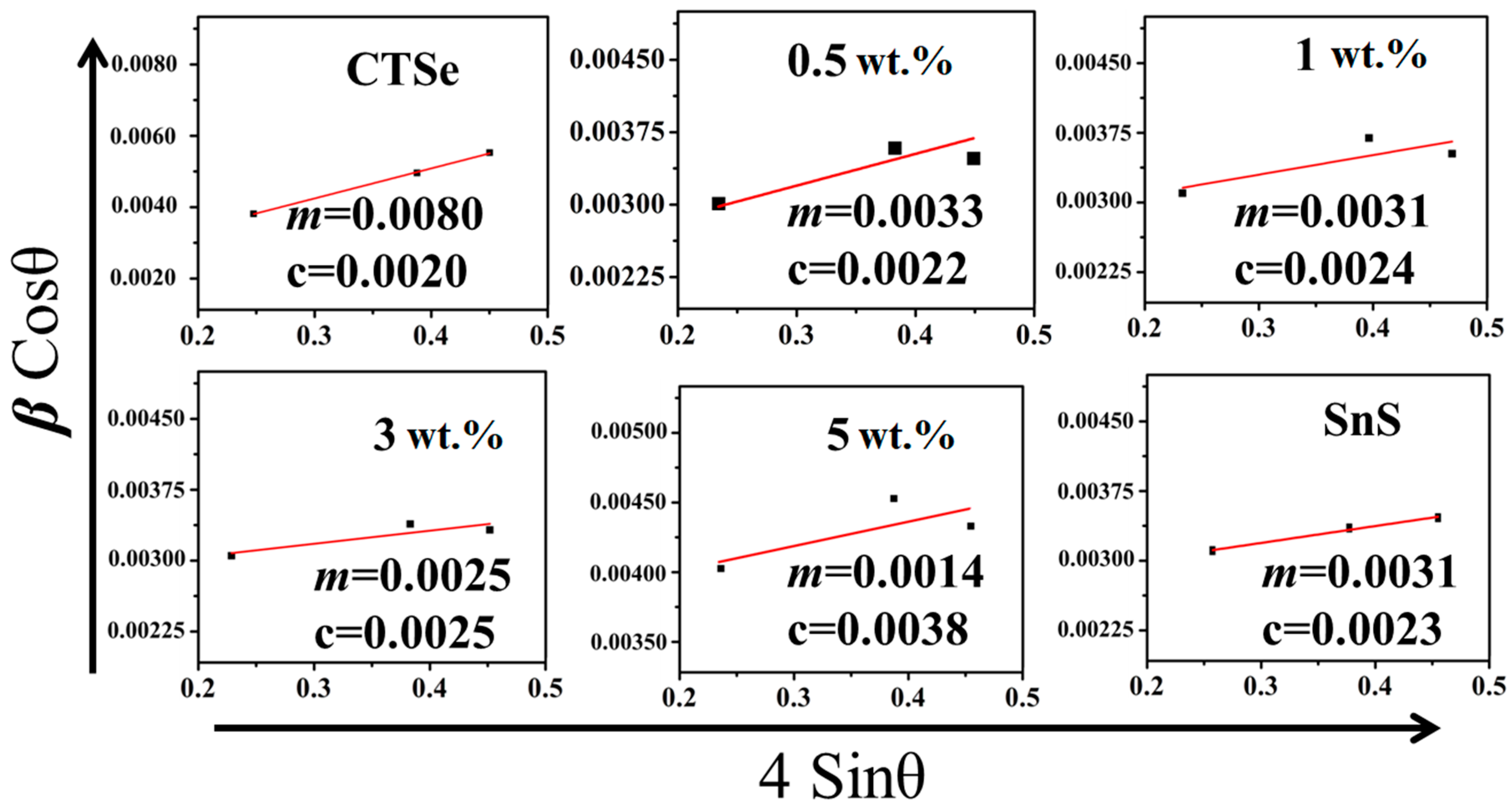
| Sample | Scherer’s Method | W-H Method | |
|---|---|---|---|
| UDM | |||
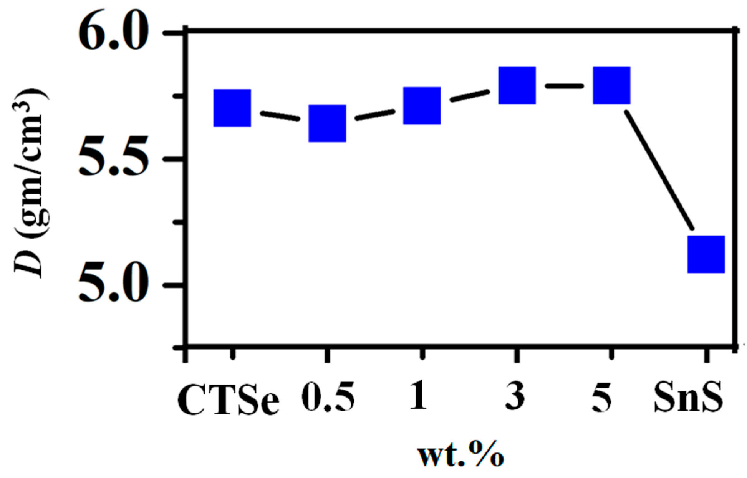
| D (nm) | D (nm) | ε (10−3) | |
| CTSe | 49.21 | 67.97 | 8.03 |
| 0.5 wt.% | 41.39 | 62.74 | 3.29 |
| 1 wt.% | 40.47 | 58.50 | 3.07 |
| 3 wt.% | 38.42 | 55.91 | 2.47 |
| 5 wt.% | 32.14 | 36.30 | 1.41 |
| SnS | 34.62 | 60.02 | 3.46 |
| Sample | Carrier Conc | Carrier Mobility |
|---|---|---|
| nH (cm−3) (1017) | μH (cm2/V·S) | |
| CTSe | 21788.21 | 0.89 |
| 0.5 wt.% | 220.35 | 16.03 |
| 1 wt.% | 65.15 | 30.67 |
| 3 wt.% | 13.58 | 36.56 |
| 5 wt.% | 0.80 | 39.05 |
| SnS | 0.02 | 73.23 |
© 2019 by the authors. Licensee MDPI, Basel, Switzerland. This article is an open access article distributed under the terms and conditions of the Creative Commons Attribution (CC BY) license (http://creativecommons.org/licenses/by/4.0/).
Share and Cite
Siyar, M.; Cho, J.-Y.; Jin, W.-C.; Hwang, E.H.; Kim, M.; Park, C. Thermoelectric Properties of Cu2SnSe3-SnS Composite. Materials 2019, 12, 2040. https://doi.org/10.3390/ma12132040
Siyar M, Cho J-Y, Jin W-C, Hwang EH, Kim M, Park C. Thermoelectric Properties of Cu2SnSe3-SnS Composite. Materials. 2019; 12(13):2040. https://doi.org/10.3390/ma12132040
Chicago/Turabian StyleSiyar, Muhammad, Jun-Young Cho, Woo-Chan Jin, Euy Heon Hwang, Miyoung Kim, and Chan Park. 2019. "Thermoelectric Properties of Cu2SnSe3-SnS Composite" Materials 12, no. 13: 2040. https://doi.org/10.3390/ma12132040