Improvement on Fully Filled Through Silicon Vias by Optimized Sputtering and Electroplating Conditions

Abstract
:1. Introduction
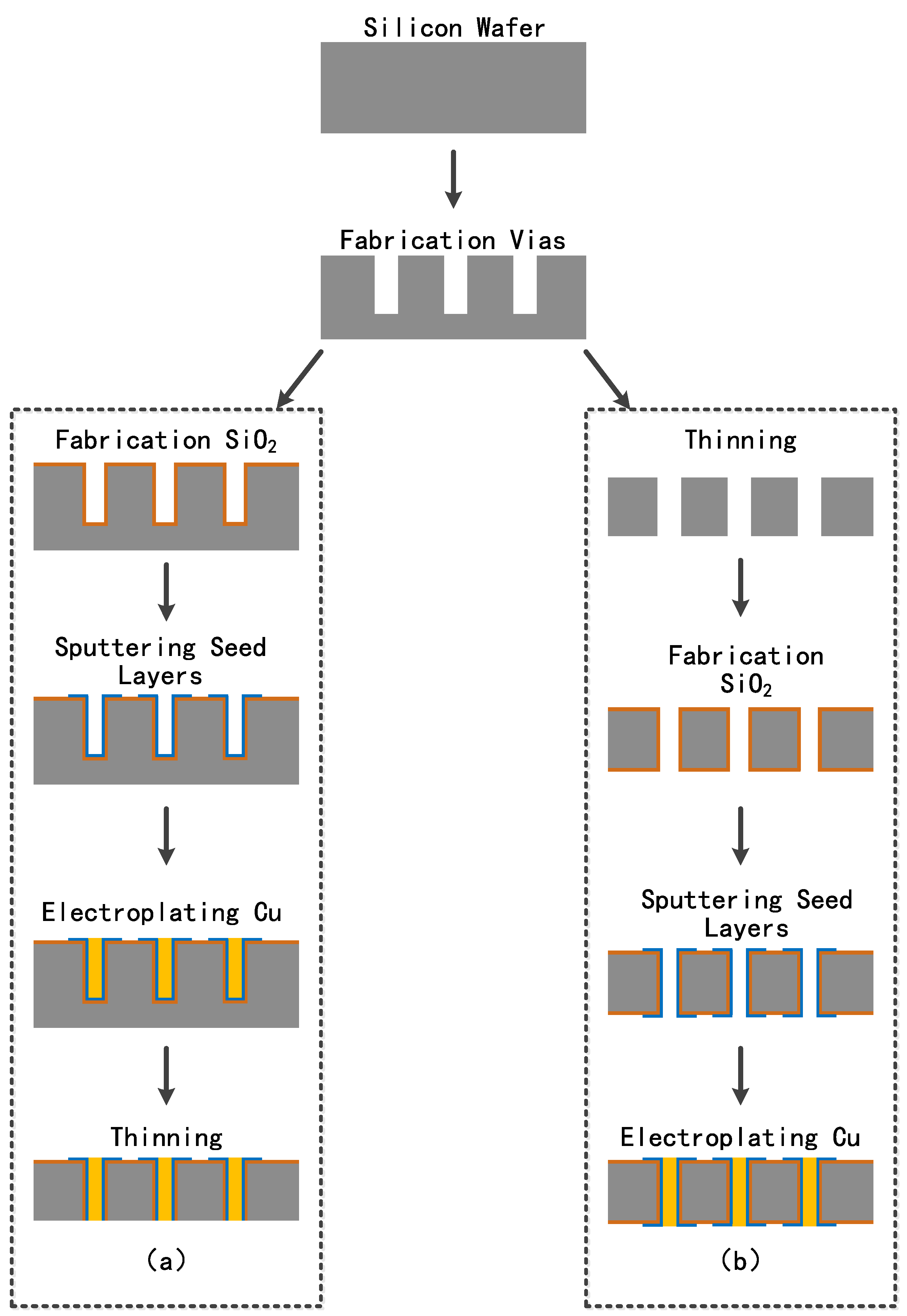
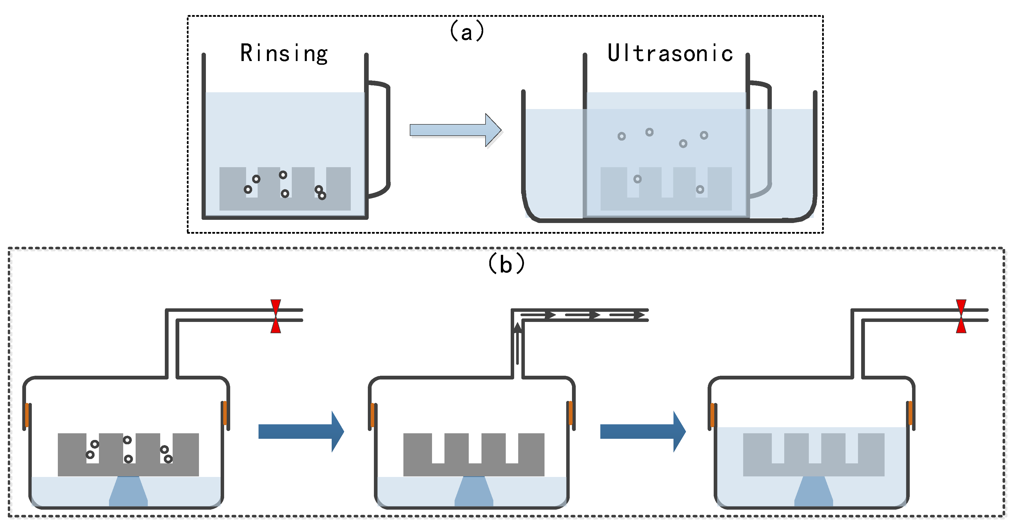
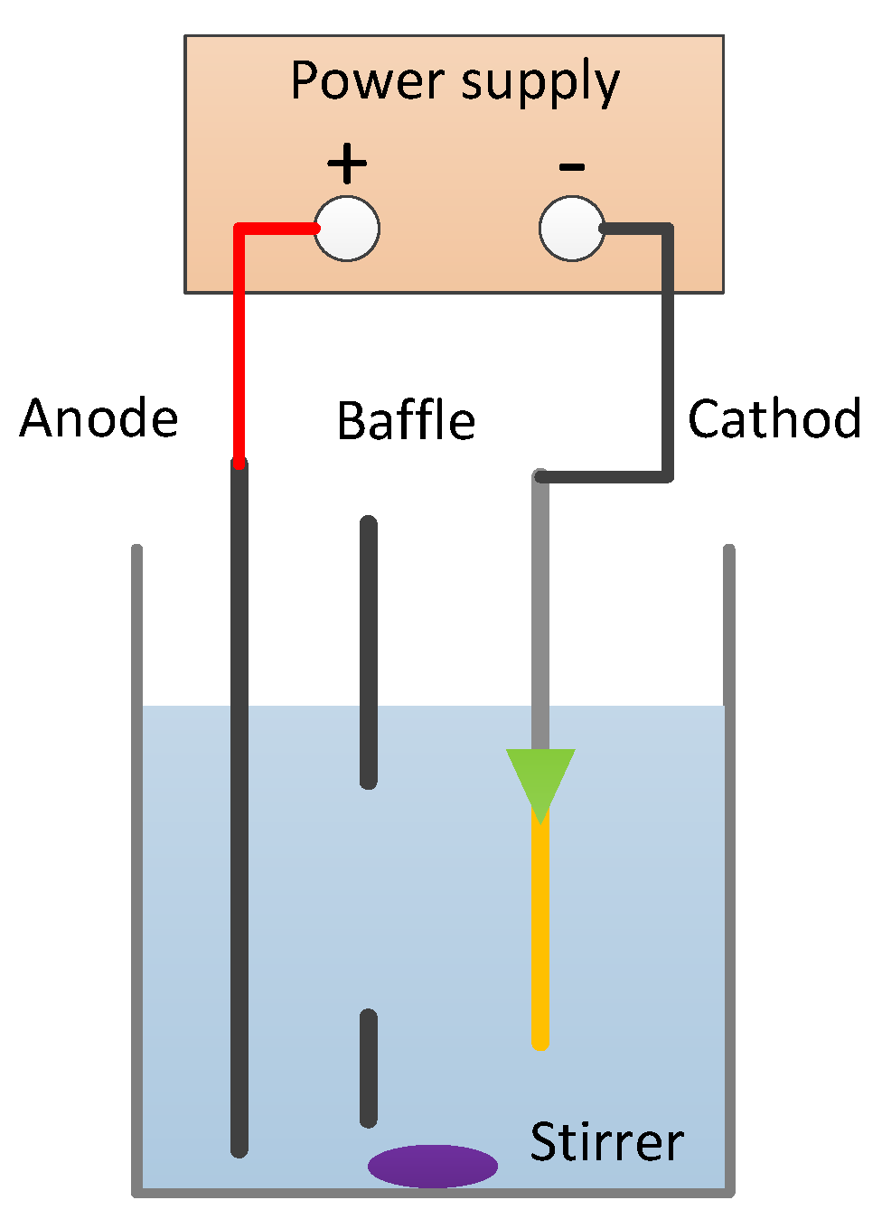
2. Materials and Methods
3. Results and Discussions
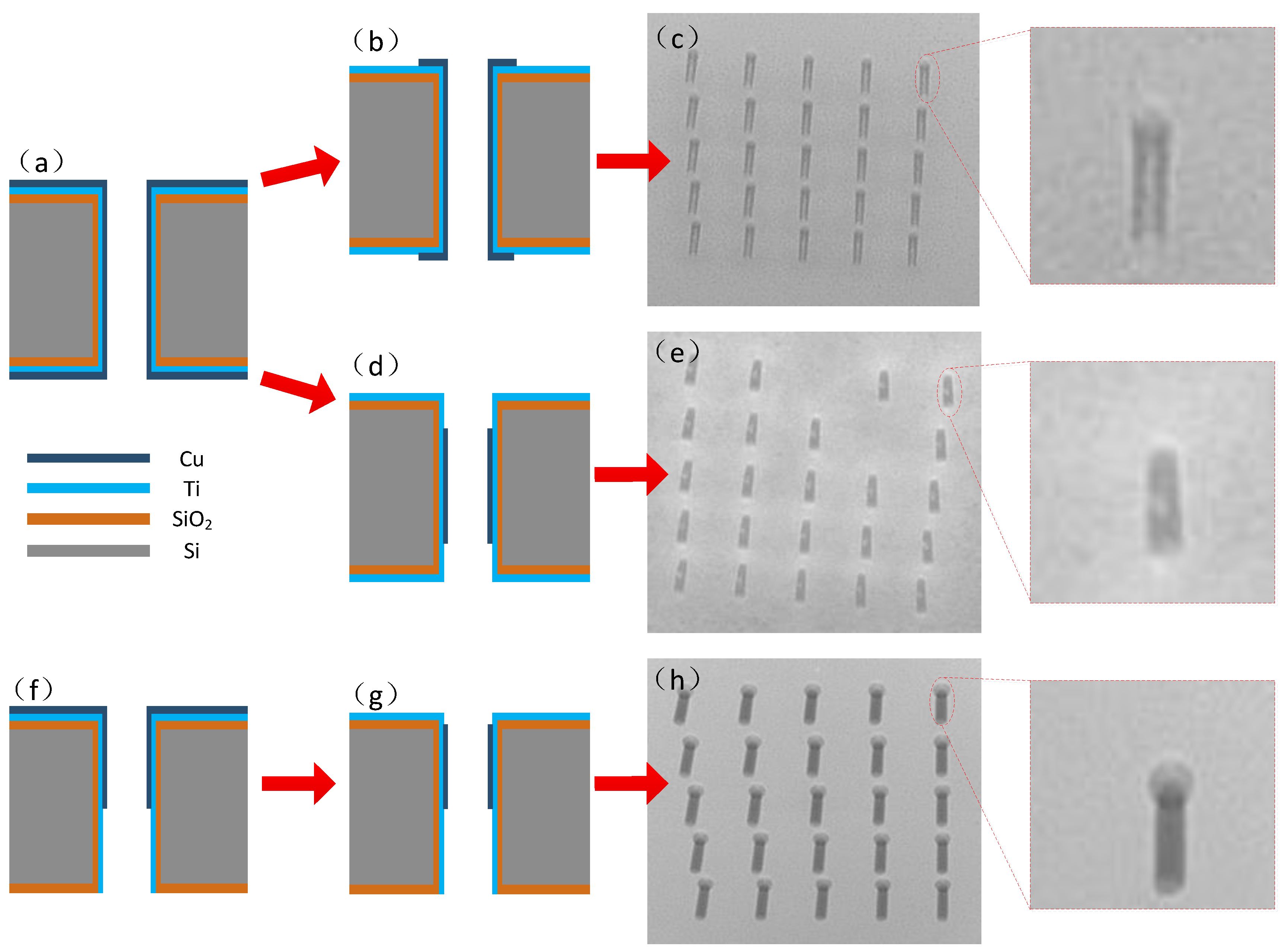
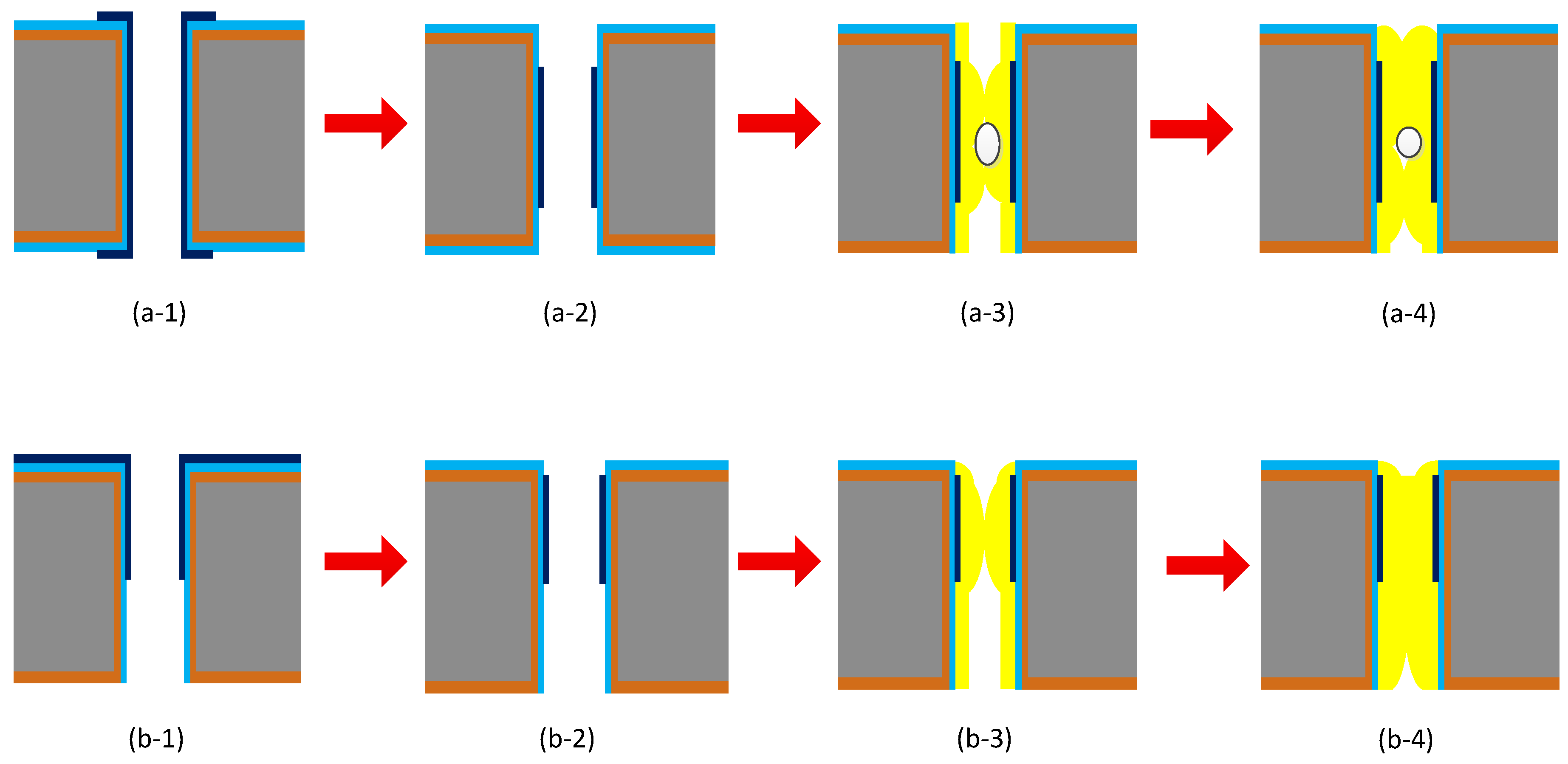
3.1. Improvement of Sputtering
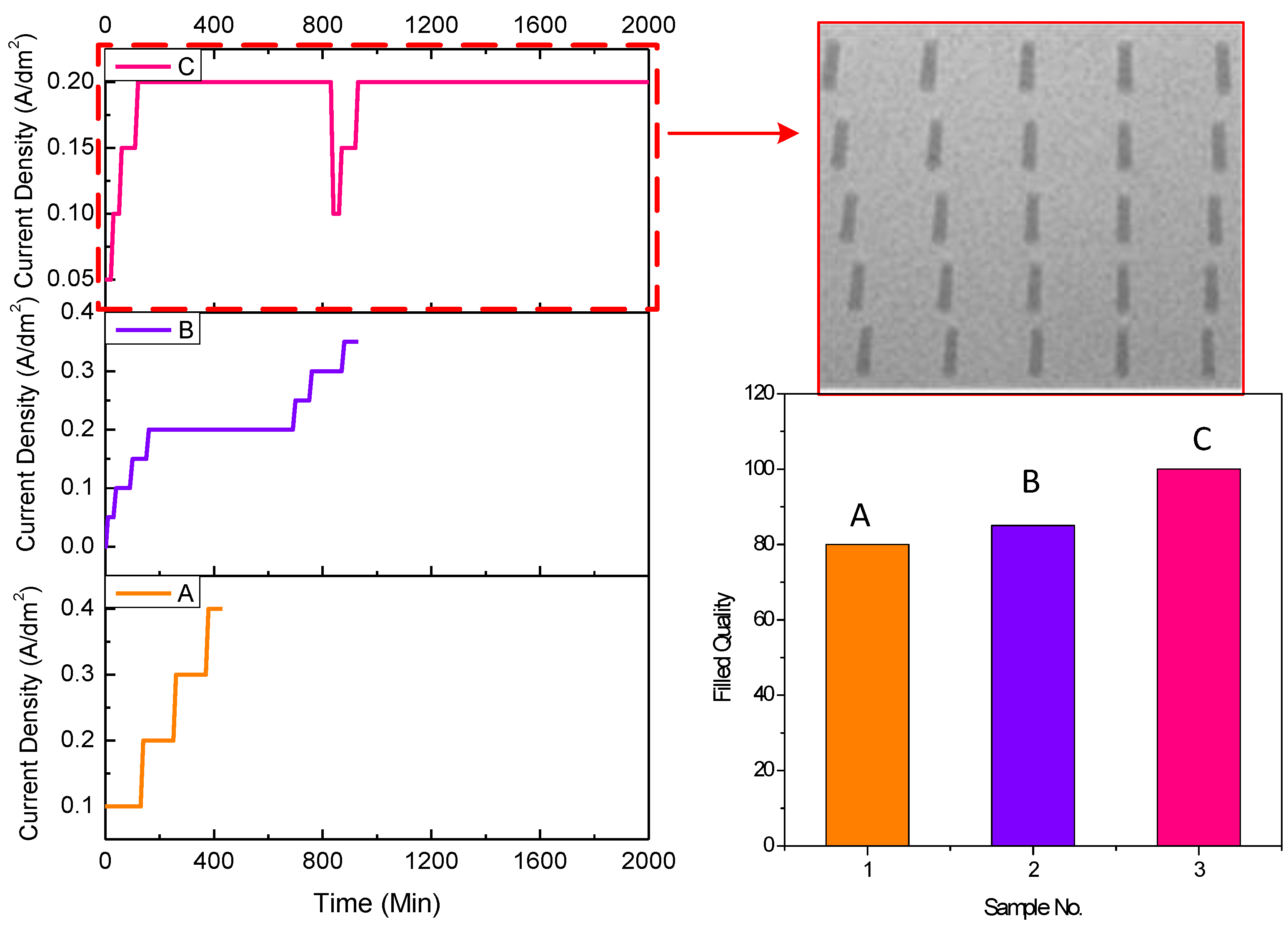
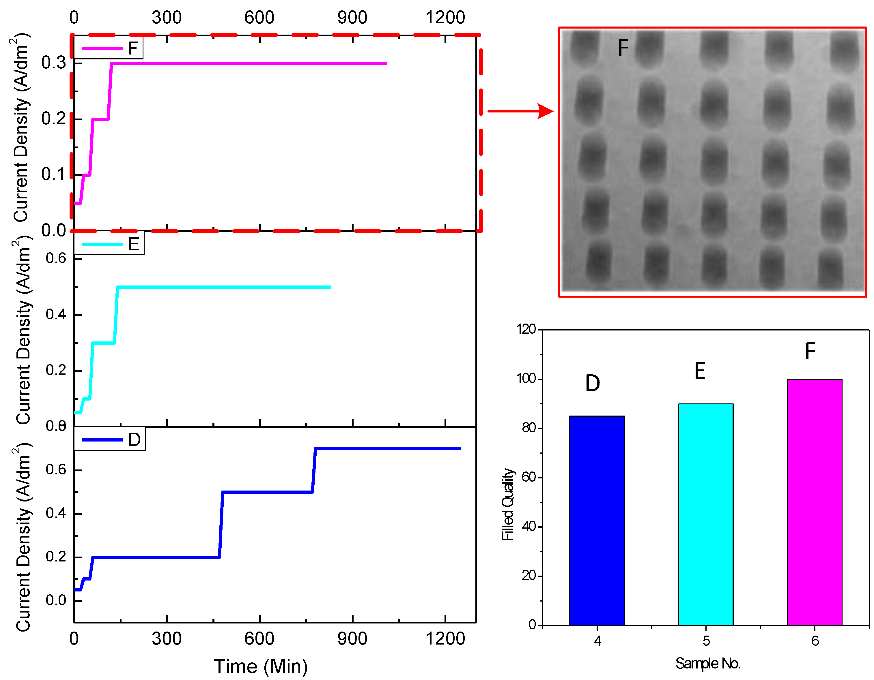
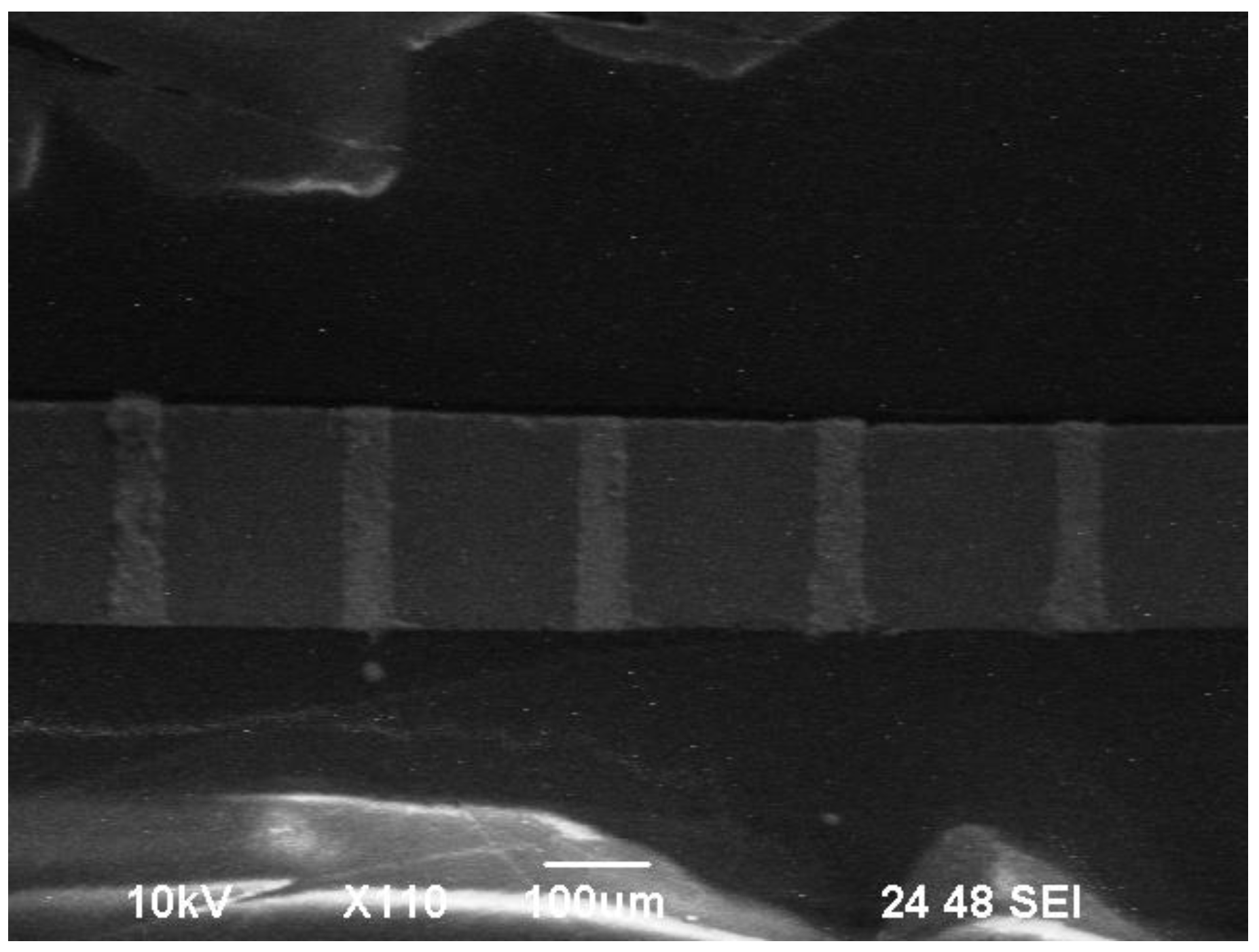
3.2. Improvement of Electroplating Condition
4. Conclusions
Funding
Conflicts of Interest
References
- Knickerbocker, J.U.; Patel, C.S.; Andry, P.S.; Tsang, C.K.; Buchwalter, L.P.; Sprogis, E.J.; Gan, H.; Horton, R.R.; Polastre, R.J.; Wright, S.L.; et al. 3-D Silicon integration and silicon packaging technology using silicon through-vias. IEEE J. Solid State Circuits 2006, 41, 1718–1725. [Google Scholar] [CrossRef]
- Ho, S.W.; Yoon, S.W.; Zhou, Q.; Pasad, K.; Kripesh, V.; Lau, J.H. High RF performance TSV silicon carrier for high frequency application. In Proceedings of the Electronic Components and Technology Conference (ECTC), Lake Buena Vista, FL, USA, 27–30 May 2008; pp. 1946–1952. [Google Scholar]
- Ngansso, S.; Fischer, P. TSV Through silicon via technology for 3D-integration. In Proceedings of the 2010 IEEE International Memory Workshop, Seoul, Korea, 16–19 May 2010. [Google Scholar]
- Zhang, Y.; Ding, G.; Hong, W.; Cheng, P.; Liu, R. Optimization of innovative approaches to the shortening of filling times in 3D integrated through-silicon vias (TSVs). J. Micromech. Microeng. 2015, 25, 045009. [Google Scholar] [CrossRef]
- Pohjoranta, A.; Tenno, R. A method for microvia-fill process modeling in a Cu plating system with additives. J. Electrochem. Soc. 2007, 154, D502–D509. [Google Scholar] [CrossRef]
- Olmen, J.V.; Huyghebaert, C.; Coenen, J.; Aelst, J.V.; Sleeckx, E.; Ammel, A.V.; Armini, S.; Katti, G.; Vaes, J.; Dehaene, W.; et al. Integration challenges of copper through silicon via (TSV) metallization for 3D-stacked IC integration. Microelectron. Eng. 2011, 88, 745–748. [Google Scholar] [CrossRef]
- Wolf, M.J.; Dretschkow, T.; Wunderle, B.; Jurgensen, N.; Engelmann, G.; Ehrmann, O.; Uhlig, A.; Michel, B.; Reichl, H. High aspect ratio TSV copper filling with different seed layers. In Proceedings of the Electronic Components and Technology Conference (ECTC), Lake Buena Vista, FL, USA, 27–30 May 2008; pp. 563–570. [Google Scholar]
- Li, H.Y.; Liao, E.; Pang, X.F.; Yu, H.; Yu, X.X.; Sun, J.Y. Fast electroplating TSV process development for the via-last approach. In Proceedings of the Electronic Components and Technology Conference (ECTC), Las Vegas, NV, USA, 1–4 June 2010; pp. 777–780. [Google Scholar]
- Li, Y.; Cao, H.; Feng, X.; Ling, H.; Li, M.; Sun, J. Effect of different pretreatment on through silicon via copper filling. In Proceedings of the International Conference on Electronic Packaging Technology, Dalian, China, 11–14 August 2013; pp. 169–172. [Google Scholar]
- Lu, Y.; Cao, H.; Sun, Q.; Ling, H.; Li, M.; Sun, J. Investigation of competitive adsorption between accelerator and suppressor in TSV copper electroplating. In Proceedings of the International Conference on Electronic Packaging Technology & High Density Packaging (ICEPT-HDP), Guilin, China, 13–16 August 2012; pp. 434–437. [Google Scholar]
- Tian, Q.; Cai, J.; Zheng, J.; Zhou, C.; Li, J.; Zhu, W. Copper pulse-reverse current electrodeposition to fill blind vias for 3-D TSV integration. IEEE Trans. Compon. Packag. Manuf. Technol. 2017, 6, 1899–1904. [Google Scholar] [CrossRef]
- Wu, C.; Wei, C.; Li, Y. In situ mechanical characterization of the mixed-mode fracture strength of the Cu/Si interface for TSV structures. Miecronachines 2019, 10, 86. [Google Scholar] [CrossRef] [PubMed]
- Shin, S.H.; Kim, T.Y.; Park, J.H.; Suh, S.J. Optimization of additive and current conditions for void-free filled through-silicon via. Appl. Sci. 2018, 8, 2135. [Google Scholar] [CrossRef]
- Sun, F.L.; Liu, Z.Q.; Li, C.F.; Zhu, Q.S.; Zhang, H.; Suganuma, K. Bottom–up electrodeposition of large-scale nanotwinned copper within 3D through silicon via. Materials 2018, 11, 319. [Google Scholar] [CrossRef] [PubMed]
- Song, C.; Xue, K.; Yang, S.; Yong, Z.; Li, H.; Xue, H.; Jing, X.; Lee, U. Silicon interposer process development for advanced system integration. Microelectron. Eng. 2016, 156, 50–54. [Google Scholar]
- Zhang, Y.; Wang, H.; Sun, Y.; Wu, K.; Wang, H.; Cheng, P.; Ding, G. Copper electroplating technique for efficient manufacturing of low-cost silicon interposers. Microelectron. Eng. 2016, 150, 39–42. [Google Scholar] [CrossRef]
- Kia, A.M.; Haufe, N.; Esmaeili, S.; Mart, C.; Utriainen, M.; Puurunen, R.L.; Weinreich, W. ToF-SIMS 3D analysis of thin films deposited in high aspect ratio structures via atomic layer deposition and chemical vapor deposition. Nanomaterials 2019, 9, 1035. [Google Scholar] [CrossRef] [PubMed]
- Meng, M.; Cheng, L.; Yang, K.; Sun, M.; Luo, Y. A novel seedless TSV process based on room temperature curing silver nanowires ECAs for MEMS packaging. Micromachines 2019, 10, 351. [Google Scholar] [CrossRef] [PubMed]
- Li, H.; Liu, J.; Xu, T.; Xia, J.; Tan, X.; Tao, Z. Fabrication and optimization of high aspect ratio through-silicon-vias electroplating for 3D inductor. Micromachines 2018, 9, 528. [Google Scholar] [CrossRef] [PubMed]
- Chiu, Y.D.; Dow, W.P. Accelerator screening by cyclic voltammetry for microvia filling by copper electroplating. J. Electrochem. Soc. 2013, 160, D3021–D3027. [Google Scholar] [CrossRef]
- Tu, H.; Yen, P.; Chen, S.; Yau, S.; Dow, W.; Lee, Y. In situ STM imaging of Bis-3-sodiumsulfopropyl-disulfide molecules adsorbed on copper film electrodeposited on Pt(1 1 1) single crystal electrode. Langmuir 2011, 27, 6801. [Google Scholar] [CrossRef] [PubMed]


© 2019 by the author. Licensee MDPI, Basel, Switzerland. This article is an open access article distributed under the terms and conditions of the Creative Commons Attribution (CC BY) license (http://creativecommons.org/licenses/by/4.0/).
Share and Cite
Zhao, F. Improvement on Fully Filled Through Silicon Vias by Optimized Sputtering and Electroplating Conditions. Materials 2019, 12, 3713. https://doi.org/10.3390/ma12223713
Zhao F. Improvement on Fully Filled Through Silicon Vias by Optimized Sputtering and Electroplating Conditions. Materials. 2019; 12(22):3713. https://doi.org/10.3390/ma12223713
Chicago/Turabian StyleZhao, Fei. 2019. "Improvement on Fully Filled Through Silicon Vias by Optimized Sputtering and Electroplating Conditions" Materials 12, no. 22: 3713. https://doi.org/10.3390/ma12223713
APA StyleZhao, F. (2019). Improvement on Fully Filled Through Silicon Vias by Optimized Sputtering and Electroplating Conditions. Materials, 12(22), 3713. https://doi.org/10.3390/ma12223713