Facile Process for Surface Passivation Using (NH4)2S for the InP MOS Capacitor with ALD Al2O3


Abstract
:1. Introduction
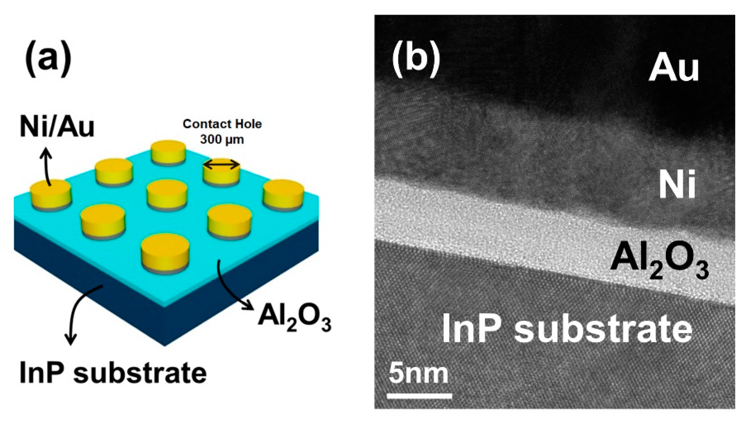
2. Experimental
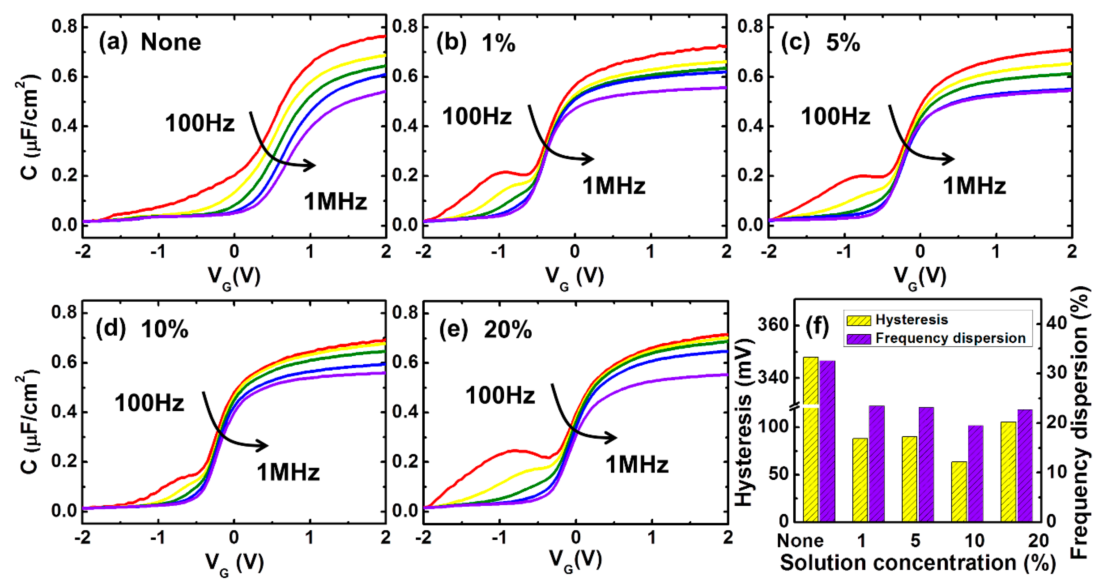
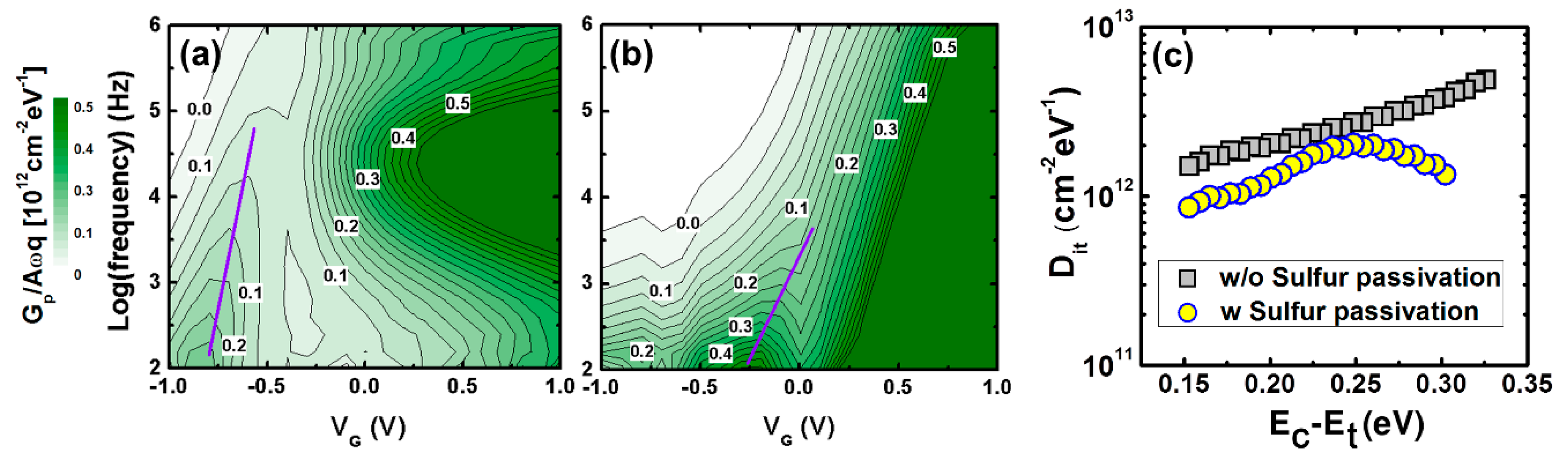
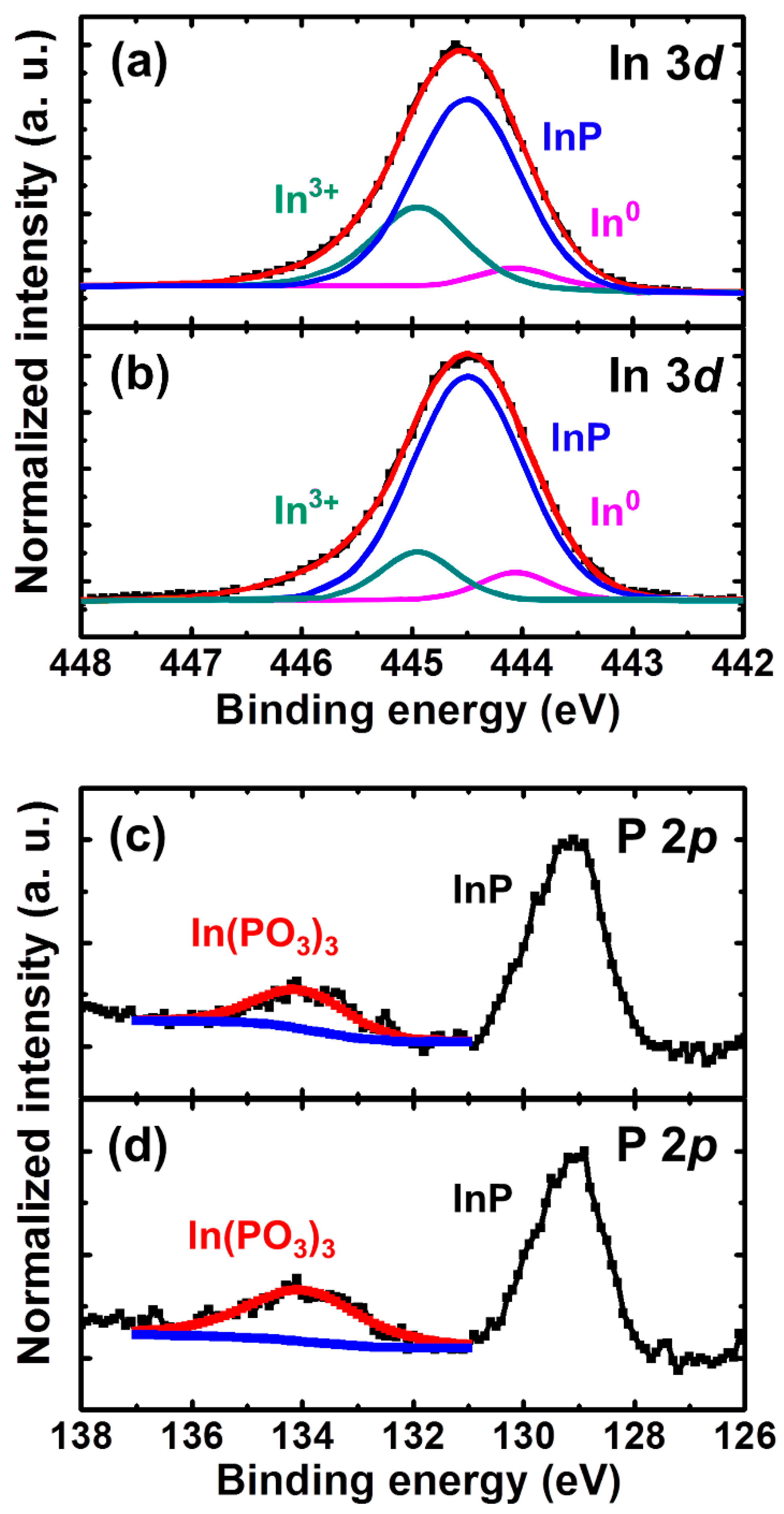
3. Discussion and Results
4. Conclusions
Supplementary Materials
Author Contributions
Funding
Acknowledgments
Conflicts of Interest
References
- Zhao, H.; Shahrjerdi, D.; Zhu, F.; Kim, H.S.; Ok, I.; Zhang, M.; Yum, J.H.; Banerjee, S.K.; Lee, J.C. Inversion-type indium phosphide metal-oxide-semiconductor field-effect transistors with equivalent oxide thickness of 12 Å using stacked HfAlOx/HfO2 gate dielectric. Appl. Phys. Lett. 2008, 92, 203506. [Google Scholar]
- Wu, Y.Q.; Xuan, Y.; Shen, T.; Ye, P.D.; Cheng, Z.; Lochtefeld, A. Enhancement-mode InP n-channel metal-oxide-semiconductor field-effect transistors with atomic-layer-deposited Al2O3 dielectrics. Appl. Phys. Lett. 2007, 91, 022108. [Google Scholar] [CrossRef]
- Chen, Y.-T.; Zhao, H.; Yum, J.H.; Wang, Y.; Lee, J.C. Metal-oxide-semiconductor field-effect-transistors on indium phosphide using HfO2 and silicon passivation layer with equivalent oxide thickness of 18 Å. Appl. Phys. Lett. 2009, 94, 92–95. [Google Scholar] [CrossRef]
- Zhao, H.; Chen, Y.-T.; Yum, J.; Wang, Y.; Zhou, F.; Xue, F.; Lee, J.C. Effects of barrier layers on device performance of high mobility In0.7Ga0.3As metal-oxide-semiconductor field-effect-transistors. Appl. Phys. Lett. 2010, 96, 102101. [Google Scholar] [CrossRef]
- Black, L.E.; Cavalli, A.; Verheijen, M.A.; Haverkort, J.E.M.; Bakkers, E.P.A.M.; Kessels, W.M.M. Effective Surface Passivation of InP Nanowires by Atomic-Layer-Deposited Al2O3 with POx Interlayer. Nano Lett. 2017, 17, 6287. [Google Scholar] [CrossRef] [PubMed]
- Iyer, R.; Chang, R.R.; Lile, D.L. Sulfur as a surface passivation for InP. Appl. Phys. Lett. 1988, 53, 134. [Google Scholar] [CrossRef]
- Klopfenstein, P.; Bastide, G.; Rouzeyre, M. Interface studies and electrical properties of plasma sulfide layers on n-type InP. J. Appl. Phys. 1988, 63, 150. [Google Scholar] [CrossRef]
- Herman, J.S.; Terry, F.L. Hydrogen sulfide plasma passivation of indium phosphide. J. Electron. Mater. 1993, 22, 119. [Google Scholar] [CrossRef]
- Cuypers, D.; van Dorp, D.H.; Tallarida, M.; Brizzi, S.; Rodriguez, L.; Conard, T.; Arnauts, S.; Schmeisser, D.; Adelmann, C.; de Gendt, S. Study of InP Surfaces after Wet Chemical Treatments. ECS Trans. 2013, 58, 297–303. [Google Scholar] [CrossRef]
- Yen, C.-F.; Lee, M.K. Very Low Leakage Current of High Band-Gap Al2O3 Stacked on TiO2/InP Metal–Oxide–Semiconductor Capacitor with Sulfur and Hydrogen Treatments. Jpn. J. Appl. Phys. 2012, 51, 1201. [Google Scholar]
- Gu, J.J.; Neal, A.T.; Ye, P.D. Effects of (NH4)2S passivation on the off-state performance of 3-dimensional InGaAs metal-oxide-semiconductor field-effect transistors. Appl. Phys. Lett. 2011, 99, 152113. [Google Scholar] [CrossRef]
- Galatage, R.V.; Dong, H.; Zhernokletov, D.M.; Brennan, B.; Hinkle, C.L.; Wallace, R.M.; Vogel, E.M. Electrical and chemical characteristics of Al2O3/InP metal-oxide-semiconductor capacitors. Appl. Phys. Lett. 2013, 102, 132903. [Google Scholar] [CrossRef]
- Alian, A.; Brammertz, G.; Degraeve, R.; Cho, M.; Merckling, C.; Lin, D.; Wang, W.-E.; Caymax, M.; Meuris, M.; Meyer, K.D.; et al. Oxide Trapping in the InGaAs–Al2O3 System and the Role of Sulfur in Reducing the Al2O3 Trap Density. IEEE Electron Devices Lett. 2012, 33, 1544–1546. [Google Scholar] [CrossRef]
- Steven, C.; Witczak, J.; Suehle, S.; Gaitan, M. An experimental comparison of measurement techniques to extract Si-SiO2 interface trap density. Solid-State Electron. 1992, 35, 345–355. [Google Scholar]
- Engel-Herbert, R.; Hwang, Y.; Stemmer, S. Comparison of methods to quantify interface trap densities at dielectric/III-V semiconductor interfaces. J. Appl. Phys. 2010, 108, 124101. [Google Scholar] [CrossRef]
- Brammertz, G.; Alian, A.; Lin, H.C.; Meuris, M.; Caymax, M.; Wang, W.-E. A Combined Interface and Border Trap Model for High-Mobility Substrate Metal–Oxide–Semiconductor Devices Applied to In0.53Ga0.47As and InP Capacitors. IEEE Trans. Electron Devices 2011, 58, 3890–3897. [Google Scholar] [CrossRef]
- Lin, D.H.C.; Brammertz, G.; Sioncke, S.; Nyns, L.; Alian, A.; Wang, W.-E.; Heyns, M.; Caymaxand, M.; Hoffmann, T. Electrical Characterization of the MOS (Metal-Oxide-Semiconductor) System: High Mobility Substrates. ECS Trans. 2011, 34, 1065–1070. [Google Scholar]
- Kim, E.J.; Wang, L.; Asbeck, P.M.; Saraswat, K.C.; McIntyre, P.C. Border traps in Al2O3/In0.53Ga0.47As (100) gate stacks and their passivation by hydrogen anneals. Appl. Phys. Lett. 2010, 96, 012906. [Google Scholar] [CrossRef]
- Hinkle, C.L.; Galatage, R.V.; Zhernokletov, D.M.; Dong, H.; Anwar, S.R.M.; Brennan, B.; Vogel, E.M. III-V/High-k Defects: DIGS vs. Border Traps. ECS Trans. 2013, 53, 161–167. [Google Scholar] [CrossRef]
- Zhernokletov, D.M.; Dong, H.; Brennan, B.; Kim, J.; Wallace, R.M. Optimization of the ammonium sulfide (NH4)2S passivation process on InSb(111)A. J. Vac. Sci. Technol. B 2012, 30, 04E103. [Google Scholar] [CrossRef]
- O’Connor, É.; Brennan, B.; Djara, V.; Cherkaoui, K.; Monaghan, S.; Newcomb, S.B.; Contreras, R.; Milojevic, M.; Hughes, G.; Pemble, M.E.; et al. A systematic study of (NH4)2S passivation (22%, 10%, 5%, or 1%) on the interface properties of the Al2O3/In0.53Ga0.47As/InP system for n-type and p-type In0.53Ga0.47As epitaxial layers. J. Appl. Phys. 2011, 109, 024101. [Google Scholar] [CrossRef]
- Hollinger, G.; Bergignat, E.; Joseph, J.; Robach, Y. On the nature of oxides on InP surfaces. J. Vac. Sci. Technol. A 1985, 3, 2082. [Google Scholar] [CrossRef]
- Hwang, Y.; Engel-Herbert, R.; Rudawski, N.G.; Stemmer, S. Analysis of trap state densities at HfO2/In0.53Ga0.47As interfaces. Appl. Phys. Lett. 2010, 96, 102910. [Google Scholar] [CrossRef]
- Lin, H.C.; Brammertz, G.; Martens, K.; Valicourt, G.; Negre, L.; Wang, W.-E.; Tsai, W.; Meuris, M.; Heyns, M. The Fermi-level efficiency method and its applications on high interface trap density oxide-semiconductor interfaces. Appl. Phys. Lett. 2009, 94, 153508. [Google Scholar] [CrossRef]


© 2019 by the authors. Licensee MDPI, Basel, Switzerland. This article is an open access article distributed under the terms and conditions of the Creative Commons Attribution (CC BY) license (http://creativecommons.org/licenses/by/4.0/).
Share and Cite
Lee, J.S.; Ahn, T.Y.; Kim, D. Facile Process for Surface Passivation Using (NH4)2S for the InP MOS Capacitor with ALD Al2O3. Materials 2019, 12, 3917. https://doi.org/10.3390/ma12233917
Lee JS, Ahn TY, Kim D. Facile Process for Surface Passivation Using (NH4)2S for the InP MOS Capacitor with ALD Al2O3. Materials. 2019; 12(23):3917. https://doi.org/10.3390/ma12233917
Chicago/Turabian StyleLee, Jung Sub, Tae Young Ahn, and Daewon Kim. 2019. "Facile Process for Surface Passivation Using (NH4)2S for the InP MOS Capacitor with ALD Al2O3" Materials 12, no. 23: 3917. https://doi.org/10.3390/ma12233917