Stress-Induced In Situ Modification of Transition Temperature in VO2 Films Capped by Chalcogenide


Abstract
:1. Introduction
2. Experimental
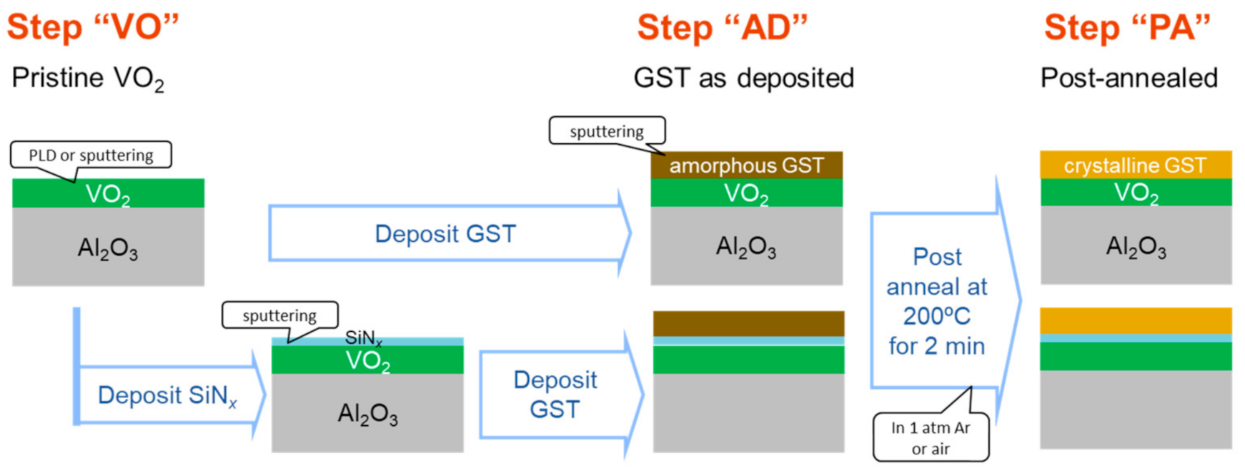
2.1. Sample Preparation
2.2. Characterization
3. Results
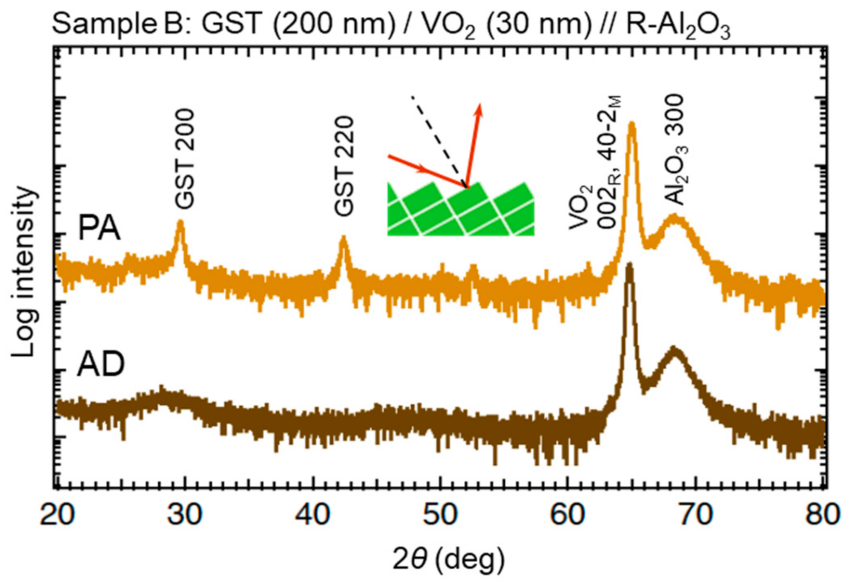
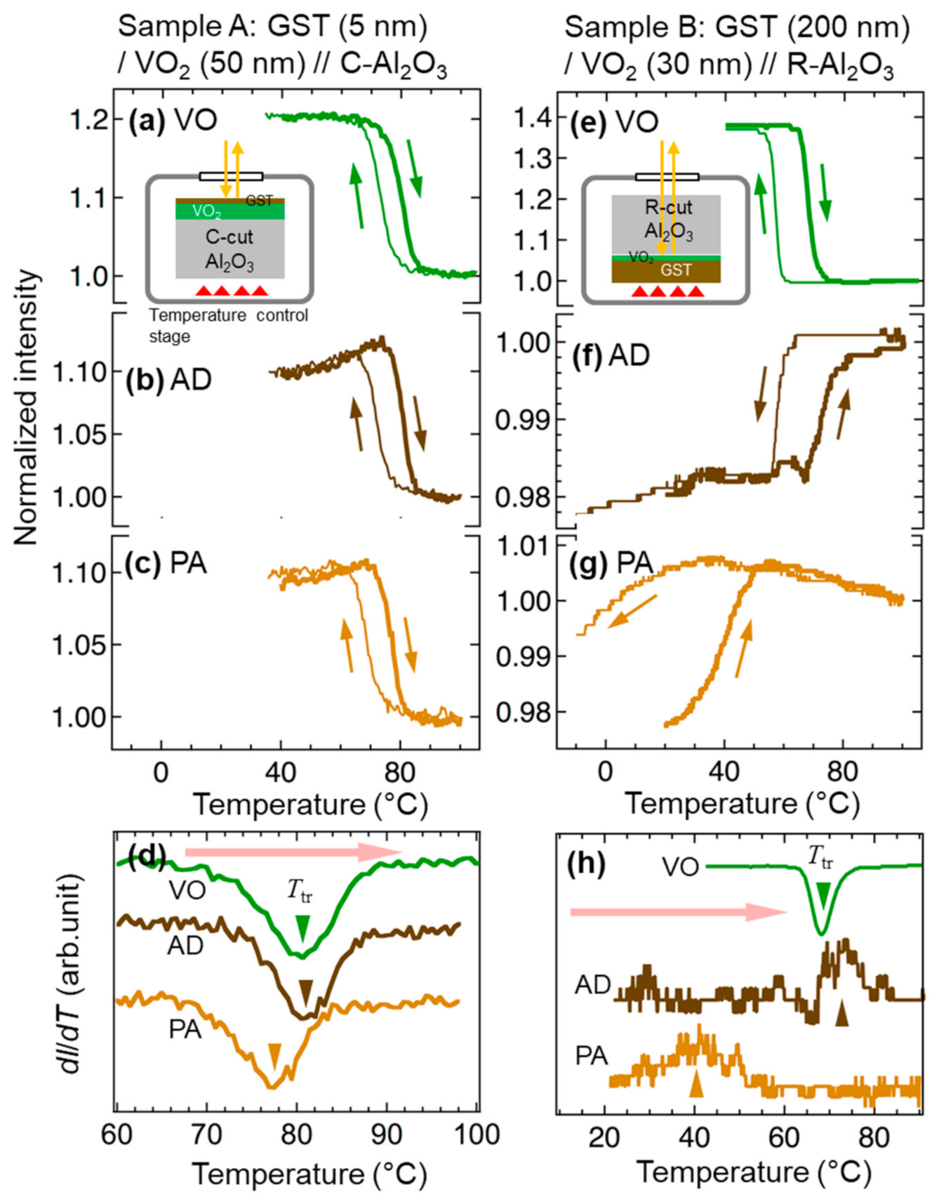
3.1. Optical Reflection
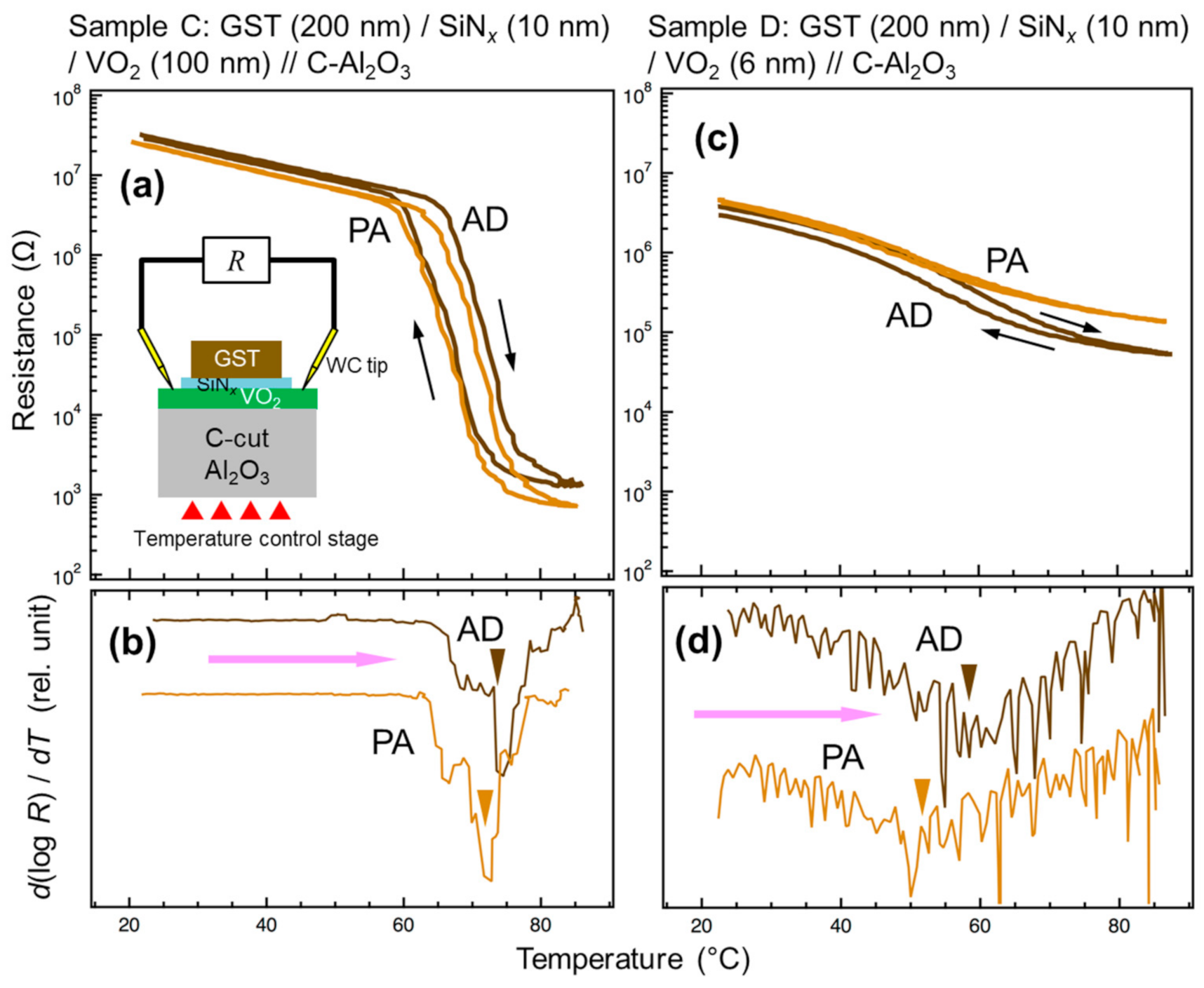
3.2. Electrical Resistance
4. Discussion
5. Conclusions
Author Contributions
Funding
Acknowledgments
Conflicts of Interest
References
- Morin, F.J. Oxides Which Show a Metal-to-Insulator Transition at the Neel Temperature. Phys. Rev. Lett. 1959, 3, 34–36. [Google Scholar] [CrossRef]
- Westman, S.; Lindqvist, I.; Sparrman, B.; Nielsen, G.B.; Nord, H.; Jart, A. Note on a Phase Transition in VO2. Acta Chem. Scand. 1961, 15, 217. [Google Scholar] [CrossRef]
- Van Steensel, K.; van de Burg, F.; Kooy, C. Thin-film switching elements of VO2. Philips Res. Repts. 1967, 22, 170–177. [Google Scholar]
- Berglund, C.; Walden, R. A thin-film inductance using thermal filaments. IEEE Trans. Electron. Devices 1970, 17, 137–148. [Google Scholar] [CrossRef]
- Cavalleri, A.; Tóth, C.; Siders, C.W.; Squier, J.A.; Ráksi, F.; Forget, P.; Kieffer, J.C. Femtosecond Structural Dynamics in VO2 during an Ultrafast Solid-Solid Phase Transition. Phys. Rev. Lett. 2001, 87, 237401. [Google Scholar] [CrossRef] [Green Version]
- Baum, P.; Yang, D.-S.; Zewail, A.H. 4D Visualization of Transitional Structures in Phase Transformations by Electron Diffraction. Science 2007, 318, 788–792. [Google Scholar] [CrossRef]
- Cao, J.; Gu, Y.; Fan, W.; Chen, L.Q.; Ogletree, D.F.; Chen, K.; Tamura, N.; Kunz, M.; Barrett, C.; Seidel, J.; et al. Extended Mapping and Exploration of the Vanadium Dioxide Stress-Temperature Phase Diagram. Nano Lett. 2010, 10, 2667–2673. [Google Scholar] [CrossRef]
- Pellegrino, L.; Manca, N.; Kanki, T.; Tanaka, H.; Biasotti, M.; Bellingeri, E.; Siri, A.S.; Marré, D. Multistate memory devices based on free-standing VO2/TiO2 microstructures driven by Joule self-heating. Adv. Mater. 2012, 24, 2929–2934. [Google Scholar] [CrossRef]
- Bae, S.-H.; Lee, S.; Koo, H.; Lin, L.; Jo, B.H.; Park, C.; Wang, Z.L. The Memristive Properties of a Single VO2 Nanowire with Switching Controlled by Self-Heating. Adv. Mater. 2013, 25, 5098–5103. [Google Scholar] [CrossRef]
- Jeong, J.; Aetukuri, N.; Graf, T.; Schladt, T.D.; Samant, M.G.; Parkin, S.S.P. Suppression of Metal-Insulator Transition in VO2 by Electric Field-Induced Oxygen Vacancy Formation. Science 2013, 339, 1402–1405. [Google Scholar] [CrossRef]
- Muraoka, Y.; Hiroi, Z. Metal—Insulator transition of VO2 thin films grown on TiO2 (001) and (110) substrates. Appl. Phys. Lett. 2002, 80, 583–585. [Google Scholar] [CrossRef] [Green Version]
- Fan, L.L.; Chen, S.; Luo, Z.L.; Liu, Q.H.; Wu, Y.F.; Song, L.; Ji, D.X.; Wang, P.; Chu, W.S.; Gao, C.; et al. Strain dynamics of ultrathin VO2 film grown on TiO2 (001) and the associated phase transition modulation. Nano Lett. 2014, 14, 4036–4043. [Google Scholar] [CrossRef] [PubMed]
- Kim, H.; Charipar, N.; Figueroa, J.; Bingham, N.S.; Piqué, A. Control of metal-insulator transition temperature in VO2 thin films grown on RuO2/TiO2 templates by strain modification. AIP Adv. 2019, 9, 015302. [Google Scholar] [CrossRef] [Green Version]
- Jia, Q.; Grenzer, J.; He, H.; Anwand, W.; Ji, Y.; Yuan, Y.; Huang, K.; You, T.; Yu, W.; Ren, W.; et al. 3D Local Manipulation of the Metal-Insulator Transition Behavior in VO2 Thin Film by Defect-Induced Lattice Engineering. Adv. Mater. Interfaces 2018, 5. [Google Scholar] [CrossRef]
- Gu, D.-E.; Zheng, H.; Ma, Y.; Xu, S.; Zhou, X. A highly-efficient approach for reducing phase transition temperature of VO2 polycrystalline thin films through Ru4+-doping. J. Alloys Compd. 2019, 790, 602–609. [Google Scholar] [CrossRef]
- Molegraaf, H.J.A.; Hoffman, J.; Vaz, C.A.F.; Gariglio, S.; Van Der Marel, D.; Ahn, C.H.; Triscone, J.-M. Magnetoelectric Effects in Complex Oxides with Competing Ground States. Adv. Mater. 2009, 21, 3470–3474. [Google Scholar] [CrossRef]
- Zheng, R.K.; Wang, Y.; Liu, Y.K.; Gao, G.Y.; Fei, L.F.; Jiang, Y.; Chan, H.L.W.; Li, X.M.; Luo, H.S.; Li, X.G. Epitaxial growth and interface strain coupling effects in manganite film/piezoelectric-crystal multiferroic heterostructures. Mater. Chem. Phys. 2012, 133, 42–46. [Google Scholar] [CrossRef]
- Leufke, P.M.; Kruk, R.; Brand, R.A.; Hahn, H. In situ magnetometry studies of magnetoelectric LSMO/PZT heterostructures. Phys. Rev. B 2013, 87, 094416. [Google Scholar] [CrossRef]
- Zhang, S.; Zhao, Y.G.; Li, P.S.; Yang, J.J.; Rizwan, S.; Zhang, J.X.; Seidel, J.; Qu, T.L.; Yang, Y.J.; Luo, Z.L.; et al. Electric-field control of nonvolatile magnetization in Co40Fe40B20/Pb(Mg1/3Nb2/3)0.7Ti0.3O3 structure at room temperature. Phys. Rev. Lett. 2012, 108, 137203. [Google Scholar] [CrossRef]
- Brandlmaier, A.; Geprägs, S.; Woltersdorf, G.; Gross, R.; Goennenwein, S.T.B. Nonvolatile, reversible electric-field controlled switching of remanent magnetization in multifunctional ferromagnetic/ferroelectric hybrids. J. Appl. Phys. 2011, 110, 043913. [Google Scholar] [CrossRef] [Green Version]
- Chen, A.T.; Zhao, Y. Research Update: Electrical manipulation of magnetism through strain-mediated magnetoelectric coupling in multiferroic heterostructures. APL Mater. 2016, 4, 032303. [Google Scholar] [CrossRef]
- Sakai, J.; Bavencoffe, M.; Negulescu, B.; Limelette, P.; Wolfman, J.; Tateyama, A.; Funakubo, H. Strain-induced resistance change in V2O3 films on piezoelectric ceramic disks. J. Appl. Phys. 2019, 125, 115102. [Google Scholar] [CrossRef] [Green Version]
- Petraru, A.; Soni, R.; Kohlstedt, H. Voltage controlled biaxial strain in VO2 films grown on 0.72Pb(Mg1/3Nb2/3)-0.28PbTiO3 crystals and its effect on the transition temperature. Appl. Phys. Lett. 2014, 105, 092902. [Google Scholar] [CrossRef]
- Nan, T.; Liu, M.; Ren, W.; Ye, Z.G.; Sun, N.X. Voltage control of metal-insulator transition and non-volatile ferroelastic switching of resistance in VOx/PMN-PT Heterostructures. Sci. Rep. 2014, 4, 5931. [Google Scholar] [CrossRef] [Green Version]
- Zhi, B.; Gao, G.; Xu, H.; Chen, F.; Tan, X.; Chen, P.; Wang, L.; Wu, W. Electric-field-modulated nonvolatile resistance switching in VO2/PMN-PT (111) heterostructures. Appl. Mater. Interfaces 2014, 6, 4603–4608. [Google Scholar] [CrossRef] [Green Version]
- Zhang, J.; Kong, W.; Liu, L.; Li, C.; Fang, L.; Feng, Y.P.; Tang, R.; Su, X.; Chen, J. Piezoelectric control of resistance switching in VO2/Pb(Zr0.52Ti0.48)O3 heterostructure. Appl. Phys. Lett. 2019, 114, 061603. [Google Scholar] [CrossRef]
- Verdaguer, A.; López-Mir, L.; Paradinas, M.; Holý, V.; Železný, J.; Yi, D.; Suresha, S.J.; Liu, J.; Serrao, C.R.; Ramesh, R.; et al. Giant reversible nanoscale piezoresistance at room temperature in Sr2IrO4 thin films. Nanoscale 2015, 7, 3453–3459. [Google Scholar] [CrossRef] [Green Version]
- Alyabyeva, N.; Sakai, J.; Bavencoffe, M.; Wolfman, J.; Limelette, P.; Funakubo, H.; Ruyter, A. Metal-insulator transition in V2O3 thin film caused by tip-induced strain. Appl. Phys. Lett. 2018, 113, 241603. [Google Scholar] [CrossRef]
- Kuwahara, M.; Suzuki, O.; Taketoshi, N.; Yamakawa, Y.; Yagi, T.; Fons, P.; Tsutsumi, K.; Suzuki, M.; Fukaya, T.; Tominaga, J.; et al. Measurements of Temperature Dependence of Optical and Thermal Properties of Optical Disk Materials. Jpn. J. Appl. Phys. 2006, 45, 1419–1421. [Google Scholar] [CrossRef]
- Kuwahara, M.; Suzuki, O.; Yamakawa, Y.; Taketoshi, N.; Yagi, T.; Fons, P.; Fukaya, T.; Tominaga, J.; Baba, T. Temperature Dependence of the Thermal Properties of Optical Memory Materials. Jpn. J. Appl. Phys. 2007, 46, 3909–3911. [Google Scholar] [CrossRef]
- Endo, R.; Maeda, S.; Jinnai, Y.; Lan, R.; Kuwahara, M.; Kobayashi, Y.; Susa, M. Electric Resistivity Measurements of Sb2Te3 and Ge2Sb2Te5 Melts Using Four-Terminal Method. Jpn. J. Appl. Phys. 2010, 49. [Google Scholar] [CrossRef]
- Hada, M.; Oba, W.; Kuwahara, M.; Katayama, I.; Saiki, T.; Takeda, J.; Nakamura, K.G. Ultrafast time-resolved electron diffraction revealing the nonthermal dynamics of near-UV photoexcitation-induced amorphization in Ge2Sb2Te5. Sci. Rep. 2015, 5, 13530. [Google Scholar] [CrossRef] [PubMed] [Green Version]
- Ikuma, Y.; Shoji, Y.; Kuwahara, M.; Wang, X.; Kintaka, K.; Kawashima, H.; Tanaka, D.; Tsuda, H. Small-sized optical gate switch using Ge2Sb2Te5 phase-change material integrated with silicon waveguide. Electron. Lett. 2010, 46, 368. [Google Scholar] [CrossRef]
- Tanaka, D.; Ikuma, Y.; Shoji, Y.; Kuwahara, M.; Wang, X.; Kintaka, K.; Kawashima, H.; Toyosaki, T.; Tsuda, H. Demonstration of 1000-times switching of phase-change optical gate with Is wire waveguides. Electron. Lett. 2011, 47, 268–269. [Google Scholar] [CrossRef]
- Tanaka, D.; Shoji, Y.; Kuwahara, M.; Wang, X.; Kintaka, K.; Kawashima, H.; Toyosaki, T.; Ikuma, Y.; Tsuda, H. Ultra-small, self-holding, optical gate switch using Ge2Sb2Te5 with a multi-mode Si waveguide. Opt. Express 2012, 20, 10283–10294. [Google Scholar] [CrossRef]
- Moriyama, T.; Tanaka, D.; Jain, P.; Kawashima, H.; Kuwahara, M.; Wang, X.; Tsuda, H. Ultra-compact, self-holding asymmetric Mach-Zehnder interferometer switch using Ge2Sb2Te5 phase-change material. IEICE Electron. Express 2014, 11, 20140538. [Google Scholar] [CrossRef] [Green Version]
- Kato, K.; Kuwahara, M.; Kawashima, H.; Tsuruoka, T.; Tsuda, H. Current-driven phase-change optical gate switch using indium—Tin-oxide heater. Appl. Phys. Express 2017, 10, 072201. [Google Scholar] [CrossRef]
- Njoroge, W.K.; Wöltgens, H.-W.; Wuttig, M. Density changes upon crystallization of Ge2Sb2.04Te4.74 films. J. Vac. Sci. Technol. A 2002, 20, 230–233. [Google Scholar] [CrossRef]
- Nagashima, K.; Yanagida, T.; Tanaka, H.; Kawai, T. Influence of ambient atmosphere on metal-insulator transition of strained vanadium dioxide ultrathin films. J. Appl. Phys. 2006, 100, 063714. [Google Scholar] [CrossRef]
- Meng, Y.; Behera, J.K.; Ke, Y.; Chew, L.; Wang, Y.; Long, Y.; Simpson, R.E. Design of a 4-level active photonics phase change switch using VO2 and Ge2Sb2Te5. Appl. Phys. Lett. 2018, 113, 071901. [Google Scholar] [CrossRef]
- Hu, Y.; Zou, H.; Zhang, J.; Xue, J.; Sui, Y.; Wu, W.; Yuan, L.; Zhu, X.; Song, S.; Song, Z. Ge2Sb2Te5/Sb superlattice-like thin fil for high speed change memory application. Appl. Phys. Lett. 2015, 107, 263105. [Google Scholar] [CrossRef]
- Sakai, J.; Kuwahara, M.; Hotsuki, M.; Katano, S.; Uehara, Y. Selective scanning tunneling microscope light emission from rutile phase of VO2. J. Phys. Condens. Matter 2016, 28, 385002. [Google Scholar] [CrossRef] [PubMed]
- Azhan, N.H.; Su, K.; Okimura, K.; Zaghrioui, M.; Sakai, J. Appearance of large crystalline domains in VO2 films grown on sapphire (001) and their phase transition characteristics. J. Appl. Phys. 2015, 117, 245314. [Google Scholar] [CrossRef]
- Kurosawa, K.; Pierce, R.M.; Ushioda, S.; Hemminger, J.C. Raman scattering and attenuated-total-reflection studies of surface-plasmon polaritons. Phys. Rev. B 1986, 33, 789–798. [Google Scholar] [CrossRef] [PubMed]
- Philipp, H.R. Silicon dioxide (SiO2) (Glass). In Handbook of Optical Constants of Solids; Palik, E.D., Ed.; Academic Press: New York, NY, USA, 1985; p. 749. [Google Scholar]
- Lamsal, C.; Ravindra, N.M. Optical properties of vanadium oxides-an analysis. J. Mater. Sci. 2013, 48, 6341–6351. [Google Scholar] [CrossRef]
- Krammer, A.; Magrez, A.; Vitale, W.A.; Mocny, P.; Jeanneret, P.; Guibert, E.; Whitlow, H.J.; Ionescu, A.M.; Schüler, A. Elevated transition temperature in Ge doped VO2 thin films. J. Appl. Phys. 2017, 122, 045304. [Google Scholar] [CrossRef] [Green Version]
- Liu, S.-J.; Su, Y.-T.; Hsieh, J.-H. Effects of postdeposition annealing on the metal–insulator transition of VO2−x thin films prepared by RF magnetron sputtering. Jpn. J. Appl. Phys. 2014, 53, 33201. [Google Scholar] [CrossRef]
- Zhang, J.; Zhao, Z.; Li, J.; Jin, H.; Rehman, F.; Chen, P.; Jiang, Y.; Chen, C.; Cao, M.; Zhao, Y. Evolution of Structural and Electrical Properties of Oxygen-Deficient VO2 under Low Temperature Heating Process. ACS Appl. Mater. Interfaces 2017, 9, 27135–27141. [Google Scholar] [CrossRef]
- Uchino, K. Electrostrictive actuators: Materials and applications. Am. Ceram. Soc. Bull. 1986, 65, 647–652. [Google Scholar]
- Marchant, A.B. Optical Recording: A Technical Overview; Addison-Wesley Publishing: Boston, MA, USA, 1990; pp. 84–88. [Google Scholar]

| Sample | VO2 Thickness (nm) | GST Thickness (nm) | SiNx Layer | Substrate | AD | PA | ||
|---|---|---|---|---|---|---|---|---|
| Meas. | Ttr (°C) | Meas. | Ttr (°C) | |||||
| A | 50 | 5 | No | C-cut Al2O3 | Refl. | 81 | Refl. | 77 |
| B | 30 | 200 | No | R-cut Al2O3 | Refl. | 72 | Refl. | 41 |
| C | 100 | 200 | Yes | C-cut Al2O3 | R–T | 74 | R–T | 72 |
| D | 6 | 200 | Yes | C-cut Al2O3 | R–T | 58 | R–T | 52 |
Publisher’s Note: MDPI stays neutral with regard to jurisdictional claims in published maps and institutional affiliations. |
© 2020 by the authors. Licensee MDPI, Basel, Switzerland. This article is an open access article distributed under the terms and conditions of the Creative Commons Attribution (CC BY) license (http://creativecommons.org/licenses/by/4.0/).
Share and Cite
Sakai, J.; Kuwahara, M.; Okimura, K.; Uehara, Y. Stress-Induced In Situ Modification of Transition Temperature in VO2 Films Capped by Chalcogenide. Materials 2020, 13, 5541. https://doi.org/10.3390/ma13235541
Sakai J, Kuwahara M, Okimura K, Uehara Y. Stress-Induced In Situ Modification of Transition Temperature in VO2 Films Capped by Chalcogenide. Materials. 2020; 13(23):5541. https://doi.org/10.3390/ma13235541
Chicago/Turabian StyleSakai, Joe, Masashi Kuwahara, Kunio Okimura, and Yoichi Uehara. 2020. "Stress-Induced In Situ Modification of Transition Temperature in VO2 Films Capped by Chalcogenide" Materials 13, no. 23: 5541. https://doi.org/10.3390/ma13235541