Article

Electronic Structure and Surface Properties of Copper Thiocyanate: A Promising Hole Transport Material for Organic Photovoltaic Cells

1
Department of Theoretical and Applied Physics, African University of Science and Technology, Km 10 Airport Road, Galadimawa, Abuja F.C.T. 900107, Nigeria
2
Department of Nanoscience and Nanotechnology, University of Grenoble Alpes, CS 40700 Grenoble, France
3
Department of Material Science and Engineering, African University of Science and Technology, Km 10 Airport Road, Galadimawa, Abuja F.C.T. 900107, Nigeria
4
School of Chemistry, Cardiff University, Main Building, Cardiff CF10 3AT, UK
*
Author to whom correspondence should be addressed.
Materials 2020, 13(24), 5765; https://doi.org/10.3390/ma13245765
Submission received: 19 November 2020 / Revised: 10 December 2020 / Accepted: 14 December 2020 / Published: 17 December 2020

Abstract

:
Considering the significance of hexagonal copper thiocyanate (β-CuSCN) in several optoelectronic technologies and applications, it is essential to investigate its electronic structure and surface properties. Herein, we have employed density functional theory (DFT) calculations to characterise the band structure, density of states, and the energy-dependent X-ray photoelectron (XPS) valence band spectra at variable excitation energies of β-CuSCN. The surface properties in the absence and presence of dimethyl sulfoxide (DMSO), a solvent additive for improving perovskite solar cells’ power conversion efficiency, have also been systematically characterised. β-CuSCN is shown to be an indirect band gap material (Eg = 3.68 eV) with the valence band edge demonstrated to change from being dominated by Cu-3d at soft X-ray ionisation photon energies to Cu-3p at hard X-ray ionisation photon energies. The adsorption energy of dimethyl sulfoxide (DMSO) on the (100) and (110) β-CuSCN surfaces is calculated at −1.12 and −0.91 eV, respectively. The presence of DMSO on the surface is shown to have a stabilisation effect, lowering the surface energy and tuning the work function of the β-CuSCN surfaces, which is desirable for organic solar cells to achieve high power conversion efficiencies.

Graphical Abstract

1. Introduction

Halide perovskite solar cells (PSCs) are attractive, cost-effective, and earth-abundant candidates for solar cell development [1,2,3]. Because of the distinctive physical and optoelectronic properties, the organic–inorganic halide perovskites with typical ABX3 formula have attained certified overall conversion efficiencies exceeding 22% [4,5,6], making these materials suitable candidates to replace commonly employed Si-based solar cells. Perovskite solar cell device architecture consists of three important layers: the active photoabsorber (halide perovskite) layer, a hole-transporting layer (HTL), and an electron-transporting layer (ETL), to extract holes and electrons, respectively.
The hole-transporting layer helps to achieve efficient separation and transport of electrons and holes, which is essential for achieving high-performing perovskite solar cells. A large internal surface area of the active n-type photoabsorber layer can be used when pores in it can be filled entirely with a p-type HTL layer [7]. Although Spiro-OMeTAD is one of the most widely utilised HTL materials in PSCs [8], its instability limits peak performance attainment [9,10,11,12,13]. Tailored poly(3,4-ethylenedioxythiophene) polystyrene sulfonate (PEDOT:PSS) is another commonly used HTL material for high-efficiency perovskite solar cells [14,15,16,17]. Despite its many desirable properties, the sensitivity of the surface properties, including the work function, to processing conditions remain major challenges of PEDOT: PSS [18,19,20].
Copper(I) thiocyanate (CuSCN) is one of the promising hole-transporting p-type semiconductors owing to its chemical stability, nontoxicity, low-cost, high visible light transparency, and high hole conductivity (≥5 × 10⁻⁴ Scm−1) [21,22,23,24]. CuSCN can also be easily synthesised at high purities and it can be chemically modified because of its quasimolecular nature [25,26]. Due to its ability to effectively fill the pores/cracks in active n-type absorber layers, CuSCN can promote efficient transport of photogenerated carriers [7,27,28,29,30]. By using CuSCN as the hole extraction layer, Arora et al. achieved not only excellent thermal stability but also high stabilised efficiency exceeding 20% [21]. CuSCN has also attracted a surge of interest in light-emitting diodes (LEDs) [31,32], photodetectors [33,34], and field-effect transistors (FETs) [35].
Owing to the relevance of CuSCN to several critical technological applications, the fundamental electronic structure and surface properties must be comprehensively characterised and understood. This work presents a density functional theory (DFT) characterisation of the electronic structures: band structure, density of states (DOS), and X-ray photoelectron (XPS) valence band spectra at variable excitation energies of β-CuSCN. The simulated valence band spectra are compared with photoelectron spectroscopy measurements, which provide information on the electronic structure. Although DFT calculated density of states (DOS) have been used to interpret experimentally measured valence photoelectron spectra of β-CuSCN [36], there is a clear limitation as the orbital energies obtained from first principles DFT calculations are not excitation energies. There is, therefore, the need to determine the valence band spectra of β-CuSCN at variable excitation energies that are comparable to those of conventional X-ray sources (e.g., Al Kα) and hard X-ray photoemission spectroscopy, which are more bulk-sensitive. The valence band edge of β-CuSCN is indeed shown in the present study to change from being dominated by Cu-3d at soft X-ray ionisation photon energies to Cu-3p at hard X-ray ionisation photon energies. The surface properties of β-CuSCN with and without dimethyl sulfoxide (DMSO) modification are characterised by determining the most stable adsorption geometries of DMSO on the most stable (100) and (110) β-CuSCN surfaces and investigating the adsorption effects on tuning the surface work function. A wide range of work function tuning is essential for obtaining a good energy level alignment between the β-CuSCN HTL and the absorber perovskite material, and hence improved device characteristics.

2. Materials and Methods

The DFT calculations were performed in the VASP—Vienna Ab initio Simulation Package [37,38,39]. The interactions between the valence and core electrons are described using the projected augmented wave (PAW) method [40]. The Perdew–Burke–Ernzerhof (PBE) exchange-correlation function is used for geometry optimisations [41]. To accurately predict the electronic band gap and density of states (DOS) features of CuSCN, the screened hybrid functional HSE06 [42] with an exchange value of 25% was used. A kinetic energy cut-off of 600 eV and Monkhorst-Pack [43] K-points mesh of 7 × 5 × 3 converge the total energy of β-CuSCN to within 10−6 eV, and the residual forces on all relaxed atoms reached 10−3 eVÅ−1.
The METADISE code [44] was used to create the (100) and (110) β-CuSCN surfaces. The stability of the surfaces is quantified by calculating the surface energy (γr) of the relaxed naked surfaces as:
γ r = E s u r f r e l a x e d n E b u l k 2 A
where E s u r f r e l a x e d     is the total energy of the relaxed surface, n E b u l k is the energy of an equal number (n) of the bulk β-CuSCN atoms, and A is the surface area. To avoid interactions between periodic slabs, a 20 Å vacuum is added to the c-direction. To ascertain whether the adsorption of DMSO has a stabilisation effect on the surface, we have also computed surface energy of the one-side (1 × A) DMSO-covered β-CuSCN surface, calculated as:
γ D M S O = E s u r f + D M S O r e l a x e d E D M S O n E b u l k A E s u r f r e l a x e d n E b u l k 2 A
where E s u r f + D M S O r e l a x e d   is the total energy of the DMSO-covered surface and   E D M S O   is the total energy of the free DMSO molecule. The adsorption energy (Eads) of DMSO on β-CuSCN surfaces is calculated as:
E a d s = E s u r f + D M S O r e l a x e d E s u r f r e l a x e d + E D M S O
Negative or positive adsorption energy denotes an exothermic or endothermic adsorption process, respectively. The averaged electrostatic potential along the c-direction of the (100) and (110) β-CuSCN surfaces was determined using the MacroDensity package [45,46]. The work function (Φ), the minimum energy required to eject an electron from a solid into vacuum, is determined as: Φ = EV − EF, where Ev is the vacuum level and EF is the Fermi level. Dipole corrections were accounted for in all surface calculations to ensure accurate determination of the vacuum level’s potential [47]. The XPS valence band spectra were simulated using the GALORE code [48], which used the Gelius model [49,50] to apply weightings to the atomic projected density of states (PDOS) based on the photoionisation cross-sections formulated by Scofield [51,52].

3. Results and Discussion

3.1. Crystal Structure β-CuSCN

CuSCN crystallises in two polymorphic forms, α-CuSCN (orthorhombic crystal lattice) and the β-CuSCN (hexagonal crystal structure) [53]. In the more stable β-CuSCN structure (Figure 1), the plains of Cu atoms are separated by layers of SCN ions, three-dimensionally interconnected by strong Cu–S bonds. As shown in Table 1, the lattice parameters of β-CuSCN are predicted at a = b = 3.828 Å and c = 10.970 Å, in close agreement with experimental data (a = b = 3.850 Å and c = 10.938 Å) [51] and previous DFT calculation results [36,54,55]. The average Cu–N, Cu–S, C–S, and C–N bond distances are calculated at 1.887, 2.316, 1.175, and 1.660 Å, respectively. The α(CuSC) and α(CuSCu) bond angles are predicted at 109.2° and 109.7°, respectively.

3.2. Electronic Properties of β-CuSCN

β-CuSCN has an indirect band gap of 3.68 eV, as evident in the band structure (Figure 2a). The hybrid HSE06 functional predicted band gap compares closely with commonly reported experimental values in the range of 3.6–3.9 eV [56,57,58,59] and previous theoretical calculations [36,54,55]. The partial density of states (PDOS) of β-CuSCN is shown in Figure 2b. The valence band maximum (VBM) is dominated by Cu-3d and S-2p states, whereas conduction band minimum (CBM) is composed mainly of C-2p and N-2p, with a small contribution from C-3d. To gain insight into the superior hole-transport property of β-CuSCN, we have computed the effective masses of holes ( m h * ) and electrons ( m e * ) by fitting a quadratic polynomial to the energy versus reciprocal lattice vector k: m e h * = ±   2 d 2 E k d k 2 1 . As shown in Table 2, the predicted m h * (at the valence band maximum) and m e * (at the conduction band minimum) in the Brillouin zone’s selected directions are generally very small, which point to their superior transport. The smallest effective masses of holes ( m h * ) appear in the direction from Γ to A (0.0037), whereas the highest appears in the Γ−M (0.1756) direction. These suggest that photogenerated holes in β-CuSCN should be easiest to transport along the Γ−A direction and least mobile in the Γ−M direction.
The energy-dependent XPS valence band spectra of β-CuSCN at variable excitation energies (Al Kα1 (1486 eV), 4068 eV, and 8133 eV), obtained by applying weightings to the DFT-PDOS using the Scofield [51] formulated photoionisation cross-sections are shown in Figure 3. The chosen photon energies correspond to moving from soft (1486 eV) to intermediate (4068 eV) to hard (8133 eV) X-ray ionisation photon energy (hν). Five spectral features are assigned: I for the main valence band region (onset from 0.0 eV and extends to 3.4 eV), II, III, IV, and V for the broad satellite features located around 4, 9, 17, and 21 eV binding energies, respectively. The intensity of I relative to IV and V decreases continuously for increasing photon energy, which resulted in modifying the main valence band spectrum’s shape and increasing the broad satellite features’ relative intensity. The changes in the valence band spectral features may be attributed to the photon energy dependence of the photoionisation cross-section to the photon energy dependence of the photoionisation cross-section of the atomic s, p, and d orbitals that contributes to the valence band. Cu-3d states dominate the main valence band region (I) for β-CuSCN at lower photon energies, owing to their higher photoionisation cross-section (Figure 3d). The Cu-3d photoionisation cross-section decreases much more rapidly than Cu-3p with increasing photon energy, so its contribution becomes less significant (Figure 3a–c). This resulted in the main valence band (I and II) switching from being dominated by Cu-3d to Cu-3p. The satellite broad-feature IV can be assigned to the main contribution from S-3s, whereas the broad-feature V is assigned to contributions from N-2s. The simulated main valance band features at soft X-ray ionisation photon energy (1.486 keV) shows good agreement with the XPS valence band spectrum of CuSCN thin films reported by Jaffe et al. [36], which demonstrate that Cu-3d states dominate the main valence band region for β-CuSCN at lower photon energies. These results are also consistent with the work of Wijeyasinghe et al. [57], who showed that Cu-3d peaks dominate the main valence band.

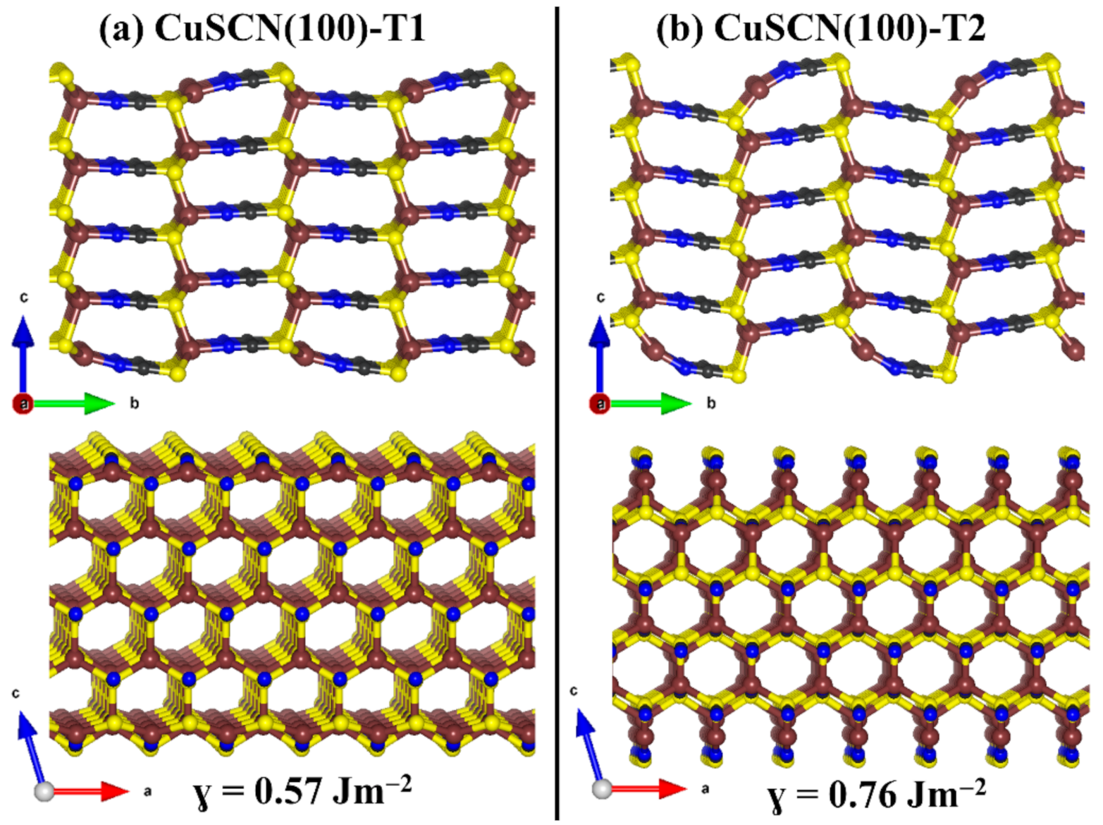
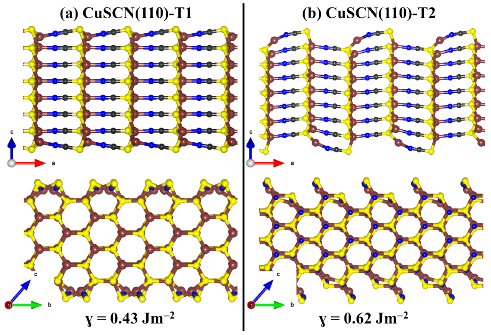
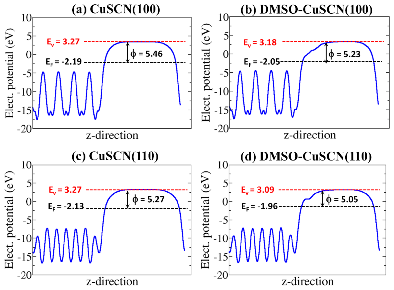
3.3. Surface Properties

Here, we have characterised the structure, composition, relative stabilities, and work function of the two most stable β-CuSCN (100) and (110) surfaces. Both surfaces have two non-dipolar terminations (denoted as termination T1 and T2), both of which are characterised to determine the most stable one. Shown in Figure 4 and Figure 5 are the relaxed structures of the two terminations of the (100) and (110) β-CuSCN surfaces. Termination T1 (T2) of the (100) surface has a calculated surface energy of 0.57 (0.76 Jm−2), indicating that the termination T1 is more stable than termination T2. Similarly, we predict the surface energy of T1 (T2) of the (110) surface to be 0.43 (0.62 Jm−2). Similarly, results were reported by Chen et al. [54], who reported surface energy of 0.74 and 0.63 Jm−2 for the most stable terminations of the (110) and (100) surfaces, respectively.
Next, we investigated the adsorption characteristics of dimethyl sulfoxide (DMSO) on the most T1 termination of the β-CuSCN (100) and (110) surfaces to ascertain adsorption effects on the surface stability and work function. These insights are essential, considering that residues of DMSO solvent that is typically used to fabricate solution-processable halide perovskite materials [60] may adsorb onto the HTL β-CuSCN surfaces, altering the electronic properties. The DMSO molecule is introduced to the (100) and (110) surfaces in different orientations and at various sites to predict the most stable adsorption geometries, as shown in Figure 6. At both surfaces, the DMSO interacts with the Cu sites through the O atom, releasing an adsorption of −1.12 and −0.91 eV at the (100) and (110) surfaces, respectively. The interacting Cu–O bond distance at the (100) surface is calculated at 2.126 Å, whereas at the (110) surface, it is 2.191 Å (Table 3). Our predicted adsorption structures and energetics of DMSO at the β-CuSCN (100) and (110) surfaces are in good agreement with those reported by Zhang and Chen et al. [61], who show that the solvent DMSO molecule exhibits reasonable interactions with the CuSCN surfaces, predicting adsorption energy of 1.28 and 0.84 eV at the (001) and (110) surfaces, respectively.
The adsorption of the DMSO on the (100) and (110) surfaces is demonstrated to be characterised by redistribution of charge density in the surface-DMSO systems, as obtained from analysis of the differential charge density ( ρ ) iso-surface contours (Figure 6c,d). ρ = ρ s u r f + D M S O ρ s u r f + ρ D M S O , where ρ s u r f + D M S O ,   ρ s u r f , and ρ D M S O are the charge density of the total surf-DMSO complex, the naked β-CuSCN surface, and the free DMSO molecule as in the relaxed adsorbed configuration. We observe charge density accumulation between the Cu–O bonds, suggesting chemisorption. Bader charge analyses reveal that the net charge transfer from the β-CuSCN surfaces to the DMSO molecule is minimal, calculated to be 0.08 and 0.05 e at the (100) and (110) surfaces, respectively (Table 3). Owing to the small charge transfer to the DMSO molecule upon adsorption, the interatomic bond distances and angles changed marginally, relative to the gas-phase parameters.
The DMSO-covered surfaces are predicted to have smaller surface energies compared to the naked surfaces, suggesting that the DMSO adsorption has a stabilisation effect on the (100) and (110) β-CuSCN surfaces. The DMSO-covered β-CuSCN(100) surface energy is calculated at 0.49 Jm-2, compared to 0.57 Jm−2 for the naked surface. Similarly, the DMSO-covered β-CuSCN (110) surface has a surface energy of 0.39 Jm−2, compared to 0.43 Jm−2 for the naked surface. The adsorption of DMSO on the (100) and (110) β-CuSCN surfaces modifies their work function (Φ). Hole transport materials with a high degree of tunable work functions that permit proper energy alignment with the donor materials’ deep valence bands are desirable for high-efficiency organic solar cells [62]. The Φ of the naked CuSCN (100) surface is computed at 5.46 eV vs. vacuum, as shown in Figure 7a, compared to 5.23 eV for the DMSO-covered (100) surface (Figure 7b). For the CuSCN (110) surface, the Φ naked and DMSO-covered surfaces are predicted at 5.27 and 5.05 eV, respectively (Figure 7c,d).
The reduction in the work function upon DMSO adsorption may be rationalised by considering the fact that the DMSO adsorption is characterised by electron density rearrangement, which smoothens the surface electric charge distribution according to the Smoluchowski effect [63,64]. Similar results have been reported for other organic functionalised surfaces [65,66,67,68]. These calculated work functions compare closely with experimental measurements, which report the Φ of CuSCN in the range of 5.0–5.4 eV [69,70,71,72]. Wijesekara et al. [70] reported the work function of CuSCN thick film to be 4.82 eV. Dzikri et al. [71] and Kim et al. [72] reported the work functions of 5.53 and 5.4 eV, respectively. The predicted work function of CuSCN also compares with those of other commonly used hole transport layer materials: Spiro-OMeTAD = 4.9, PEDOT:PSS = 5.1 eV, NiOx = 5.4 eV, V2O5 = 5.4 eV, MoOx = 5.3 eV, WO3 = 5.35 eV, and GO = 4.9 eV [73,74]. The close match between the work function of CuSCN and the highest occupied molecular orbital level of most perovskite materials (e.g., CH3NH3PbI3 = –5.4 eV) ensures good alignment of energy levels, which will give rise to improvements in device efficiency.

4. Summary and Conclusions

In summary, we have comprehensively characterised the electronic structure, energy-dependent XPS valence band spectra at variable excitation energies, and the surface properties of β-CuSCN in the absence and presence of dimethyl sulfoxide (DMSO), using first principles density functional theory calculations. The β-CuSCN is shown to possess an indirect large band gap (Eg = 3.68 eV) with the valence band edge demonstrated to change from being dominated by Cu-3d at soft photon energies to Cu-3p at hard X-ray ionisation photon energies. The adsorption of DMSO on the (100) and (110) β-CuSCN surfaces was demonstrated to have a stabilisation effect, lowering the surface energy. The adsorption was shown to be characterised by electron redistribution in the DMSO-CuSCN systems, leading to accumulation within the interacting Cu–O bonding regions. The presence of the DMSO was shown to tune the work function of the CuSCN surfaces, which is desirable for hole transport layer materials to achieve improved solar device characteristics and performance.

Author Contributions

B.A.O., G.D.C., J.A.F., K.S.S., D.K.T., A.R.T., T.C.B., and J.A.A. performed the DFT calculations and performed data analysis. N.Y.D. led the research and study design, performed data analysis, scientific discussion of the results, and wrote the paper. All authors have read and agreed to the published version of the manuscript.

Funding

This work is funded by the UK Engineering and Physical Sciences Research Council (EPSRC) for funding (Grant No. EP/S001395/1).

Acknowledgments

The simulations were performed using the computational facilities of the Advanced Research Computing @ Cardiff (ARCCA) Division, Cardiff University. This work also made use of the facilities of ARCHER (http://www.archer.ac.uk), the UK’s national supercomputing service via our membership of the UK’s HEC Materials Chemistry Consortium, which is funded by EPSRC (EP/L000202). Information on the data that underpins the results presented here, including how to access them, can be found in the Cardiff University data catalogue at http://doi.org/10.17035/d.2020.0124286506.

Conflicts of Interest

The authors declare no conflict of interest.

References

  1. Sidney, E.C.; Evan, N.; Michael, C.D.; Daniel, R.G. Colloidal nanocrystals of lead-free double-perovskite (elpasolite) semiconductors: Synthesis and anion exchange to access new materials. Nano Lett. 2018, 18, 1118–1123. [Google Scholar]
  2. Kojima, A.; Teshima, K.; Shirai, Y.; Miyasaka, T. Organometal Halide Perovskites as Visible-Light Sensitizers for Photovoltaic Cells. J. Am. Chem. Soc. 2009, 131, 6050–6051. [Google Scholar] [PubMed]
  3. Heo, J.H.; Im, S.H.; Noh, J.H.; Mandal, T.N.; Lim, C.-S.; Chang, J.A.; Lee, Y.H.; Kim, H.J.; Sarkar, A.; Nazeeruddin, M.K. Efficient inorganic–organic hybrid heterojunction solar cells containing perovskite compound and polymeric hole conductors. Nat. Photonics 2013, 7, 486–491. [Google Scholar]
  4. Green, M.A.; Ho-Baillie, A.; Snaith, H.J. The emergence of perovskite solar cells. Nat. Photonics 2014, 8, 506–514. [Google Scholar]
  5. National Renewable Energy Laboratory Service. Photovoltaic Research: Efficiency Chart. Available online: https://www.nrel.gov/pv/assets/images/efficiency-chart.png (accessed on 17 December 2020).
  6. Gao, L.; Yang, G. Organic-Inorganic Halide Perovskites: From Crystallization of Polycrystalline Films to Solar Cell Applications. Sol. RRL 2020, 4, 1900200. [Google Scholar]
  7. O’Regan, B.; Lenzmann, F.; Muis, R.; Wienke, J. A solid-state dye-sensitized solar cell fabricated with pressure-treated P25-TiO2 and CuSCN: Analysis of pore filling and IV characteristics. Chem. Mater. 2002, 14, 5023–5029. [Google Scholar]
  8. Yang, Y.; Hoang, M.T.; Yao, D.; Pham, N.D.; Tiong, V.T.; Wang, X.; Wang, H. Spiro-OMeTAD or CuSCN as a preferable hole transport material for carbon-based planar perovskite solar cells. Mater. Chem. A 2020, 8, 12723–12734. [Google Scholar]
  9. Ponseca, C.S.; Hutter, E.M.; Piatkowski, P.; Cohen, B.; Pascher, T.; Douhal, A.; Yartsev, A.; Sundström, V.; Savenije, T.J. Mechanism of Charge Transfer and Recombination Dynamics in Organo Metal Halide Perovskites and Organic Electrodes, PCBM, and Spiro-OMeTAD: Role of Dark Carriers. J. Am. Chem. Soc. 2015, 137, 16043–16048. [Google Scholar]
  10. Abrusci, A.; Stranks, S.D.; Docampo, P.; Yip, H.; Jen, A.K.-Y.; Snaith, H.J. High-Performance Perovskite-Polymer Hybrid Solar Cells via Electronic Coupling with Fullerene Monolayers. Nano Lett. 2013, 13, 3124–3128. [Google Scholar]
  11. Shariatinia, Z. Recent progress in development of diverse kinds of hole transport materials for the perovskite solar cells: A review. Renew. Sustain. Energy Rev. 2020, 119, 109608. [Google Scholar]
  12. Bi, D.; Tress, W.; Dar, M.I.; Gao, P.; Luo, J.; Renevier, C.; Schenk, K.; Abate, A.; Giordano, F.; Correa Baena, J.-P.; et al. Efficient Luminescent Solar Cells Based on Tailored Mixed-Cation Perovskites. Sci. Adv. 2016, 2, 1501170. [Google Scholar]
  13. Abate, A.; Hollman, D.J.; Teuscher, J.; Pathak, S.; Avolio, R.; D’Errico, G.; Vitiello, G.; Fantacci, S.; Snaith, H.J. Protic Ionic Liquids as P-Dopant for Organic Hole Transporting Materials and Their Application in High Efficiency Hybrid Solar Cells. J. Am. Chem. Soc. 2013, 135, 13538–13548. [Google Scholar] [PubMed]
  14. Reza, K.M.; Gurung, A.; Bahrami, B.; Mabrouk, S.; Elbohy, H.; Pathak, R.; Chen, K.; Chowdhury, A.H.; Rahman, M.T.; Letourneau, S.; et al. Tailored PEDOT:PSS hole transport layer for higher performance in perovskite solar cells: Enhancement of electrical and optical properties with improved morphology. J. Energy Chem. 2020, 44, 41–50. [Google Scholar]
  15. Syed, A.A.; Poon, C.Y.; Li, H.W.; Zhu, F. A sodium citrate-modified-PEDOT:PSS hole transporting layer for performance enhancement in inverted planar perovskite solar cells. J. Mater. Chem. C 2019, 7, 5260–5266. [Google Scholar]
  16. Huang, D.; Goh, T.; Kong, J.; Zheng, Y.; Zhao, S.; Xu, Z.; Taylor, A.D. Perovskite solar cells with a DMSO-treated PEDOT:PSS hole transport layer exhibit higher photovoltaic performance and enhanced durability. Nanoscale 2017, 9, 4236–4243. [Google Scholar] [PubMed]
  17. Yaacobi-Gross, N.; Treat, N.D.; Pattanasattayavong, P.; Faber, H.; Perumal, A.K.; Stingelin, N.; Bradley, D.D.C.; Stavrinou, P.N.; Heeney, M.; Anthopoulos, T.D. High-Efficiency Organic Photovoltaic Cells Based on the Solution-Processable Hole Transporting Interlayer Copper Thiocyanate (CuSCN) as a Replacement for PEDOT:PSS. Adv. Energy Mater. 2015, 5, 1401529. [Google Scholar]
  18. Huang, J.; Miller, P.F.; Wilson, J.S.; de Mello, A.J.; de Mello, J.C.; Bradley, D.D.C. Investigation of the Effects of Doping and Post-Deposition Treatments on the Conductivity, Morphology, and Work Function of Poly(3,4-ethylenedioxythiophene)/Poly(styrene sulfonate) Films. Adv. Funct. Mater. 2005, 15, 290–296. [Google Scholar]
  19. Nardes, A.M.; Kemerink, M.; de Kok, M.M.; Vinken, E.; Maturova, K.; Janssen, R.A. Conductivity, work function, and environmental stability of PEDOT:PSS thin films treated with sorbitol. Org. Electron. 2008, 9, 727–734. [Google Scholar]
  20. Im, S.G.; Gleason, K.K.; Olivetti, E.A. Doping level and work function control in oxidative chemical vapor deposited poly (3,4-ethylenedioxythiophene). Appl. Phys. Lett. 2007, 90, 152112. [Google Scholar]
  21. Arora, N.; Dar, M.I.; Hinderhofer, A.; Pellet, N.; Schreiber, F.; Zakeeruddin, S.M.; Grätzel, M. Perovskite solar cells with CuSCN hole extraction layers yield stabilized efficiencies greater than 20%. Science 2017, 358, 768–771. [Google Scholar]
  22. Ni, Y.; Jin, Z.; Yu, K.; Fu, Y.; Liu, T.; Wang, T. Electrochemical deposition characteristics of p-CuSCN on n-ZnO rod arrays films. Electrochim. Acta 2008, 53, 6048–6054. [Google Scholar] [CrossRef]
  23. O’Regan, B.; Schwartz, D.T. Efficient photo-hole injection from adsorbed cyanine dyes into electrodeposited copper (I) thiocyanate thin films. Chem. Mater. 1995, 7, 1349–1354. [Google Scholar] [CrossRef]
  24. Li, B.; Wang, L.; Kang, B.; Wang, P.; Qiu, Y. Review of Recent Progress in Solid-State Dye-Sensitized Solar Cells. Sol. Energy Mater. Sol. Cell 2006, 90, 549–573. [Google Scholar] [CrossRef]
  25. Kumara, G.R.R.A.; Konno, A.; Senadeera, G.K.R.; Jayaweera, P.V.V.; De Silva, D.B.R.A.; Tennakone, K. Dye-Sensitized Solar Cell with the Hole Collector p-CuSCN Deposited from a Solution in n-Propyl Sulphide. Sol. Energy Mater. Sol. Cells 2001, 69, 195–199. [Google Scholar] [CrossRef]
  26. Miller, K.M.; McCullough, S.M.; Lepekhina, E.A.; Thibau, I.J.; Pike, R.D.; Li, X.; Killarney, J.P.; Patterson, H.H. Copper(I) thiocyanate-amine networks: Synthesis, structure, and luminescence behavior. Inorg. Chem. 2011, 50, 7239–7249. [Google Scholar] [CrossRef]
  27. Qin, P.; Tanaka, S.; Ito, S.; Tetreault, N.; Manabe, K.; Nishino, H.; Nazeeruddin, M.K.; Grätzel, M. Inorganic hole conductor-based lead halide perovskite solar cells with 12.4% conversion efficiency. Nat. Commun. 2014, 5, 3834. [Google Scholar] [CrossRef] [Green Version]
  28. Sankapal, B.R.; Goncalves, E.; Ennaoui, A.; Lux-Steiner, M.C. Wide band gap p-type windows by CBD and SILAR methods. Thin Solid Films 2004, 451, 128–132. [Google Scholar] [CrossRef]
  29. O’Regan, B.; Schwartz, D.T.; Zakeeruddin, S.M.; Grätzel, M. Electrodeposited Nanocomposite n–p Heterojunctions for Solid-State Dye-Sensitized Photovoltaics. Adv. Mater. 2000, 12, 1263–1267. [Google Scholar] [CrossRef]
  30. Ni, Y.; Jin, Z.G.; Fu, Y. lectrodeposition of p-Type CuSCN Thin Films by a New Aqueous Electrolyte with Triethanolamine Chelation. J. Am. Ceram. Soc. 2007, 90, 2966–2973. [Google Scholar] [CrossRef]
  31. Chavhan, S.D.; Ou, T.H.; Jiang, M.-R.; Wang, C.-W.; Jou, J.-H. Enabling High-Efficiency Organic Light-Emitting Diode with Trifunctional Solution-Processable Copper(I) Thiocyanate. J. Phys. Chem. C 2018, 122, 18836–18840. [Google Scholar] [CrossRef]
  32. Perumal, A.; Faber, H.; Yaacobi-Gross, N.; Pattanasattayavong, P.; Burgess, C.; Jha, S.; McLachlan, M.A.; Stavrinou, P.N.; Anthopoulos, T.D.; Bradley, D.D.C. High-efficiency, solution-processed, multilayer phosphorescent organic light-emitting diodes with a copper thiocyanate hole-injection/hole-transport layer. Adv. Mater. 2015, 27, 93–100. [Google Scholar] [CrossRef] [PubMed] [Green Version]
  33. Wyatt-Moon, G.; Georgiadou, D.G.; Semple, J.; Anthopoulos, T.D. Deep ultraviolet copper (I) thiocyanate (CuSCN) photodetectors based on coplanar nanogap electrodes fabricated via adhesion lithography. ACS Appl. Mater. Interfaces 2017, 9, 41965–41972. [Google Scholar] [CrossRef] [PubMed]
  34. Yang, Z.; Dou, J.; Wang, M.; Li, J.; Huang, J.; Shao, J. Flexible all-inorganic photoconductor detectors based on perovskite/hole-conducting layer heterostructures. J. Mater. Chem. C 2018, 6, 6739–6746. [Google Scholar] [CrossRef]
  35. Qi, Y.Y.; Li, M.G.; Wang, H.L.; Zhang, W.; Chen, R.F.; Huang, W. Applications of novel hole-transporting material copper(I) thiocyanate (CuSCN) in optoelectronic devices. Prog. Chem. 2018, 30, 785–796. [Google Scholar]
  36. Jaffe, J.E.; Kaspar, T.C.; Droubay, T.C.; Varga, T.; Bowden, M.E.; Exarhos, G.J. Electronic and Defect Structures of CuSCN. J. Phys. Chem. C. 2010, 114, 9111–9117. [Google Scholar] [CrossRef]
  37. Kresse, G.; Hafner, J. Ab initio molecular dynamics for liquid metals. Phys. Rev. B. Condens. Matter Mater. Phys. 1993, 47, 558–561. [Google Scholar] [CrossRef]
  38. Kresse, G.; Furthmüller, J. Efficiency of ab-initio total energy calculations for metals and semiconductors using a plane-wave basis set. Comput. Mater. Sci. 1996, 6, 15–50. [Google Scholar] [CrossRef]
  39. Kresse, G.; Furthmüller, J. Efficient iterative schemes for ab initio total-energy calculations using a plane-wave basis set. Phys. Rev. B Condens. Matter Mater. Phys. 1996, 54, 11169–11186. [Google Scholar] [CrossRef]
  40. Blöchl, P. Projector augmented-wave method. Phys. Rev. B Condens. Matter Mater. Phys. 1994, 50, 17953–17979. [Google Scholar] [CrossRef] [Green Version]
  41. Perdew, J.P.; Burke, K.; Ernzerhof, M. Generalized Gradient Approximation Made Simple. Phys. Rev. Lett. 1996, 77, 3865–3868. [Google Scholar] [CrossRef] [Green Version]
  42. Krukau, A.V.; Vydrov, O.A.; Izmaylov, A.F.; Scuseria, G.E. Influence of the exchange screening parameter on the performance of screened hybrid functionals. J. Chem. Phys. 2006, 125, 224106. [Google Scholar] [CrossRef] [PubMed]
  43. Monkhorst, H.J.; Pack, J.D. Special points for Brillouin-zone integrations. Phys. Rev. B. 1976, 13, 5188–5192. [Google Scholar] [CrossRef]
  44. Watson, G.W.; Kelsey, E.T.; de Leeuw, N.H.; Harris, D.J.; Parker, S.C. Atomistic simulation of dislocations, surfaces and interfaces in MgO. J. Chem. Soc. Faraday Trans. 1996, 92, 433–438. [Google Scholar] [CrossRef]
  45. Walsh, A.; Butler, K.T. Prediction of Electron Energies in Metal Oxides. Acc. Chem. Res. 2014, 47, 364–372. [Google Scholar] [CrossRef] [PubMed]
  46. Wu, L.; Dzade, N.Y.; Gao, L.; Scanlon, D.O.; Öztürk, Z.; Hollingsworth, N.; Weckhuysen, B.M.; Hensen, E.J.M.; de Leeuw, N.H.; Hofmann, J.P. Enhanced Photoresponse of FeS2 Films—The Role of Marcasite–Pyrite Phase Junctions. J. Adv. Mat. 2017, 28, 9602–9607. [Google Scholar] [CrossRef]
  47. Makov, G.; Payne, M.C. Periodic boundary conditions in ab initio calculations. Phys. Rev. B Condens. Matter Mater. Phys. 1995, 51, 4014. [Google Scholar] [CrossRef] [PubMed] [Green Version]
  48. Jackson, A.J.; Ganose, A.M.; Regoutz, A.; Egdell, R.G.; Scanlon, D.O. Galore: Broadening and Weighting for Simulation of Photoelectron Spectroscopy. J. Open Source Softw. 2018, 3, 773. [Google Scholar] [CrossRef]
  49. Gelius, U.; Siegbahn, K. ESCA studies of molecular core and valence levels in the gas phase. Gen. Discuss. Faraday Soc. 1972, 54, 257–268. [Google Scholar] [CrossRef]
  50. Gelius, U. Recent progress in ESCA studies of gases. J. Electron Spectrosc. Relat. Phenom. 1974, 5, 985–1057. [Google Scholar] [CrossRef]
  51. Scofield, J.H. Theoretical Photoionization cross Sections from 1 to 1500 KeV. Available online: https://www.osti.gov/biblio/4545040 (accessed on 17 December 2020).
  52. Oropeza, F.E.; Dzade, N.Y.; Pons-Martí, A.; Yang, Z.; Zhang, K.H.L.; de Leeuw, N.H.; Hensen, E.J.M.; Hofmann, J.P. Electronic Structure and Interface Energetics of CuBi2O4 Photoelectrodes. J. Phys. Chem. C 2020, 124, 22416–22425. [Google Scholar] [CrossRef]
  53. Smith, D.L.; Saunders, V.I. Preparation and structure refinement of the 2H polytype of β-copper(I) thiocyanate. Acta Crystallogr. Sect. B Struct. Crystallogr. Cryst. Chem. 1982, 38, 907–909. [Google Scholar] [CrossRef]
  54. Chen, K.J.; Laurent, A.D.; Boucher, F.; Odobel, F.; Jacquemin, D. Determining the most promising anchors for CuSCN: Ab initio insights towards p-type DSSCs. J. Mater. Chem. A 2016, 4, 2217. [Google Scholar] [CrossRef]
  55. Ji, W.; Yue, G.-Q.; Ke, F.-S.; Wu, S.; Zhao, H.-B.; Chen, L.-Y.; Wang, S.-Y.; Jia, Y. Electronic structures and optical properties of CuSCN with Cu vacancies. J. Korean Phys. Soc. 2012, 60, 1253–1257. [Google Scholar] [CrossRef]
  56. Tennakone, K.; Jayatissa, A.H.; Fernando, C.A.N.; Wickramanayake, S.; Punchihewa, S.; Weerasena, L.K.; Premasiri, W.D.R. Semiconducting and Photoelectroehemical Properties of n- and p-Type P-CuCNS. Phys. Status Solidi 1987, 103, 491–497. [Google Scholar] [CrossRef]
  57. Wijeyasinghe, N.; Regoutz, A.; Eisner, F.; Du, T.; Tsetseris, L.; Lin, Y.-H.; Faber, H.; Pattanasattayavong, P.; Li, J.; Yan, F.; et al. Copper(I) Thiocyanate (CuSCN) Hole-Transport Layers Processed from Aqueous Precursor Solutions and Their Application in Thin-Film Transistors and Highly Efficient Organic and Organometal Halide Perovskite Solar Cells. Adv. Funct. Mater. 2017, 27, 1701818. [Google Scholar] [CrossRef]
  58. Wu, W.; Jin, Z.; Hua, Z.; Fu, Y.; Qiu, J. A study on solution deposited CuSCN thin films: Structural, electrochemical, optical properties. Electrochim. Acta 2005, 50, 2343–2349. [Google Scholar] [CrossRef]
  59. Baig, S.; Hendsbee, A.D.; Kumar, P.; Ahmed, S.; Li, Y. Yttrium-doped CuSCN thin film transistor: Synthesis and optoelectronic characterization study. Mater. Chem. C 2019, 7, 14543–14554. [Google Scholar] [CrossRef]
  60. Zhang, Y.; Chen, M.; Zhou, Y.; Li, W.; Lee, Y.; Kanda, H.; Gao, X.X.; Hu, R.; Brooks, K.G.; Zia, R.; et al. The Synergism of DMSO and Diethyl Ether for Highly Reproducible and Efficient MA0.5FA0.5PbI3 Perovskite Solar Cells. Adv. Energy Mater. 2020, 10, 2001300. [Google Scholar] [CrossRef]
  61. Zhang, L.; Chen, Y. Understanding Molecular Adsorption on CuSCN Surfaces toward Perovskite Solar Cell Applications. J. Phys. Chem. C 2019, 123, 26785–26793. [Google Scholar] [CrossRef]
  62. Cheng, J.; Xie, F.; Liu, Y.; Sha, W.E.I.; Li, X.; Yang, Y.; Choy, W.C.H. Efficient hole transport layers with widely tunable work function for deep HOMO level organic solar cells. J. Mater. Chem. A 2015, 3, 23955–23963. [Google Scholar] [CrossRef]
  63. Singh-Miller, N.E.; Marzari, N. Surface energies, work functions, and surface relaxations of low-index metallic surfaces from first principles. Phys. Rev. B Condens. Matter Mater. Phys. 2009, 80, 235407. [Google Scholar] [CrossRef] [Green Version]
  64. Smoluchowski, R. Anisotropy of the Electronic Work Function of Metals. Phys. Rev. 1941, 60, 661. [Google Scholar] [CrossRef]
  65. Dzade, N.Y. First-Principles Insights into the Interface Chemistry between 4-Aminothiophenol and Zinc Phosphide (Zn3P2) Nanoparticles. ACS Omega 2020, 5, 1025–1032. [Google Scholar] [CrossRef] [PubMed] [Green Version]
  66. Dzade, N.Y.; de Leeuw, N.H. Periodic DFT+U investigation of the bulk and surface properties of marcasite (FeS2). Phys. Chem. Chem. Phys. 2017, 19, 27478–27488. [Google Scholar] [CrossRef]
  67. Rondiya, S.R.; Karbhal, I.; Jadhav, C.D.; Nasane, M.P.; Davies, T.E.; Shelke, M.V.; Jadkar, S.R.; Chavan, P.G.; Dzade, N.Y. Uncovering the origin of enhanced field emission properties of rGO-MnO2 heterostructures: A synergistic experimental and computational investigation. RSC Adv. 2020, 10, 25988–25998. [Google Scholar] [CrossRef]
  68. Dzade, N.Y.; Roldan, A.; de Leeuw, N.H. Surface and shape modification of mackinawite (FeS) nanocrystals by cysteine adsorption: A first-principles DFT-D2 study. Phys. Chem. Chem. Phys. 2016, 18, 32007–32020. [Google Scholar] [CrossRef] [Green Version]
  69. Wijeyasinghe, N.; Anthopoulos, T. Copper(I) thiocyanate (CuSCN) as a hole-transport material for large-area opto/electronics. Semicond. Sci. Technol. 2015, 30, 104002. [Google Scholar] [CrossRef]
  70. Wijesekara, A.; Varagnolo, S.; Dabera, G.D.M.R.; Marshall, K.P.; Pereira, H.J.; Hatton, R.A. Assessing the suitability of copper thiocyanate as a hole-transport layer in inverted CsSnI3 perovskite photovoltaics. Sci. Rep. 2018, 8, 15722. [Google Scholar] [CrossRef] [Green Version]
  71. Dzikri, I.; Hariadi, M.; Purnamaningsih, R.W.; Poespawati, N.R. Analysis of the role of hole transport layer materials to the performance of perovskite solar cell. E3S Web Conf. 2018, 67, 01021. [Google Scholar] [CrossRef]
  72. Kim, M.; Park, S.; Jeong, J.; Shin, D.; Kim, J.; Ryu, S.H.; Kim, K.S.; Lee, H.; Yi, Y. Band-Tail Transport of CuSCN: Origin of Hole Extraction Enhancement in Organic Photovoltaics. J. Phys. Chem. Lett. 2016, 7, 2856–2861. [Google Scholar] [CrossRef]
  73. Deng, Q.; Li, Y.; Chen, L.; Wang, S.; Wang, G.; Sheng, Y.; Shao, G. The effects of electron and hole transport layer with the electrode work function on perovskite solar cells. Mod. Phys. Lett. B. 2016, 30, 1650341. [Google Scholar] [CrossRef]
  74. Chen, S.; Manders, J.R.; Tsang, S.-W.; So, F. Metal oxides for interface engineering in polymer solar cells. J. Mater. Chem. 2012, 22, 24202–24212. [Google Scholar] [CrossRef]
Figure 1. The hexagonal crystal structure of β-CuSCN.
Materials 13 05765 g001
Figure 2. (a) Electronic band structure and (b) projected electronic density of states (PDOS) of hexagonal β-CuSCN.
Materials 13 05765 g002
Figure 3. DFT-simulated XPS valence band spectra of hexagonal β-CuSCN obtained at (a) 1.486 keV (Al Kα1), (b) 4.068 keV, and (c) 8.133 keV ionizing photon energy. The dependence of the photoionisation cross-section on the ionising photon energy for the atomic orbitals is shown in (d).
Materials 13 05765 g003
Figure 4. Side views of the optimised structures of the two non-dipolar (a) T1 and (b) T2 terminations of β-CuSCN (100) surface. Atomic colour: brown = Cu, grey = C, blue = N, and yellow = S.
Materials 13 05765 g004
Figure 5. Side views of the optimised structures of the two non-dipolar (a) T1 and (b) T2 terminations of β-CuSCN (100) surface. Atomic colour: brown = Cu, grey = C, blue = N, and yellow = S.
Materials 13 05765 g005
Figure 6. Lowest-energy DMSO adsorption geometry on (a) (100) and (b) (110) β-CuSCN surfaces. The corresponding differential charge density iso-surface contours are shown in (c) for (100) and (d) for (110) surface. Iso-surface contour colour: electron density accumulation (green) and depletion (red) by 0.02 e/Å3. Atomic colour: brown = Cu, grey = C, blue = N, and yellow = S.
Materials 13 05765 g006
Figure 7. The averaged electrostatic potentials for (a) naked CuSCN (100), (b) DMSO-covered CuSCN (100), (c) naked CuSCN (110), and (d) DMSO-covered CuSCN (110) surfaces. Red dashed line = vacuum level (Evac), black dashed line = Fermi level (EF), and Φ = work function.
Materials 13 05765 g007
Table 1. Calculated lattice parameters of β-CuSCN in comparison with experiment and previous density functional theory (DFT) data.
Exp.GGA + D3GGAGGA + D2HSE06GGA
Reference [53]This Work[36][54][54][55]
a (Å)3.8503.8283.7813.8323.9603.857
c (Å)10.93810.97010.98711.02311.05510.979
c/a2.8412.8652.9062.8762.7912.847
GGA—Generalized Gradient Approximation.
Table 2. Predicted effective masses of holes (m*h) and electrons (m*e) of β-CuSCN along high symmetry directions.
Directionm*h (me)m*e (me)
Γ−M0.17560.0066
M−K0.01890.0379
K−Γ0.01460.0049
Γ−A0.00370.4921
A−L0.03500.0049
L−H0.00680.0793
H−K0.00790.00131
Table 3. Calculated adsorption energies (Eads), charge transfer (∆q), and representative interatomic distances of the DSMO adsorption complex on β-CuSCN (100) and (110) surfaces.
Parameter DMSO (Gas-Phase)CuSCN (100)CuSCN (110)
Eads (eV) −1.12−0.91
∆q (e) 0.080.04
dCu–O (Å) 2.1262.191
dS–O (Å)1.5201.5251.519
dS–C (Å)1.7891.8071.808
α(OSC) (°)121.7104.2 (106.0)104.7 (105.4)
α(CSC) (°)116.698.798.3
Publisher’s Note: MDPI stays neutral with regard to jurisdictional claims in published maps and institutional affiliations.

