Article

Plasmonic Emission of Bullseye Nanoemitters on Bi2Te3 Nanoflakes

Hebei Key Laboratory of Optic-Electronic Information and Materials, College of Physics Science & Technology, Hebei University, Baoding 071002, China
*
Authors to whom correspondence should be addressed.
Materials 2020, 13(7), 1531; https://doi.org/10.3390/ma13071531
Submission received: 23 February 2020 / Revised: 17 March 2020 / Accepted: 24 March 2020 / Published: 26 March 2020

Abstract

:
Topological insulators, such as Bi2Te3, have been confirmed to exhibit plasmon radiation over the entire visible spectral range. Herein, we fabricate bullseye nanoemitters, consisting of a central disk and concentric gratings, on the Bi2Te3 nanoflake. Due to the existence of edge plasmon modes, Bi2Te3 bullseye nanostructures are possible to converge light towards the central disk. Taking advantage of the excellent spatial resolution of cathodoluminescence (CL) characterization, it has been observed that plasmonic behaviors depend on the excitation location. A stronger plasmonic intensity and a wider CL spectral linewidth can be obtained at the edge of the central disk. In order to further improve the focusing ability, a cylindrical Pt nanostructure has been deposited on the central disk. Additionally, the finite element simulation indicates that the electric-field enhancement originates from the coupling process between the plasmonic emission from the Bi2Te3 bullseye and the Pt nanostructure. Finally, we find that enhancement efficiency depends on the thickness of the Pt nanostructure.

1. Introduction

Three-dimensional topological insulators (3D TIs) have attracted dramatic interests since they perform as insulating materials in the bulk but have metallic surface states [1]. Among all the 3D TIs, Bi2Te3 is well investigated as a thermoelectric material [2,3]. Recently, it is reported that Bi2Te3 nanostructures have the possibility to generate plasmonic resonance [4,5,6]. Traditional plasmonic materials are mainly noble metals, such as Ag and Au [7]. Although these materials have been widely studied due to their strong electric field enhancements, they usually suffer from high resistive loss and low tunability [8,9]. The application of Bi2Te3 in relative fields is significant to extend the choice of plasmonic materials beyond noble metals. The negative real part of the permittivity (ε1) is prerequisite for the existence of surface plasmons. Therefore, the surface plasmonic radiation is available across the visible spectral range for Bi2Te3 because ε1 is negative from 240 to 798 nm [5]. Reported by Toudert et al., results of the plasmonic quality factor indicates that Bi2Te3 is possible to have a stable plasmonic property across the visible spectral range [10]. Moreover, the research on the figure of merit (FOM) of 3D TIs suggests that the plasmonic property of Bi2Te3 is better than Au under 570 nm, and better than Ag under 420 nm [11]. Consequently, Bi2Te3 plasmonic nanostructures are expected to achieve numerous applications, including plasmonic lenses [12], biosensors [13], and nanoemitters [14].
The enhanced plasmonic emission caused by the localized charge oscillation in Bi2Te3 nanoflakes can be excited by both laser and electron beam [4,5,6]. Due to the high excitation energy, multiple surface plasmon modes of hexagonal Bi2Te3 nanoplates were investigated by electron energy loss spectroscopy (EELS) [4]. Observed by photoemission electron microscopy (PEEM), edge plasmon modes were found to be dominant [5]. In order to improve the optical performance of Bi2Te3 nanostructures, it is critical to have better utilization of these plasmon modes. Structures with periodic gratings, such as bullseye structures, are appropriate candidates to generate enhanced electric field on the Bi2Te3 [15].
In this report, we propose a Bi2Te3 bullseye nanoemitter with an emission-enhancement unit in the center. Due to the confinement of concentric gratings, the Bi2Te3 bullseye nanoemitter is expected to provide an outstanding optical focusing property [12]. It is also reported that an extra plasmonic nanostructure located at the center of the bullseye could efficiently improve the field enhancement [16,17]. Consequently, we directly exfoliate Bi2Te3 flakes from a bulk crystal and modify the size and geometry by focused ion beam (FIB) milling [18]. Then, a Pt nanostructure is grown by the electron-beam assisted deposition of the gas phase precursor. Bi2Te3 nanostructures are excited by a high energy electron beam to activate the plasmonic emission. Taking advantage of the spatial resolution of the electron beam, we find that the plasmonic behavior of the Bi2Te3 bullseye nanoemitter depends on the excitation position and the Pt thickness. The milling and characterization procedures are acquired in the same chamber to avoid the optical loss due to the absorbance of carbon and oxygen [19]. Additionally, the finite element method has been applied to reveal the electric field distribution at the peak wavelength.

2. Materials and Methods

2.1. Materials

Bi2Te3 flakes were mechanically exfoliated onto a Si substrate from a Bi2Te3 crystal (2D Semiconductors, 99.999% purity). The Si substrate was sequentially cleaned by hydrogen fluoride (HF), acetone, and isopropyl alcohol (IPA) to reduce the surface contamination and oxidation. Images of the Bi2Te3 crystal before exfoliation and Bi2Te3 flakes after exfoliation are presented in Figure 1.

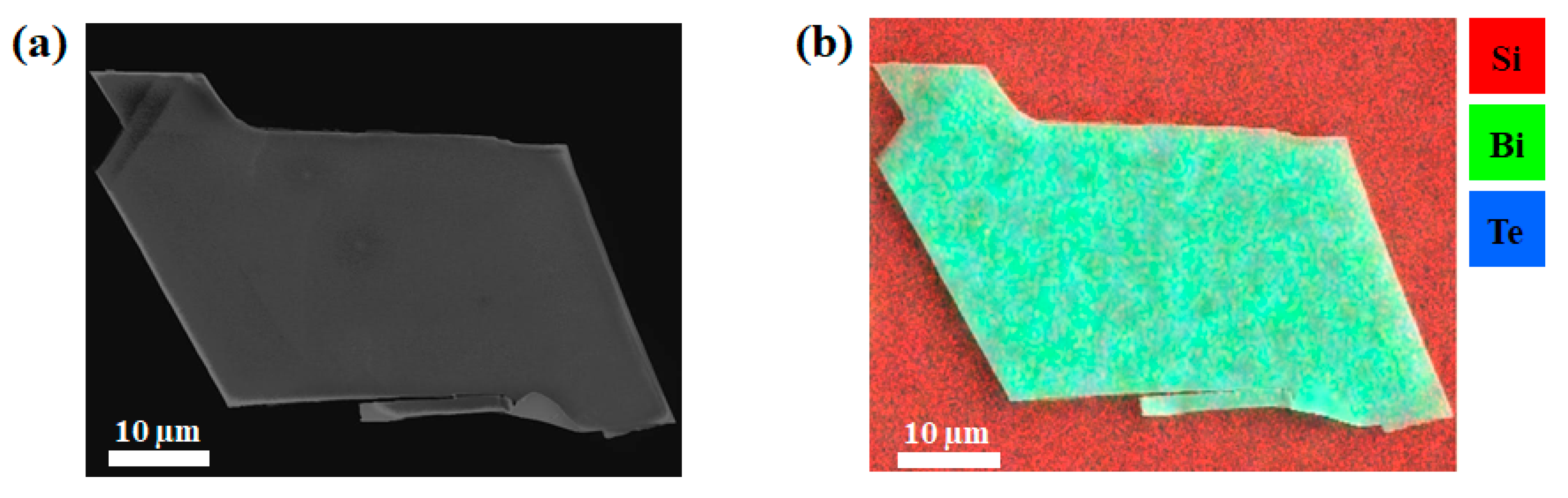
2.2. Sample Preparation and Characterization

The Bi2Te3 flake with uniform surface quality was selected and milled by FIB with 30 KeV Ga+ ions inside a FEI Nova Nano SEM450 system (Hillsboro, OR, USA). The angle between the ion beam and the electron beam is 52°. After adding the gas-phase Pt, metallic nanostructures were deposited by scanning a 15 KeV electron beam on the selected area. The surface morphology was determined by scanning electron microscope (SEM), and the elementary composition was confirmed by energy-dispersive X-ray spectroscopy (EDX) in the same chamber.

2.3. Cathodoluminescence

The light emission was characterized by cathodoluminescence (CL) in the same system. Since the signal was excited by an electron beam, the beam spot size can be as low as 5 nm. During the CL process, an Al parabolic mirror was inserted above the sample. As indicated in Figure 2a, the focused electron beam passed through a hole on the parabolic mirror and interacted with the sample. The emitted light was collected by the mirror and transmitted by a parallel waveguide to the monochromator. The CL panchromatic images were taken by a photomultiplier tube (PMT) with a functional wavelength from 300 to 900 nm. The wavelength resolved CL spectra were acquired by a CCD camera with a band-pass from 250 to 1000 nm.

2.4. Numerical Simulation

Finally, the electric field distribution at typical wavelengths was simulated by the finite element method using the COMSOL Multiphysics software (version 5.3, COMSOL INC., Burlington, NJ, USA). As indicated in Figure 2b, 2D axisymmetric models were exploited with the rotational axis on the left side. The model used a linear polarized light source with a scattering boundary condition and perfectly matched layers (PMLs). The complex dielectric constants of materials were adapted for the simulation [4,20]. Typical structural parameters were obtained from the experiment, as listed in Table 1.

3. Results and Discussion

The SEM image of a clean and flat Bi2Te3 flake is presented in Figure 3a. Directly measured in the SEM system, the average thickness of the flake is 190 nm. The EDX mapping of the flake is indicated in Figure 3b. Though the Bi2Te3 flake has a random shape, the distribution of chemical composition is uniform on the sample, making it a good candidate for further processes. Clear peaks of Bi and Te can be observed in the EDX spectrum, as presented in Figure 4a. The quantified EDX result indicates that the ratio of atomic percentage between Bi and Te is 0.679. As shown in Figure 4b, the blue curve corresponds to the CL spectrum excited at the center of the Bi2Te3 flake, while the green curve was excited from a spot on the bare substrate far away from the Bi2Te3 flake. Although peak positions are observed at 510 nm for both curves, the CL intensity on the Bi2Te3 flake is two times stronger than the substrate. We attribute this effect to the plasmonic enhancement for the semiconductor substrate [21]. Incident electrons first strike the Bi2Te3 flake and generate surface plasmon waves, then secondary electrons will also interact with the Bi2Te3 flake when they escape from the surface. Therefore, the surface plasmonic field on the Bi2Te3 flake will improve the absorption efficiency of the incident beam. Meanwhile, the enhanced electric field across the interface increases the emission efficiency.
Bullseye nanoemitters are fabricated on the same flake. As shown in Figure 5a, the SEM image indicates that a Bi2Te3 bullseye nanostructure with an 800 nm central disk diameter, a 250 nm ring width, and a 125 nm groove width has been made. Although all patterns are milled to reach the Si substrate, no contamination is found inside the gap or on edges, as indicated by the EDX mapping in Figure 5b. The panchromatic CL image of the same bullseye nanostructure is presented in Figure 5c. The CL intensity is obviously higher on the bullseye pattern. The integrated intensity at the geometric center of the Bi2Te3 bullseye nanostructure is about 1.67 times higher than the integrated intensity on the flake with no pattern. On the central disk, the edge is brighter than the center, indicating that the edge plasmonic modes are dominant. Since electrons are preferred to accumulate at the boundary, the edge behaves similar to a combination of point sources [12]. Surface waves propagate along both positive and negative radial directions [22]. Therefore, the plasmonic resonance increases towards the center and decays outside the pattern. Normalized CL spectra from four locations on the central disk are shown in Figure 5d. These spectra were normalized based on the CL signal excited from the center of the Bi2Te3 flake. The color of curves corresponds to the color of excitation positions showing as dots in Figure 5a. From the center to the edge, fitted values of the full width at half maximum (FWHM) are 352.69, 236.83, 144.18, and 120.95, respectively. Due to the intense confinement of oscillating charges, stronger plasmonic modes arise at the edge. Therefore, CL emission peaks become wider towards the edge.
In order to further improve the focusing ability of the Bi2Te3 bullseye nanoemitter, a cylindrical Pt nanostructure is deposited on the central disk. The SEM image and the EDX mapping have been depicted in Figure 6a,b. The Pt nanostructure has a 400 nm diameter and a 100 nm height. Moreover, the panchromatic CL image after the Pt deposition is presented in Figure 6c. Compared with Figure 5c, the CL emission from the center of the Bi2Te3 bullseye nanoemitter has been dramatically improved. During the experiment, the incident electron beam first excites the Pt nanostructure. Then, excess electrons continue interacting with the Bi2Te3 bullseye nanostructure. The emitted light has been better converged due to the plasmonic enhancement of the Pt nanostructure. To explain the mechanism of the field enhancement, cross-section images of the simulated electric field distributions at the peak wavelength (510 nm) are presented in Figure 6d. The simulated mappings are combined with their mirror images to form the whole bullseye nanostructure. For the Bi2Te3 nanoemitter without the Pt nanostructure, enhanced electric fields are distributed above the surface of the model. Due to the focusing effect of the bullseye structure, a hotspot can be observed above the central disk. When the Pt nanostructure is involved, intense electric fields can be obtained above the Bi2Te3 grating as well, however, the localized electric field at the geometric center has been dramatically improved. The enhanced electric field on the Pt can be attributed to the coupling effect of the plasmonic emission from the Bi2Te3 bullseye nanostructure and the localized electric field on the Pt nanodisk [16].
The enhancement efficiency corresponds to the ratio of I1/I2, where I1 and I2 relate to the integrated CL intensities of the nanoemitter with and without the Pt nanostructure. Figure 7 illustrates the experimental enhancement efficiency as a function of the thickness of the Pt nanostructure. For the same Pt diameter (400 nm), the highest enhancement efficiency is expected to be found on a nanoemitter with the Pt thickness between 200 and 300 nm. The plasmonic emission of the Pt nanostructure increases with the thickness from 100 to 200 nm. On the other hand, due to the shrink of the electron interaction volume inside the sample, the coupling effect attenuates at a higher Pt thickness (>300 nm).

4. Conclusions

In this paper, we investigate the plasmonic behavior of Bi2Te3 bullseye nanoemitters, which are fabricated by FIB milling onto exfoliated Bi2Te3 nanoflakes. Due to the existence of edge plasmon modes, Bi2Te3 nanoemitters obtain an excellent focusing property. Excited by the localized electron beam, the CL spectra evolve with the excitation position on the central disk of the bullseye nanostructure. The strongest plasmonic emission can be observed on the edge of the central disk. We propose that the CL intensity at the geometric center can be further improved by adding an extra Pt nanostructure. The numerical simulation indicates that the electric-field enhancement is caused by the coupling effect of the plasmonic emission from the Bi2Te3 bullseye and the Pt nanodisk. The actual size and geometry of the nanoemitter will be optimized in the future.

Author Contributions

Conceptualization, Q.Y. and B.L.; Methodology, Q.Y.; Software, X.L.; Validation, all; Formal analysis, Q.Y. and X.L.; Investigation, Q.Y.; Resources, B.L.; Data curation, Q.Y. and B.L.; Writing—original draft preparation, Q.Y. and B.L.; Writing—review and editing, all; Visualization, X.L.; Supervision, B.L.; Project administration, Q.Y. and B.L.; Funding acquisition, B.L. All authors have read and agreed to the published version of the manuscript.

Funding

The authors acknowledge the financial support by the Advanced Talents Incubation Program of the Hebei University (8012605), the National Natural Science Foundation of China (61774053), and the Natural Science Foundation of Hebei Province of China (F2019201446).

Conflicts of Interest

The authors declare no conflict of interest.

References

  1. Zhang, H.; Liu, C.X.; Qi, X.L.; Dai, X.; Fang, Z.; Zhang, S.C. Topological insulators in Bi2Se3, Bi2Te3 and Sb2Te3 with a single Dirac cone on the surface. Nat. Phys. 2009, 5, 438–442. [Google Scholar] [CrossRef]
  2. Saleemi, M.; Toprak, M.S.; Li, S.; Johnsson, M.; Muhammed, M. Synthesis, processing, and thermoelectric properties of bulk nanostructured bismuth telluride (Bi2Te3). J. Mater. Chem. 2012, 22, 725–730. [Google Scholar] [CrossRef]
  3. Anandan, P.; Omprakash, M.; Azhagurajan, M.; Arivanandhan, M.; Babu, D.R.; Koyama, T.; Hayakawa, Y. Tailoring bismuth telluride nanostructures using a scalable sintering process and their thermoelectric properties. Cryst. Eng. Comm. 2014, 16, 7956–7962. [Google Scholar] [CrossRef]
  4. Zhao, M.; Bosman, M.; Danesh, M.; Zeng, M.; Song, P.; Darma, Y.; Rusydi, A.; Lin, H.; Qiu, C.W.; Loh, K.P. Visible surface plasmon modes in single Bi2Te3 nanoplate. Nano Lett. 2015, 15, 8331–8335. [Google Scholar] [CrossRef] [PubMed]
  5. Lu, X.; Hao, Q.; Cen, M.; Zhang, G.; Sun, J.; Mao, L.; Cao, T.; Zhou, C.; Jiang, P.; Yang, X.; et al. Observation and manipulation of visible edge plasmons in Bi2Te3 nanoplates. Nano Lett. 2018, 18, 2879–2884. [Google Scholar] [CrossRef]
  6. Zhao, M.; Zhang, J.; Gao, N.; Song, P.; Bosman, M.; Peng, B.; Sun, B.; Qiu, C.W.; Xu, Q.H.; Bao, Q.; et al. Actively tunable visible surface plasmons in Bi2Te3 and their energy-harvesting applications. Adv. Mater. 2016, 28, 3138–3144. [Google Scholar] [CrossRef]
  7. Lee, K.S.; El-Sayed, M.A. Gold and silver nanoparticles in sensing and imaging: Sensitivity of plasmon response to size, shape and metal composition. J. Phys. Chem. B 2006, 110, 19220–19225. [Google Scholar] [CrossRef]
  8. Boltasseva, A.; Atwater, H.A. Low-loss plasmonic metamaterials. Science 2011, 331, 290–291. [Google Scholar] [CrossRef]
  9. Naik, G.V.; Shalaev, V.M.; Boltasseva, A. Alternative plasmonic materials: Beyond gold and silver. Adv. Mater. 2013, 25, 3264–3294. [Google Scholar] [CrossRef]
  10. Toudert, J.; Serna, R. Interband transitions in semi-metals, semiconductors, and topological insulators: A new driving force for plasmonics and nanophotonics. Opt. Mater. Express 2017, 7, 2299–2325. [Google Scholar] [CrossRef]
  11. Yin, J.; Krishnamoorthy, H.N.; Adamo, G.; Dubrovkin, A.M.; Chong, Y.; Zheludev, N.I.; Soci, C. Plasmonics of topological insulators at optical frequencies. NPG Asia Mater. 2017, 9, e425. [Google Scholar] [CrossRef]
  12. Liu, Z.; Steele, J.M.; Srituravanich, W.; Pikus, Y.; Sun, C.; Zhang, X. Focusing surface plasmons with a plasmonic lens. Nano Lett. 2005, 5, 1726–1729. [Google Scholar] [CrossRef] [PubMed]
  13. Ma, Q.; Liu, G.; Chen, Y.; Zhao, Q.; Guo, J.; Yang, S.; Cai, W. Surface plasmon resonance and polarization change properties in centrosymmetric nanoright-triangle dimer arrays. Opt. Eng. 2018, 57, 036112. [Google Scholar] [CrossRef]
  14. Luo, Y.; Chamanzar, M.; Apuzzo, A.; Salas-Montiel, R.; Nguyen, K.N.; Blaize, S.; Adibi, A. On-chip hybrid photonic-plasmonic light concentrator for nanofocusing in an integrated silicon photonics platform. Nano Lett. 2015, 15, 849–856. [Google Scholar] [CrossRef]
  15. Mao, L.; Zang, T.; Ren, Y.; Lei, X.; Jiang, K.; Li, K.; Lu, Y.; Wang, P. Polarization-dependent transmittance of concentric rings plasmonic lens: A polarizing interference investigation. J. Opt. 2016, 18, 105006. [Google Scholar] [CrossRef]
  16. Normatov, A.; Ginzburg, P.; Berkovitch, N.; Lerman, G.M.; Yanai, A.; Levy, U.; Orenstein, M. Efficient coupling and field enhancement for the nano-scale: Plasmonic needle. Opt. Express 2010, 18, 14079–14086. [Google Scholar] [CrossRef]
  17. Garoli, D.; Zilio, P.; Gorodetski, Y.; Tantussi, F.; Angelis, F.D. Beaming of helical light from plasmonic vortices via adiabatically tapered nanotip. Nano Lett. 2016, 16, 6636–6643. [Google Scholar] [CrossRef]
  18. Friedensen, S.; Mlack, J.T.; Drndić, M. Materials analysis and focused ion beam nanofabrication of topological insulator Bi2Se3. Sci. Rep. 2017, 7, 13466. [Google Scholar] [CrossRef] [Green Version]
  19. Bando, H.; Koizumi, K.; Oikawa, Y.; Daikohara, K.; Kulbachinskii, V.A.; Ozaki, H. The time-dependent process of oxidation of the surface of Bi2Te3 studied by x-ray photoelectron spectroscopy. J. Phys. Condens. Matter 2000, 12, 5607–5616. [Google Scholar] [CrossRef]
  20. Palik, E.D. Handbook of Optical Constants of Solids I.; Academic Press Inc.: Orlando, FL, USA, 1985; pp. 290–357. [Google Scholar]
  21. Tateishi, K.; Funato, M.; Kawakami, Y.; Okamoto, K.; Tamada, K. Highly enhanced green emission from InGaN quantum wells due to surface plasmon resonance on aluminum films. Appl. Phys. Lett. 2015, 106, 121112. [Google Scholar] [CrossRef]
  22. Yao, W.; Liu, S.; Liao, H.; Li, Z.; Sun, C.; Chen, J.; Gong, Q. Efficient directional excitation of surface plasmons by a single-element nanoantenna. Nano Lett. 2015, 15, 3115–3121. [Google Scholar] [CrossRef] [PubMed]
Figure 1. Image of Bi2Te3 flakes after exfoliation. The inset is showing the Bi2Te3 crystal before exfoliation.
Materials 13 01531 g001
Figure 2. Schematics of (a) the cathodoluminescence (CL) setup and (b) basic models for the numerical simulation.
Materials 13 01531 g002
Figure 3. (a) SEM image of a Bi2Te3 flake; (b) EDX mapping of the same Bi2Te3 flake.
Materials 13 01531 g003
Figure 4. (a) EDX spectrum of the same Bi2Te3 flake; (b) CL spectra collected from the Bi2Te3 flake and the substrate.
Materials 13 01531 g004
Figure 5. (a) SEM image of a bullseye nanostructure on the Bi2Te3 flake; (b,c) are the EDX mapping and the CL panchromatic image of the same bullseye nanostructure; (d) normalized CL spectra excited at four positions on the central disk.
Materials 13 01531 g005
Figure 6. (a) SEM image of the Bi2Te3 nanoemitter with a Pt nanostructure; (b,c) are the EDX mapping and the CL panchromatic image of the same nanoemitter; (d) simulated cross-section electric field distributions of the Bi2Te3 nanoemitter with and without the Pt nanostructure at 510 nm.
Materials 13 01531 g006
Figure 7. Enhancement efficiencies for nanoemitters with different Pt thickness.
Materials 13 01531 g007
Table 1. Typical structural parameters used in the simulation.
ParameterDescriptionValue
T1Thickness of Bi2Te3 flakes190 nm
T2Thickness of the Pt structure100 nm
R1Radius of the central disk400 nm
R2Radius of the Pt structure200 nm
W1Width of grooves125 nm
W2Width of rings250 nm

