Fabrication of SiC Sealing Cavity Structure for All-SiC Piezoresistive Pressure Sensor Applications


Abstract
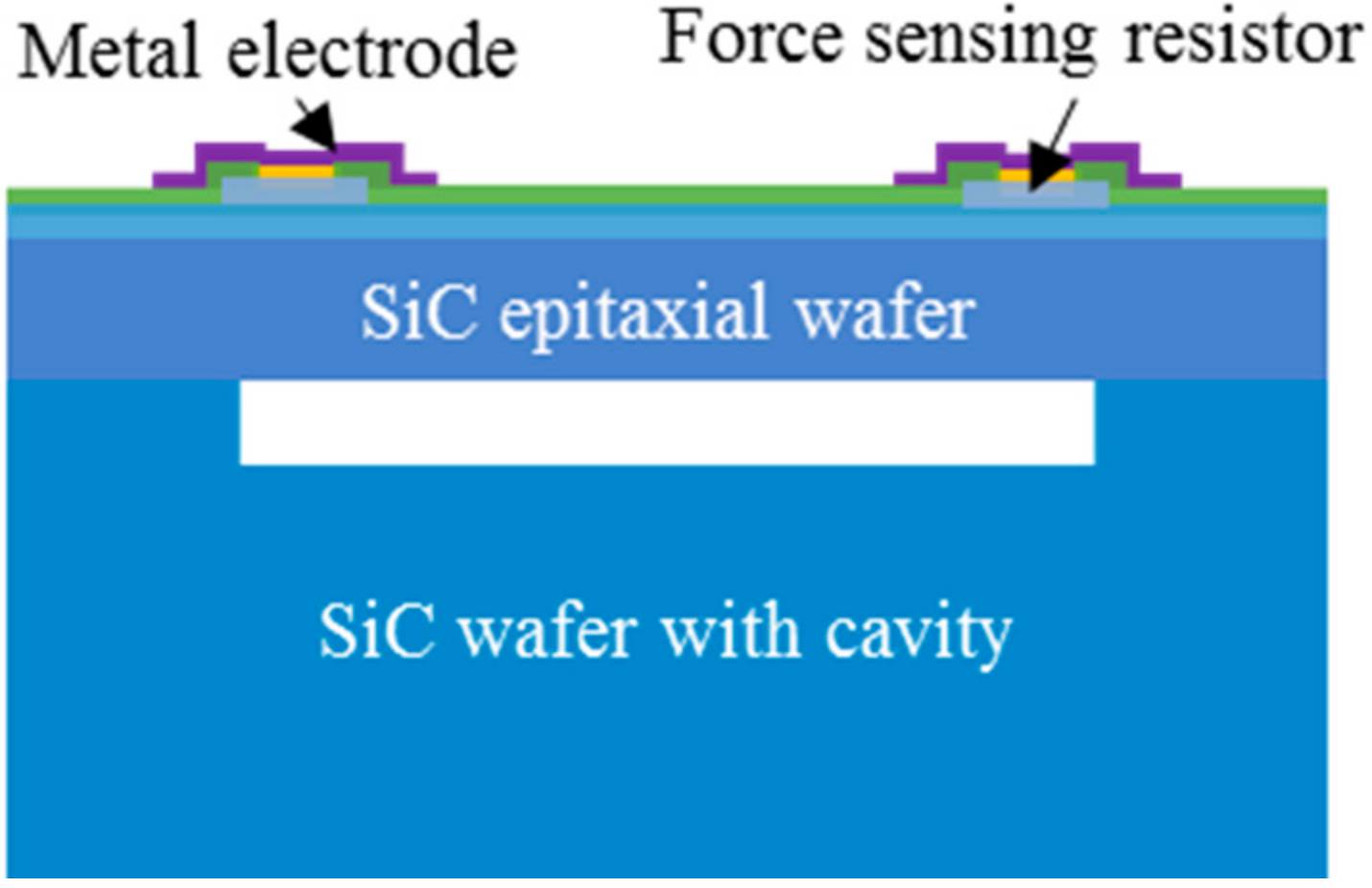
:1. Introduction
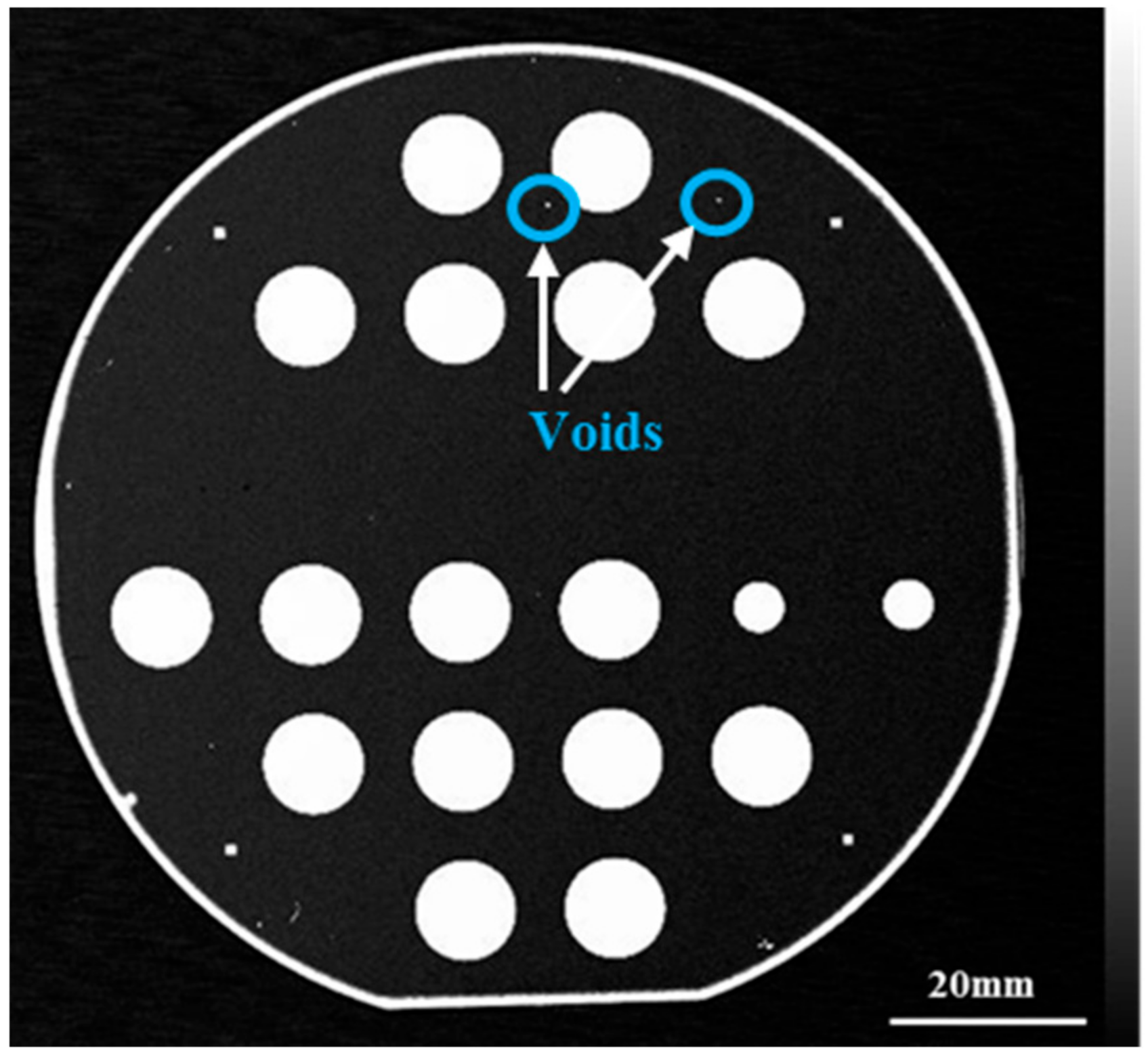
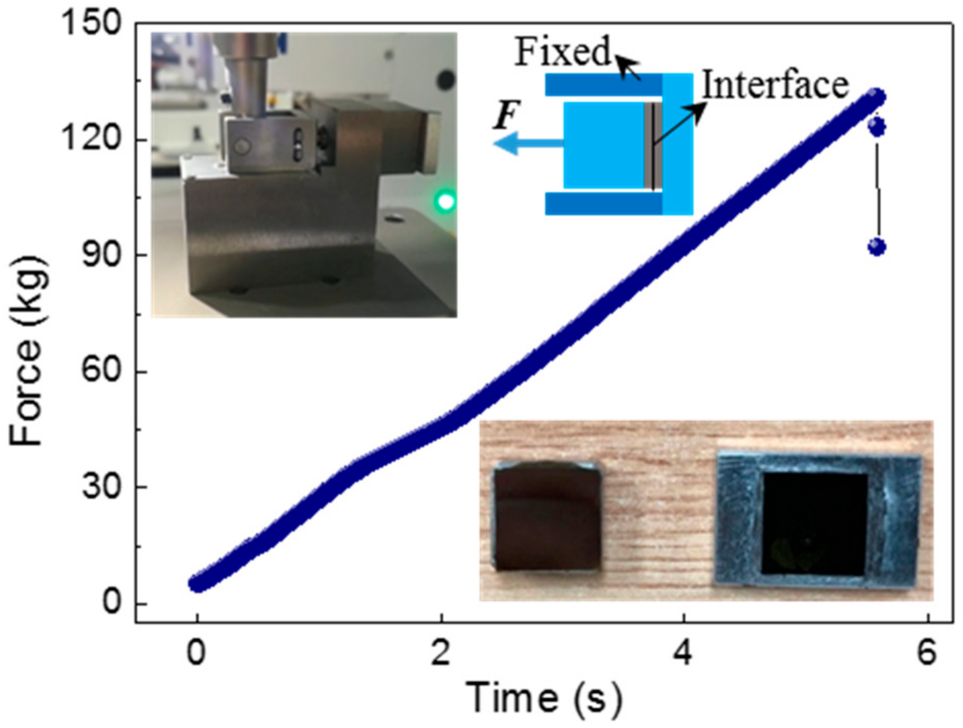
2. Experimental Procedures
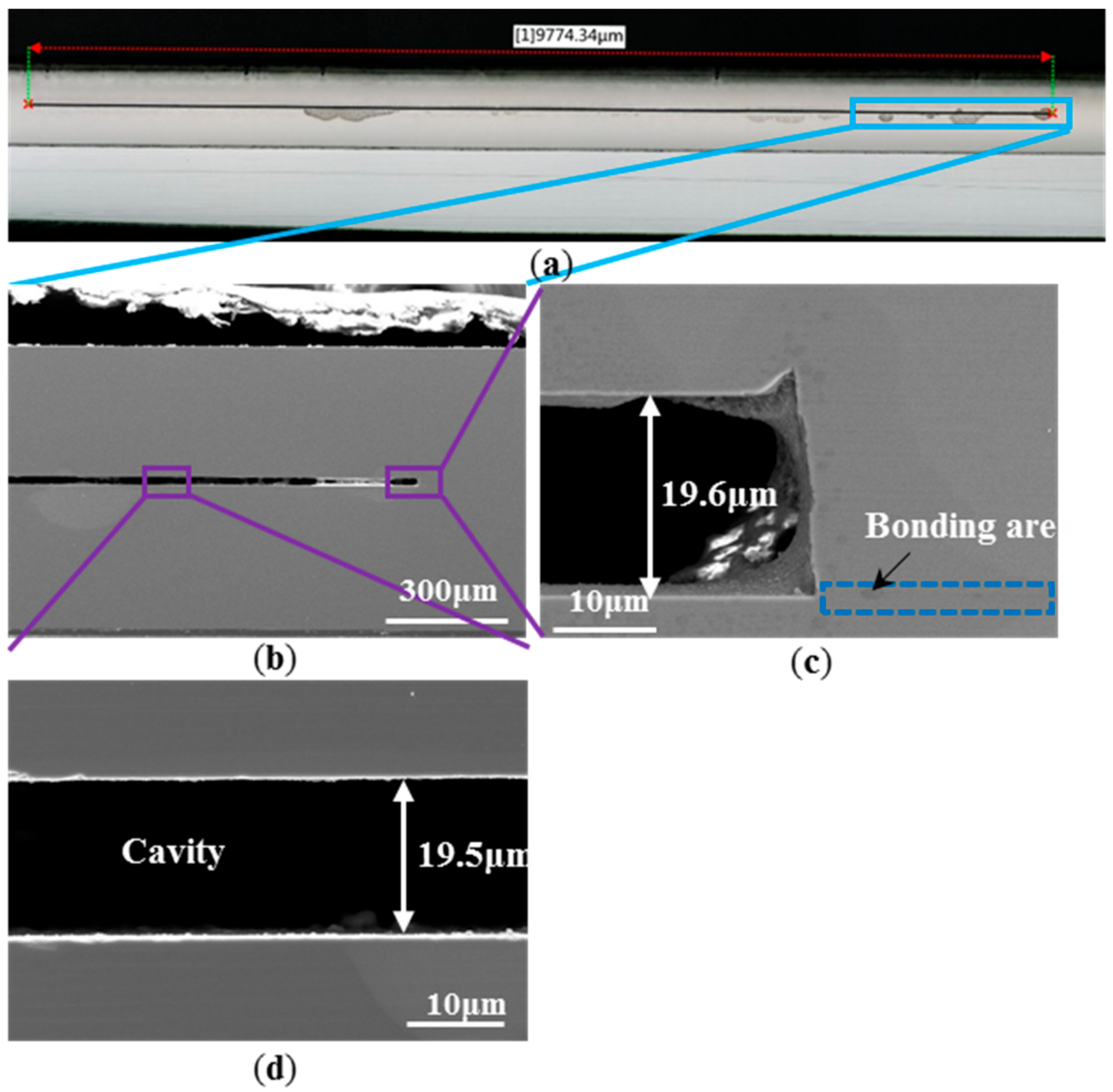
3. Results and Discussion
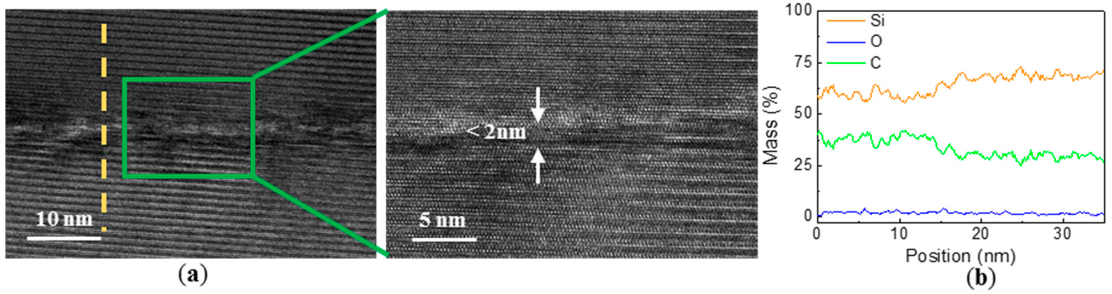
3.1. Characterization of Bonding Interface before Annealing
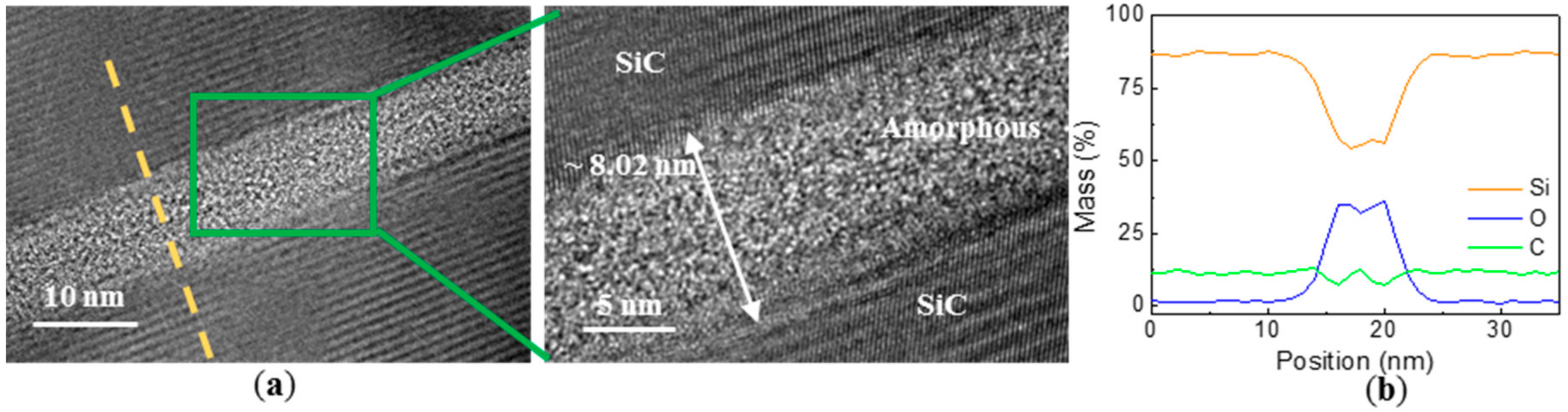
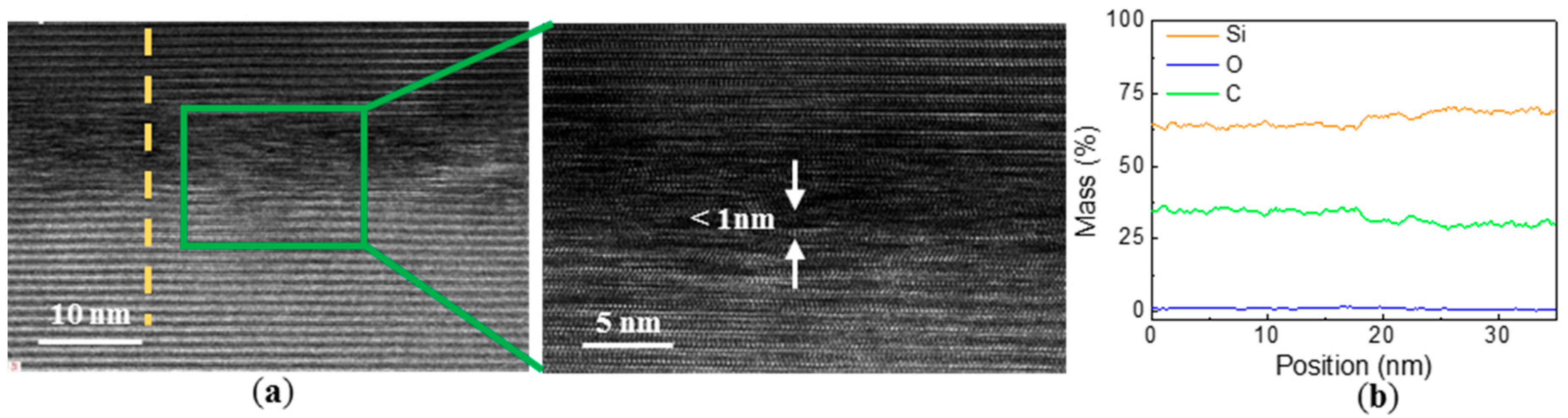
3.2. Characterization of Bonding Interface after Annealing
4. Conclusions
Author Contributions
Funding
Data Availability Statement
Conflicts of Interest
References
- Seo, Y.; Kim, D.; Hall, N.A. On-diaphragm thermistor for high-temperature dynamic pressure sensors. IEEE Sens. J. 2020, 20, 2287–2293. [Google Scholar] [CrossRef]
- Yang, C.; Maimaitiyiming, X.; Mi, H. High temperature sensitivity pressure sensors based on filter paper as a mold. J. Electrochem. Soc. 2019, 166, B1286–B1292. [Google Scholar] [CrossRef]
- Zhang, J.; Lei, Y.; Chen, Y.; Chuan, H. 3D printing of all-glass fiber-optic pressure sensor for high temperature applications. IEEE Sens. J. 2019, 19, 11242–11246. [Google Scholar] [CrossRef] [PubMed]
- Phan, H.P.; Dao, D.V.; Nakamura, K.; Dimitrijev, S.; Nguyen, N.-T. The piezoresistive effect of SiC for MEMS sensors at high temperatures: A review. J. Microelectromech. Syst. 2015, 24, 1663–1677. [Google Scholar] [CrossRef] [Green Version]
- Jiang, X.; Kim, K.; Zhang, S.; Johnson, J.; Salazar, G. High-temperature piezoelectric sensing. Sensors 2013, 14, 144–169. [Google Scholar] [CrossRef] [Green Version]
- Wijesundara, M.B.J.; Azevedo, R.G. Silicon Carbide Microsystems for Harsh Environments; Springer: New York, NY, USA, 2011; pp. 129–132. [Google Scholar]
- Fahrner, W.R.; Job, R.; Werner, M. Sensors and smart electronics in harsh environment applications. Microsyst. Technol. 2001, 7, 138–144. [Google Scholar] [CrossRef]
- Giuliani, A.; Drera, L.; Arancio, D.; Mukhopadhyay, B.; Ngo, H.D. SOI-based, high reliable pressure sensor with floating concept for high temperature applications. Procedia Eng. 2014, 87, 720–723. [Google Scholar] [CrossRef] [Green Version]
- Li, C.; Zhao, L.; José, L.; Cordovilla, F.O.; Yin, Z. Characterization and analysis of a novel structural SOI piezoresistive pressure sensor with high sensitivity and linearity. Microsyst. Technol. 2020, 26, 2955–2960. [Google Scholar] [CrossRef]
- Jiang, L.; Cheung, R. A review of silicon carbide development in MEMS applications. Int. J. Comput. Mater. Sci. Surf. Eng. 2009, 2, 227–242. [Google Scholar] [CrossRef] [Green Version]
- Nguyen, T.-K.; Phan, H.P.; Han, J.; Dinh, T.; Foisal, A.R.M.; Dimitrijev, S.; Zhu, Y.; Nguyen, N.-T.; Dao, D.V. Highly sensitive p-Type 4H-SiC van der Pauw sensor. RSC Adv. 2018, 8, 3009–3013. [Google Scholar] [CrossRef] [Green Version]
- Okojie, R.S.; Howard, R.T.; Richards, R.D. Stable 600 °C silicon carbide MEMS pressure transducers. Proc SPIE Int. Soc. Opt. Eng. 2007, 6555, 6550V. [Google Scholar]
- Okojie, R.S.; Lukco, D.; Nguyen, V.; Savrun, E. 4H-SiC piezoresistive pressure sensors at 800 ℃ with observed sensitivity recovery. IEEE Electron Device Lett. 2015, 36, 174–176. [Google Scholar] [CrossRef]
- Jin, S.; Rajgopal, S.; Mehregany, M. Characterization of poly-sic pressure sensors for high temperature and high pressure applications. Mater. Sci. Forum 2012, 717–720, 1211–1214. [Google Scholar] [CrossRef]
- Tang, F.; Ma, X.; Wang, X. A study on the deep etching and ohmic contact process of 6H-SiC high-temperature pressure sensor. Proc. Inst. Mech. Eng. Part J. Nanoeng. Nanosyst. 2013, 229, 23–27. [Google Scholar] [CrossRef]
- Okojie, R.S.; Ned, A.A.; Kurtz, A.D. Operation of α(6H)-SiC pressure sensor at 500 °C. Sens. Actuators A Phys. 1998, 66, 200–204. [Google Scholar] [CrossRef]
- Akiyama, T.; Briand, D.; Rooij, N.F.D. Piezoresistive n-type 4H-SiC pressure sensor with membrane formed by mechanical milling. In Proceedings of the 2011 IEEE Sensors, Limerick, Ireland, 28–31 October 2011; pp. 222–225. [Google Scholar]
- Nguyen, T.K.; Phan, H.P.; Dinh, T.; Dowling, K.M.; Foisal, A.R.M.; Senesky, D.G.; Nguyen, N.; Dao, D.V. Highly sensitive 4H-SiC pressure sensor at cryogenic and elevated temperatures. Mater. Des. 2018, 156, 441–445. [Google Scholar] [CrossRef]
- Wieczorek, G.; Schellin, B.; Obermeier, E. SiC Based Pressure Sensor for High-Temperature Environments. In Proceedings of the 2007 IEEE Sensors, Atlanta, GA, USA, 28–31 October 2007; pp. 748–751. [Google Scholar]
- Pan, G.; Zhou, Y.; Luo, G.; Shi, X.; Zou, C.; Gong, H. Chemical mechanical polishing (CMP) of on-axis Si-face 6H-SiC wafer for obtaining atomically flat defect-free surface. J. Mater. Sci. Mater. Electron. 2013, 24, 5040–5047. [Google Scholar] [CrossRef]
- Shi, X.; Pan, G.; Zhou, Y.; Gu, Z.; Gong, H.; Zou, C. Characterization of colloidal silica abrasives with different sizes and their chemical–mechanical polishing performance on 4H-SiC (0001). Appl. Surf. Sci. 2014, 307, 414–427. [Google Scholar] [CrossRef]
- Aida, H.; Doi, T.; Takeda, H.; Katakura, H.; Uneda, M. Ultraprecision CMP for sapphire, gan, and SiC for advanced optoelectronics materials. Curr. Appl. Phys. 2012, 12, S41–S46. [Google Scholar] [CrossRef]
- Chen, X.; Xu, X.; Li, J.; Jiang, S.; Ning, L.; Wang, Y.; Ma, D.; Hu, X.; Jiang, M. Surface polishing of 6H-SiC substrates. J. Mater. Sci. Technol. 2007, 23, 430–432. [Google Scholar]
- Yushin, G.N.; Kvit, A.V.; Sitar, Z. Transmission electron microscopy studies of the bonded SiC-SiC interface. J. Mater. Sci. 2005, 40, 4369–4371. [Google Scholar] [CrossRef]
- Mu, F.; Uomoto, M.; Shimatsu, T.; Wang, Y.; Iguchi, K.; Nakazawa, H.; Takahashi, Y.; Higurashi, E.; Suga, T. De-bondable SiCSiC wafer bonding via an intermediate Ni nano-film. Appl. Surf. Sci. 2019, 465, 591–595. [Google Scholar] [CrossRef]
- Chung, G.S.; Maboudian, R. Bonding characteristics of 3C-SiC wafers with hydrofluoric acid for high-temperature MEMS applications. Sens. Actuators A Phys. 2005, 119, 599–604. [Google Scholar] [CrossRef]
- Veggel, A.A.V.; Ende, D.V.D.; Bogenstahl, J.; Rowan, S.; Cunningham, W.; Gubbels, G.H.M.; Nijmeijer, H. Hydroxide catalysis bonding of silicon carbide. J. Eur. Ceram. Soc. 2008, 28, 303–310. [Google Scholar] [CrossRef] [Green Version]
- Zhao, L.; Shang, H.; Wang, D.; Liu, Y.; Xue, M.; Yu, J.; Wang, W. Surface cleaning process for plasma-etched SiC wafer. Appl. Phys. A Mater. Sci. Process 2020, 126, 617. [Google Scholar] [CrossRef]
- Mu, F.; Iguchi, K.; Nakazawa, H.; Takahashi, Y.; Fujino, M.; Suga, T. Direct Wafer Bonding of SiC-SiC by SAB for Monolithic Integration of SiC MEMS and Electronics. ECS J. Solid State Sci. Technol. 2016, 5, 451–456. [Google Scholar] [CrossRef]
- Mu, F.; Fujino, M.; Suga, T.; Takahashi, Y.; Nakazawa, H.; Iguchi, K. A comparison study: Direct wafer bonding of SiC–SiC by standard surface-activated bonding and modified surface-activated bonding with Si-containing Ar ion beam. Appl. Phys. Express 2016, 9, 081302. [Google Scholar] [CrossRef]
- Mills, D.A.; Alexander, D.; Subhash, G.; Sheplak, M. Development of a sapphire optical pressure sensor for high-temperature applications. Int. Soc. Opt. Photonics 2014, 9113, 91130H. [Google Scholar]

Publisher’s Note: MDPI stays neutral with regard to jurisdictional claims in published maps and institutional affiliations. |
© 2020 by the authors. Licensee MDPI, Basel, Switzerland. This article is an open access article distributed under the terms and conditions of the Creative Commons Attribution (CC BY) license (http://creativecommons.org/licenses/by/4.0/).
Share and Cite
Zhao, L.; Shang, H.; Wang, D.; Liu, Y.; Tian, B.; Wang, W. Fabrication of SiC Sealing Cavity Structure for All-SiC Piezoresistive Pressure Sensor Applications. Materials 2021, 14, 128. https://doi.org/10.3390/ma14010128
Zhao L, Shang H, Wang D, Liu Y, Tian B, Wang W. Fabrication of SiC Sealing Cavity Structure for All-SiC Piezoresistive Pressure Sensor Applications. Materials. 2021; 14(1):128. https://doi.org/10.3390/ma14010128
Chicago/Turabian StyleZhao, Lihuan, Haiping Shang, Dahai Wang, Yang Liu, Baohua Tian, and Weibing Wang. 2021. "Fabrication of SiC Sealing Cavity Structure for All-SiC Piezoresistive Pressure Sensor Applications" Materials 14, no. 1: 128. https://doi.org/10.3390/ma14010128