
Surface Stoichiometry and Depth Profile of Tix-CuyNz Thin Films Deposited by Magnetron Sputtering

 ,
, 
Abstract
:1. Introduction
2. Materials And Methods
2.1. Ti-CuN Film Synthesis by Combination of DCMS and Hipims
2.2. Ar Etching and Thickness Measurement
2.3. Film Characterization
3. Results And Discussion
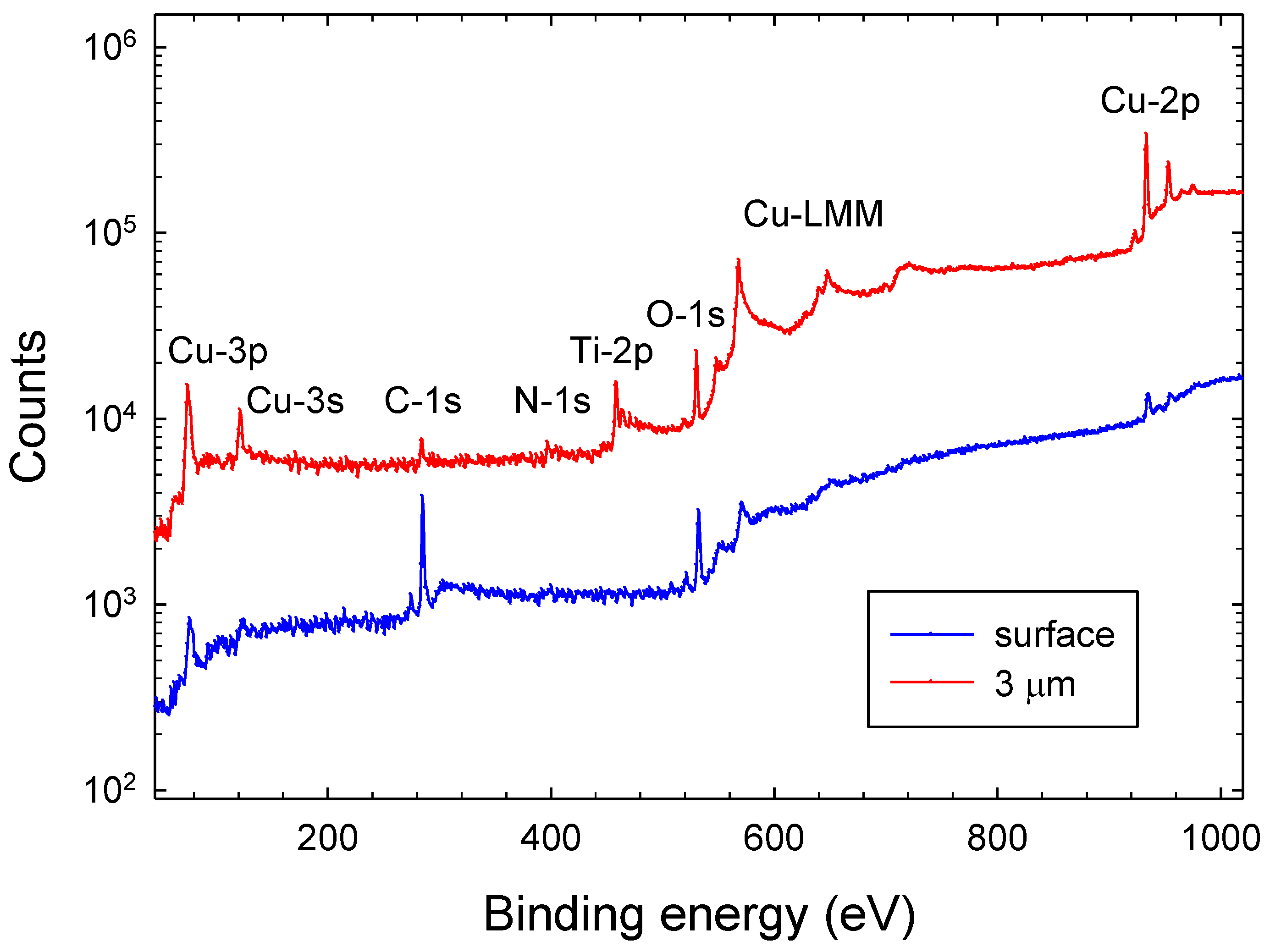
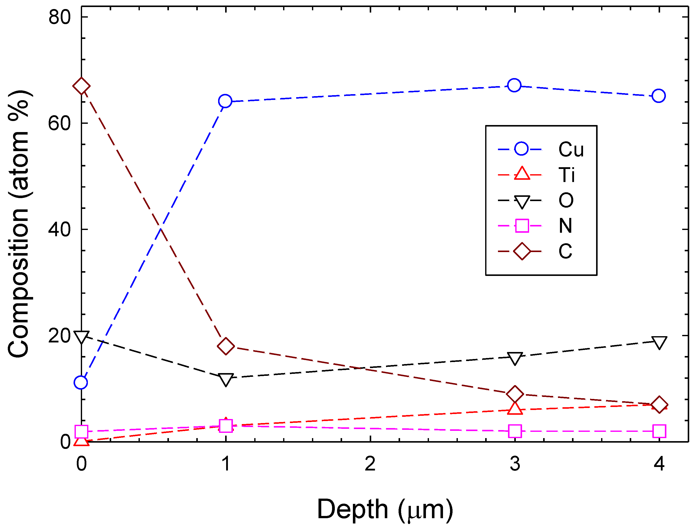
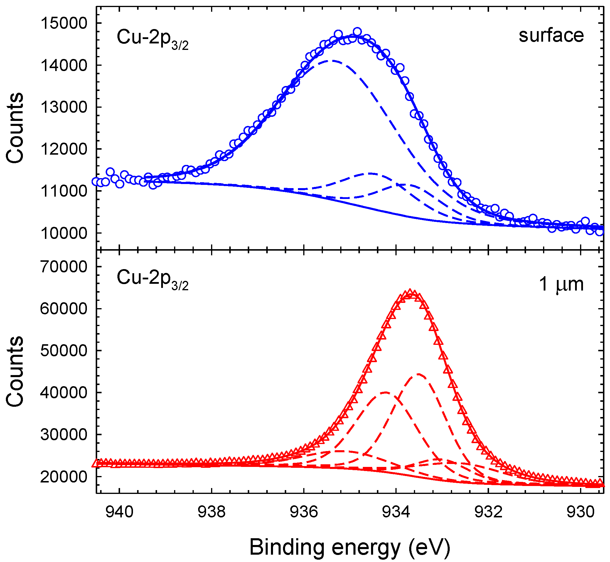
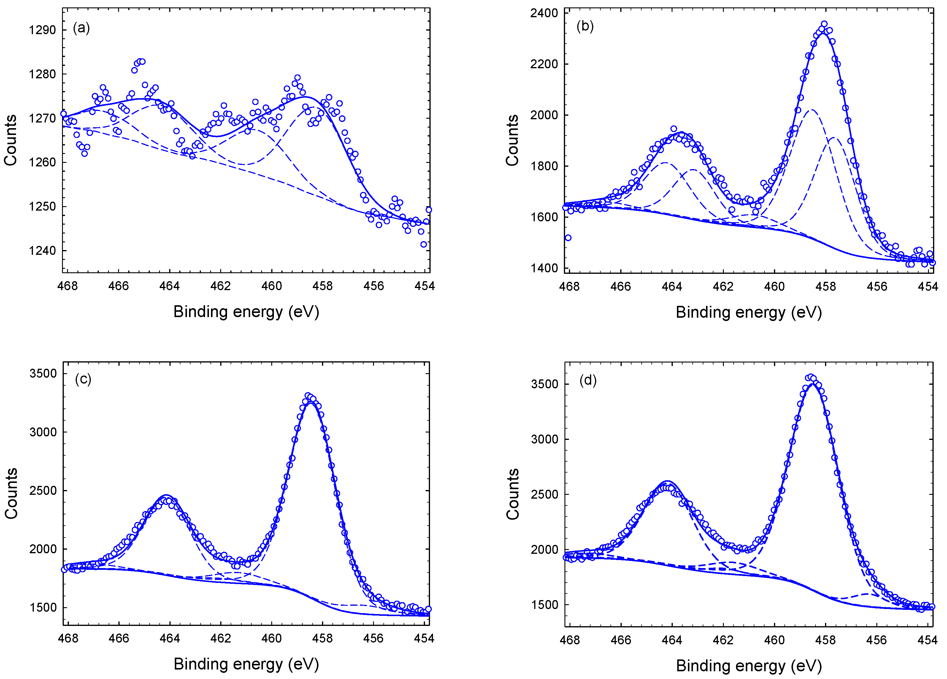
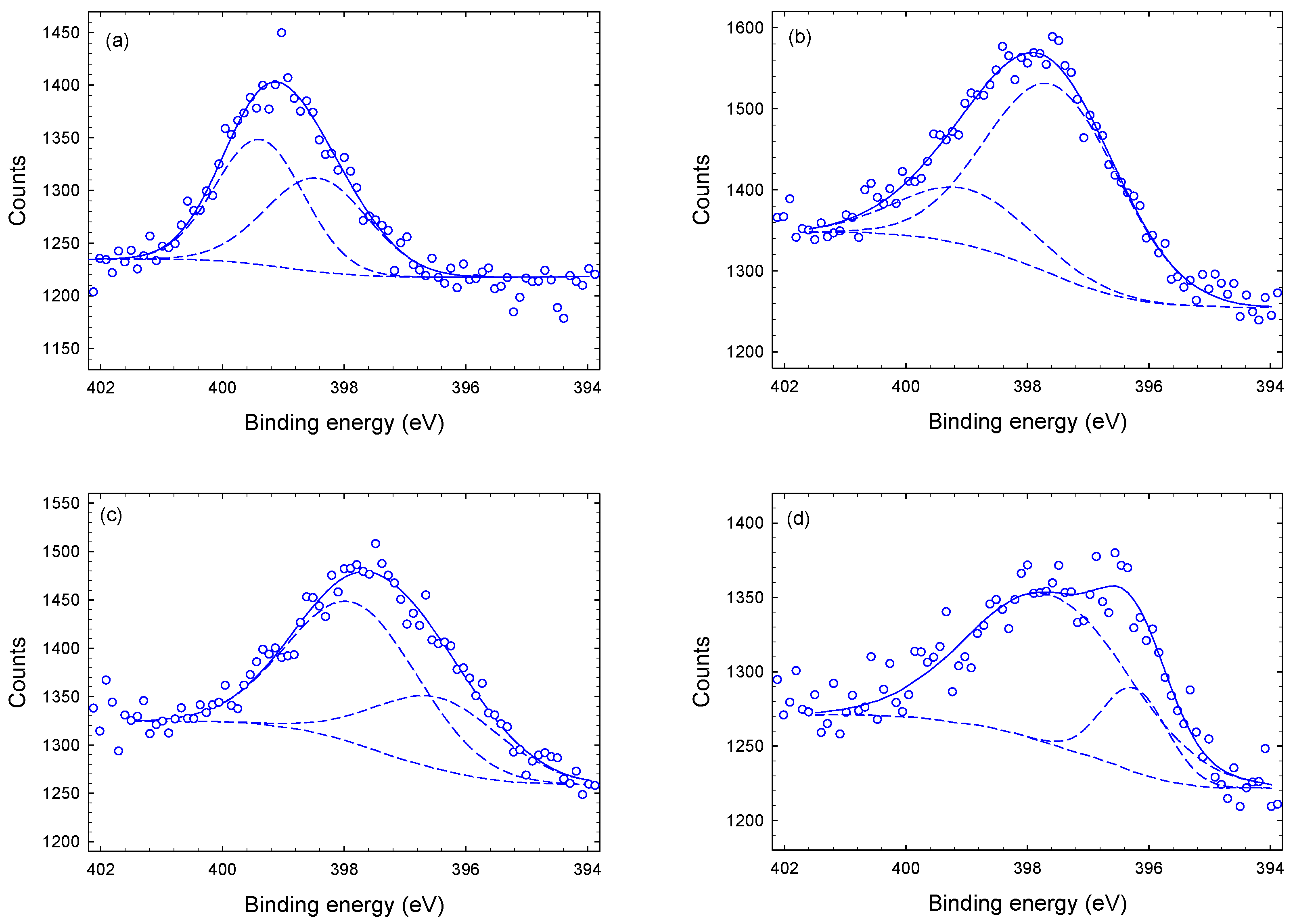
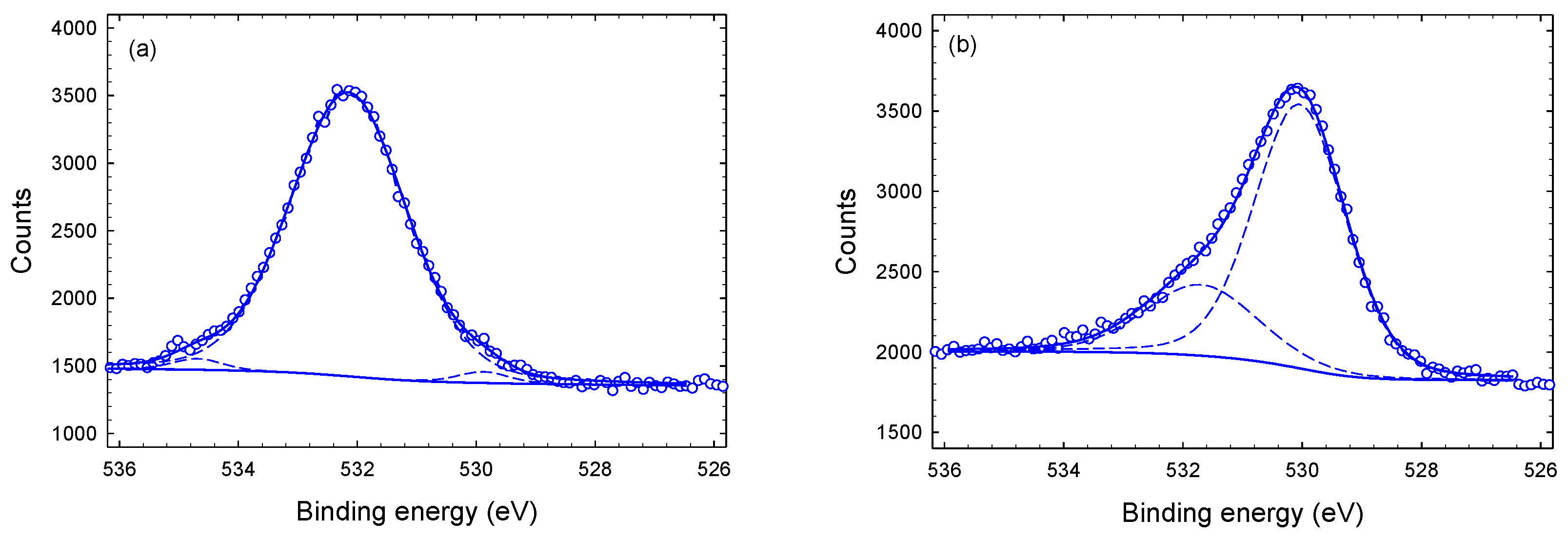
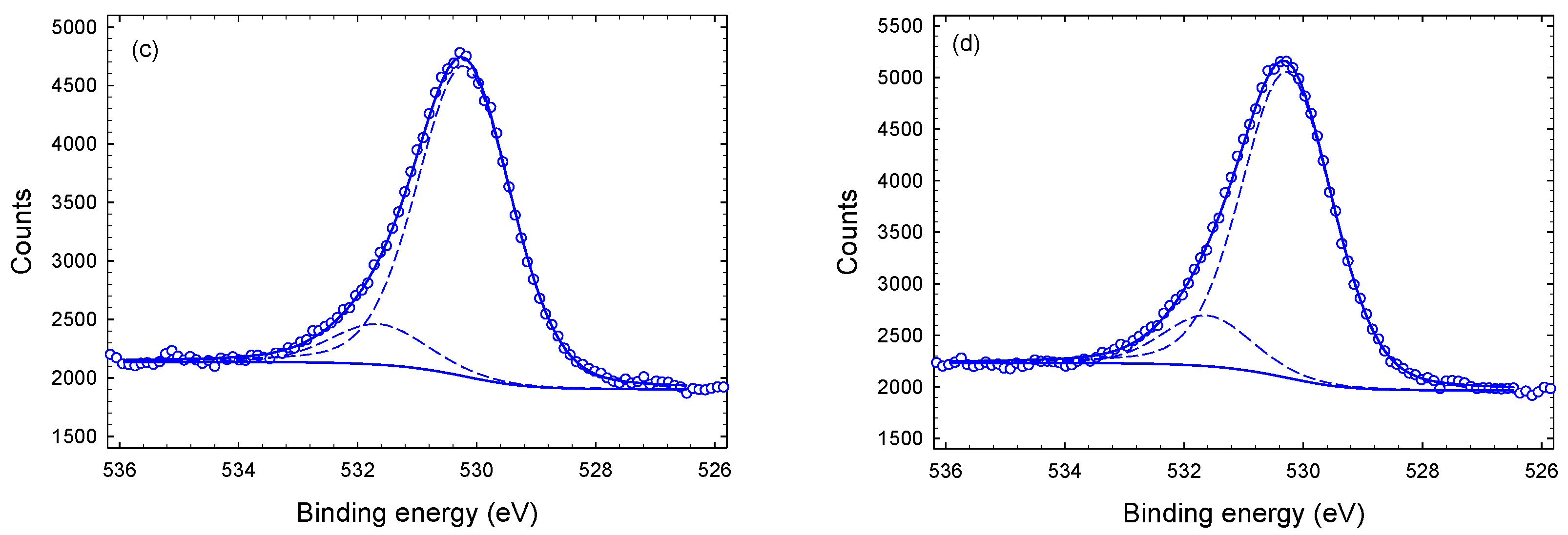
3.1. Chemical Composition and Bond Structure
3.2. GIXD of Ti-CuN Film
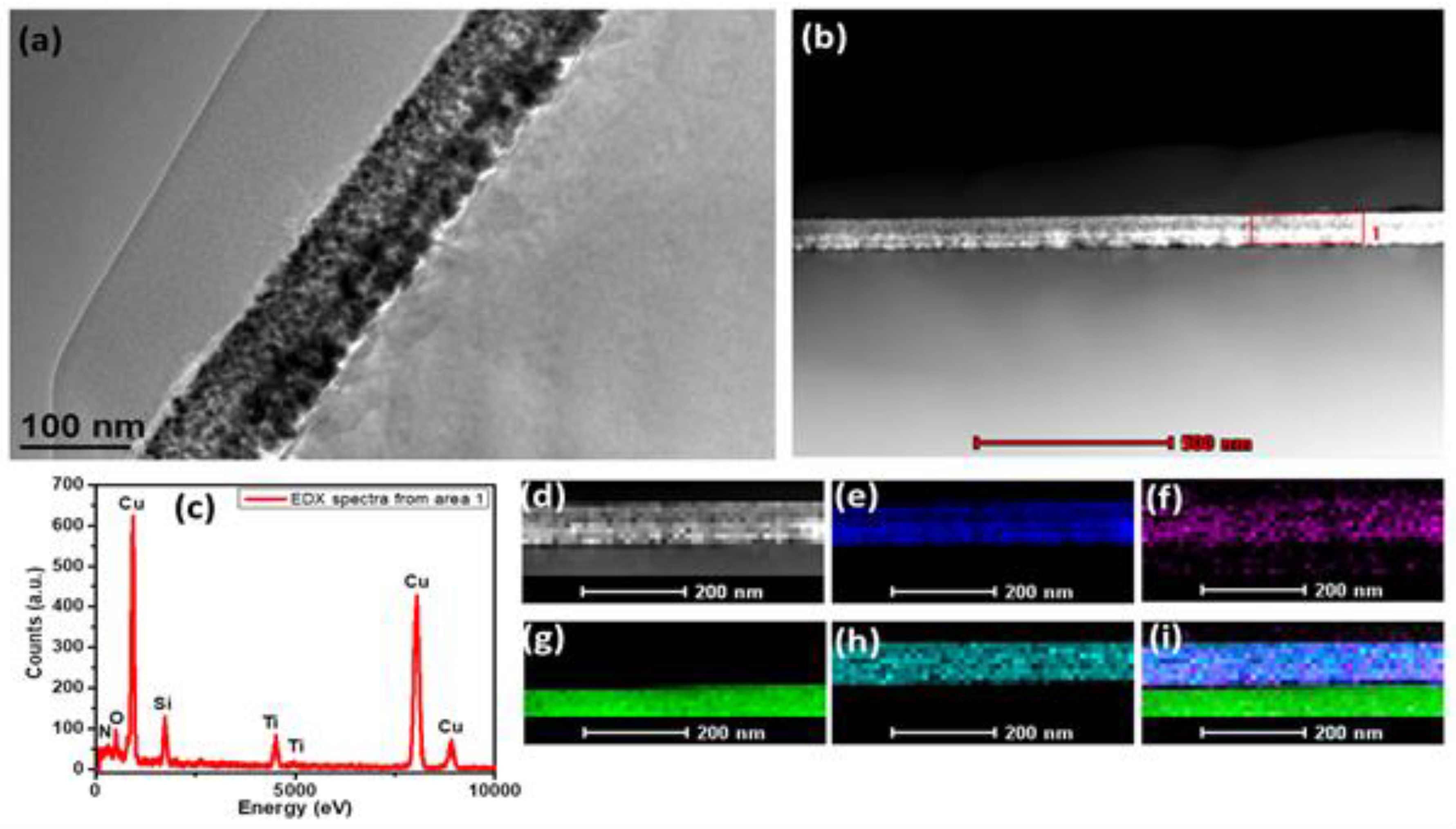
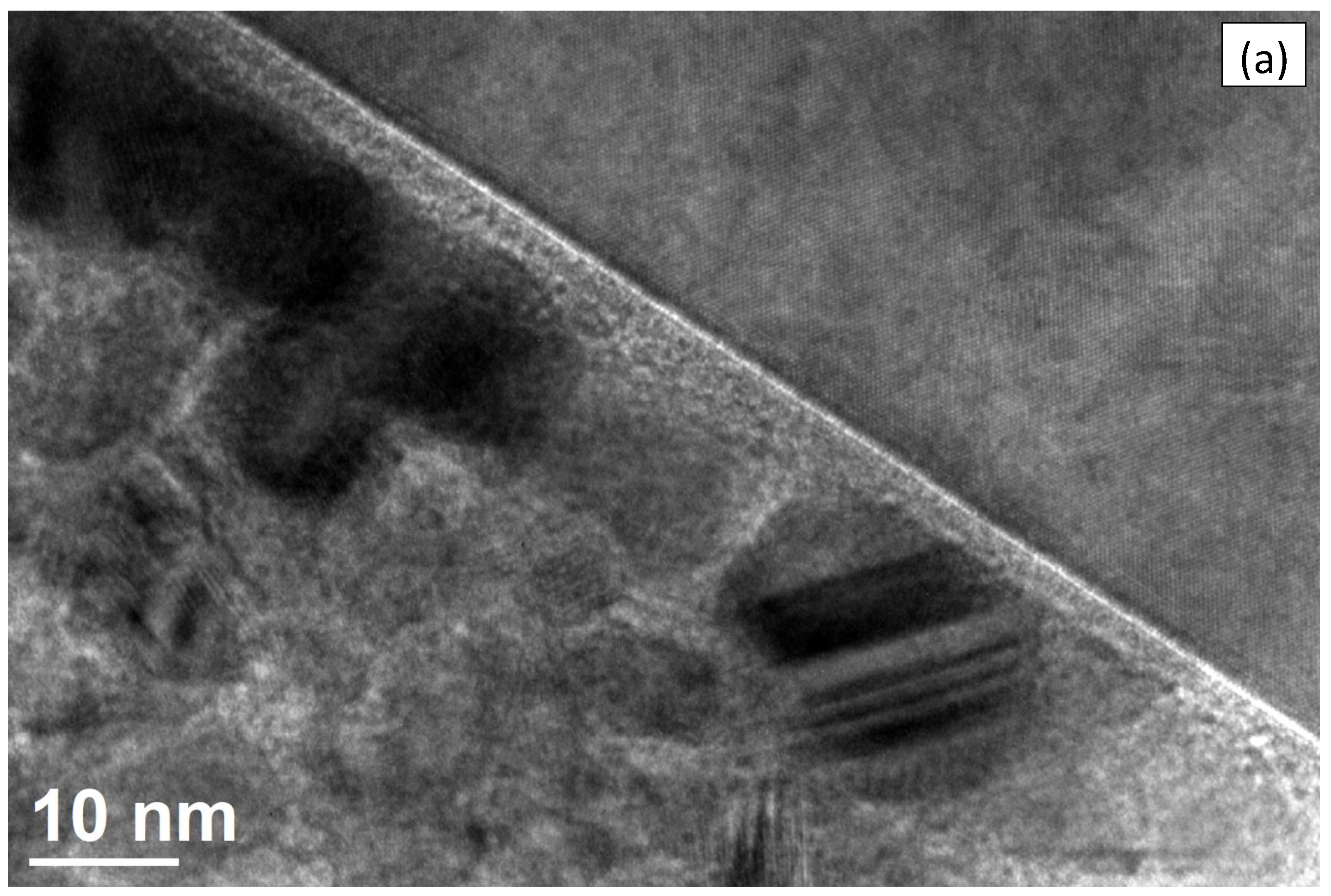
3.3. TEM and EDX of Ti-CuN Film
4. Conclusions
Author Contributions
Funding
Institutional Review Board Statement
Informed Consent Statement
Data Availability Statement
Acknowledgments
Conflicts of Interest
Abbreviations
| DCMS | Direct current magnetron sputtering |
| EDX | Energy dispersive X-ray spectroscopy |
| GIXD | Grazing incidence X-ray diffraction |
| HAADF | High-angle annular dark field |
| HiPIMS | High power impulse magnetron sputtering |
| HRTEM | High resolution TEM |
| SAED | Selected area electron diffraction |
| TEM | Transmission electron microscopy |
| XPS | X-ray photoelectron spectroscopy |
| XRD | X-ray diffraction |
References
- Fernandez, I.; Martin-Gonzalez, M.S.; Gonzalez-Arrabal, R.; lvarez, R.A.; Briones, F.; Costa-Kramer, J.L. Nitrided FeB amorphous thin films for magneto mechanical systems. J. Magn. Magn. Mater. 2008, 320, 68. [Google Scholar] [CrossRef]
- Coey, J.M.D.; Smith, P.A.I. Magnetic nitrides. J. Magn. Magn. Mater. 1999, 200, 405. [Google Scholar] [CrossRef]
- Schaaf, P.; Illgner, C.; Niederdrenk, M.; Lieb, K.P. Characterization of laser-nitrided iron and sputtered iron nitride films. Hyperfine Interact. 1995, 95, 199. [Google Scholar] [CrossRef]
- Wang, J.; Zhao, B.; Li, G.; Yang, K.; Yu, J.; Yang, X.; Zhan, D. Study of TiCu/TiCuN multilayer films with antibacterial activity. Mater. Technol. 2020, 35, 475. [Google Scholar] [CrossRef]
- Peng, C.; Zhao, Y.; Jin, S.; Wang, J.; Liu, R.; Liu, H.; Shi, W.; Kolawole, S.K.; Ren, L.; Yu, B.; et al. Antibacterial TiCu/TiCuN Multilayer Films with Good Corrosion Resistance Deposited by Axial Magnetic Field-Enhanced Arc Ion Plating. ACS Appl. Mater. Interfaces 2019, 11, 125. [Google Scholar] [CrossRef]
- Stranak, V.; Wulff, H.; Ksirova, P.; Zietz, C.; Drache, S.; Cada, M.; Hubicka, Z.; Bader, R.; Tichy, M.; Helm, C.A. Ionized vapor deposition of antimicrobial Ti-Cu films with controlled copper release. Thin Solid Film. 2014, 550, 389. [Google Scholar] [CrossRef]
- Asano, M.; Umeda, K.; Tasaki, A. Cu3N Thin Film for a New Light Recording Media. Jpn. J. Appl. Phys. 1990, 29, 1985. [Google Scholar] [CrossRef]
- Maruyama, T.; Morishita, T. Copper nitride thin films prepared by radio-frequency reactive sputtering. J. Appl. Phys. 1995, 78, 4104. [Google Scholar] [CrossRef] [Green Version]
- Nosaka, T.; Yoshitake, M.; Okamoto, A.; Ogawa, S.; Nakayama, Y. Thermal decomposition of copper nitride thin films and dots formation by electron beam writing. Appl. Surf. Sci. 2001, 169–170, 358–361. [Google Scholar] [CrossRef]
- Borsa, D.M. Nitride-Based Insulating and Magnetic Thin Films and Multilayers. Ph.D. Thesis, Groningen University, Groningen, The Netherlands, 2004. [Google Scholar]
- Niu, J.; Gao, W.; Dong, X.; Guan, L.; Xie, F. First principles calculations of optical properties of Cu3N and Cu4N. Adv. Mater. Res. 2010, 150–151, 1290. [Google Scholar] [CrossRef]
- Jones, A.P.; Beard, A.D.; Milledge, H.J.; Cressey, G.; Kirk, C.; DeCarli, P. New nitride minerals in carbonado diamond. In Proceedings of the 8th International Kimberlite Conference, Victoria, Extended Abstracts, Victoria, BC, Canada, 22–27 June 2003; Volume 8, ISBN 978-1-55195-422-6. [Google Scholar]
- Cristina, L.J.; Vidal, R.A.; Ferrn, J. Surface characterization of nitride structures on Cu(0 0 1) formed by implantation of N ions: An AES, XPS and LEIS study. Surf. Sci. 2008, 602, 3454–3458. [Google Scholar] [CrossRef]
- Gallardo-Vega, C.; Cruz, W.D. Study of the structure and electrical properties of the copper nitride thin films deposited by pulsed laser deposition. Appl. Surf. Sci. 2006, 252, 8001. [Google Scholar] [CrossRef]
- Pierson, J.F. Structure and properties of copper nitride films formed by reactive magnetron sputtering. Vacuum 2002, 66, 59–64. [Google Scholar] [CrossRef]
- Nosaka, T.; Yoshitake, M.; Okamoto, A.; Ogawa, S.; Nakayama, Y. Copper nitride thin films prepared by reactive radio-frequency magnetron sputtering. Thin Solid Film. 1999, 348, 8–13. [Google Scholar] [CrossRef]
- Helmersson, U.; Lattemann, M.; Bohlmark, J.; Ehiasarian, A.P.; Gudmundsson, J.T. Ionized physical vapor deposition (IPVD): A review of technology and applications. Thin Solid Film. 2006, 513, 1–24. [Google Scholar] [CrossRef] [Green Version]
- Stranak, V.; Cada, M.; Hubicka, Z.; Tichy, M.; Hippler, R. Time-resolved investigation of dual high power impulse magnetron sputtering with closed magnetic field during deposition of Ti–Cu thin films. J. Appl. Phys. 2010, 108, 043305. [Google Scholar] [CrossRef]
- Hippler, R.; Cada, M.; Stranak, V.; Helm, C.A.; Hubicka, Z. Pressure dependence of singly and doubly charged ion formation in a HiPIMS discharge. J. Appl. Phys. 2019, 125, 013301. [Google Scholar] [CrossRef] [Green Version]
- Majumdar, A.; Drache, S.; Wulff, H.; Mukhopadhyay, A.K.; Bhattacharyya, S.; Helm, C.A.; Hippler, R. Strain Effects by Surface Oxidation of Cu3N Thin Films Deposited by DC Magnetron Sputtering. Coatings 2017, 7, 64. [Google Scholar] [CrossRef]
- Roy, A.; Mukhopadhyay, A.K.; Das, S.C.; Bhattacharjee, G.; Majumdar, A.; Hippler, R. Surface Stoichiometry and Optical Properties of Cux-TiyCz Thin Films Deposited by Magnetron Sputtering. Coatings 2019, 9, 551. [Google Scholar] [CrossRef] [Green Version]
- Stranak, V.; Quaas, M.; Bogdanowicz, R.; Steffen, H.; Wulff, H.; Hubicka, Z.; Tichy, M.; Hippler, R. Effect of nitrogen doping on TiOxNy thin film formation at reactive high-power pulsed magnetron sputtering. J. Phys. D Appl. Phys. 2010, 43, 285203. [Google Scholar] [CrossRef] [Green Version]
- Stranak, V.; Wulff, H.; Rebl, H.; Zietz, C.; Arndt, K.; Bogdanowicz, R.; Nebe, B.; Bader, R.; Podbielski, A.; Hubicka, Z.; et al. Deposition of thin titanium—Copper films with antimicrobial effect by advanced magnetron sputtering methods. Mater. Sci. Eng. 2011, C31, 1512. [Google Scholar] [CrossRef]
- Stranak, V.; Wulff, H.; Bogdanowicz, R.; Drache, S.; Hubicka, Z.; Cada, M.; Tichy, M.; Hippler, R. Growth and properties of Ti-Cu films with respect to plasma parameters in dual-magnetron sputtering discharges. Eur. Phys. J. 2011, D64, 427. [Google Scholar] [CrossRef]
- Moulder, J.F.; Stickle, W.F.; Sobol, P.E.; Bomben, K.D. Handbook of X-ray Photoelectron Spectroscopy; Perkin-Elmer Corporation: Eden Prairie, Minnesota, 1992. [Google Scholar]
- Wulff, H.; Steffen, H. Characterization of Thin Films. In Low Temperature Plasmas; Hippler, R., Kersten, H., Schmidt, M., Schoenbach, K.-H., Eds.; Wiley-VCH: Berlin, Germany, 2008; pp. 329–362. [Google Scholar]
- Seltzer, S.M. Calculation of Photon Mass Energy-Transfer and Mass Energy-Absorption Coefficients. Rad. Res. 1993, 136, 147–170. [Google Scholar] [CrossRef]
- Miller, D.J.; Biesinger, M.C.; McIntyre, N.S. Interactions of CO2 and CO at fractional atmosphere pressures with iron and iron oxide surfaces: One possible mechanism for surface contamination? Surf. Interface Anal. 2002, 33, 299–305. [Google Scholar] [CrossRef]
- Hao, J.K.; Hao, Z.; Cui, Z.X.; Ma, D.Y.; Lu, J.Q.; Cui, Y.G.; Li, C.; Liu, W.B.; Xie, S.J.; Hu, P.F.; et al. Oxidation behavior, thermal stability, and the coating/substrate interface evolution of CrN-coated Zircaloy under high-temperature steam. Corros. Sci. 2021, 185, 109416. [Google Scholar] [CrossRef]
- Hong, Y.Y.; Wang, X.Z.; Cadien, K.; Luo, J.L. Controlled Oxygen Incorporation in TiN Coatings via Heat Treatment for Applications in PEMFC Metallic Bipolar Plates. J. Electrochem. Soc. 2021, 168, 051502. [Google Scholar] [CrossRef]
- Grzesik, W.; Malecka, J. The oxidation behaviour and notch wear formation of TiAlN coated tools using different oxidation techniques. Materials 2021, 14, 1330. [Google Scholar] [CrossRef]
- Biesinger, M.C.; Lau, L.W.M.; Gerson, A.R.; Smart, R.S.C. Resolving surface chemical states in XPS analysis of first row transition metals, oxides and hydroxides: Sc, Ti, V, Cu and Zn. Appl. Surf. Sci. 2010, 25, 7887. [Google Scholar] [CrossRef]
- Biesinger, M.C. Advanced analysis of copper X-ray photoelectron spectra. Surf. Interface Anal. 2017, 49, 1325. [Google Scholar] [CrossRef]
- Navio, C.; Capitan, M.J.; Álvarez, J.; Yndurain, F.; Miranda, R. Intrinsic surface band bending in Cu3N(100) ultrathin films. Phys. Rev. B 2007, 76, 085105. [Google Scholar] [CrossRef] [Green Version]
- Jaeger, D.; Patscheider, J. A complete and self-consistent evaluation of XPS spectra of TiN. J. Electron Spectrosc. Relat. Phenom. 2012, 185, 523. [Google Scholar] [CrossRef]
- Saha, N.C.; Tompkins, H.G. Titanium nitride oxidation chemistry: An x-ray photoelectron spectroscopy study. J. Appl. Phys. 1993, 72, 3072. [Google Scholar] [CrossRef]
- Esaka, F.; Furuya, K.; Shimada, H.; Imamura, M.; Matsubayashi, N.; Sato, H.; Nishijima, A.; Kawana, A.; Ichimura, H.; Kikuchi, T. Comparison of surface oxidation of titanium nitride and chromium nitride films studied by X-ray absorption and photoelectron spectroscopy. J. Vac. Sci. Technol. A 1997, 15, 2521. [Google Scholar] [CrossRef]
- Lu, Q.; Zhang, X.; Zhu, W.; Zhou, Y.; Zhou, Q.; Liu, L.; Wu, X. Reproducible resistive-switching behavior in copper-nitride thin film prepared by plasma-immersion ion implantation. Phys. Status Solidi A 2011, 208, 874. [Google Scholar] [CrossRef]
- Majumdar, A.; Das, G.; Basvani, K.R.; Heinicke, J.; Hippler, R. Role of Nitrogen in the Formation of HC–N Films by CH4/N2 Barrier Discharge Plasma: Aliphatic Tendency. J. Phys. Chem. B 2009, 113, 15734–15741. [Google Scholar] [CrossRef]
- Thome, T.; Colaux, J.L.; Louette, P.; Terwagne, G. Formation of carbon nitride compounds during successive implantations in copper. J. Electron Spectrosc. Relat. Phenom. 2006, 151, 19. [Google Scholar] [CrossRef] [Green Version]
- Smith, M.; Scudiero, L.; Espinal, J.; McEwen, J.-S.; Garcia-Perez, M. Improving the deconvolution and interpretation of XPS spectra from chars by ab initio calculations. Carbon 2016, 110, 155. [Google Scholar] [CrossRef] [Green Version]
- Singh, D.P.; Ojha, A.K.; Srivastava, O.N. Synthesis of Different Cu(OH)2 and CuO (Nanowires, Rectangles, Seed-, Belt-, and Sheetlike) Nanostructures by Simple Wet Chemical Route. J. Phys. Chem. C 2009, 113, 3409. [Google Scholar] [CrossRef]
- Rajani, C.; Anuradha, V.; Sunandamma, Y. Copper Oxide/Hydroxide Nanomaterial Synthesized from Simple Copper Salt. Int. J. Nanosci. 2020, 19, 1950028. [Google Scholar] [CrossRef]
- Thamaphat, K.; Limsuwan, P. Phase Characterization of TiO2 Powder by XRD and TEM. Agric. Nat. Resour. 2008, 42, 357. [Google Scholar]
- Durlu, N.; Gruber, U.; Pietzka, M.; Schmidt, H.; Schuster, J.C. Phases and phase equilibria in the quaternary system Ti-Cu-Al-N at 850 °C. Met. Res. Adv. Tech. 1997, 88, 390–400. [Google Scholar]


| Position (eV) | FWHM (eV) | Relative Intensity (%) | |||||||
|---|---|---|---|---|---|---|---|---|---|
| Surface | 1 μm | 3 μm | 4 μm | Surface | 1 μm | 3 μm | 4 μm | ||
| Cu(0) | 933.1 () | – | 1.4 | 1.3 | 1.3 | – | 8 | 21 | 27 |
| Cu(I)O | −0.4 | – | 2.1 | 2.0 | 2.1 | – | 11 | 15 | 19 |
| Cu(II)O | +1.2 | 2.0 | 1.6 | 1.3 | 1.5 | 16 | 33 | 24 | 24 |
| CuN | +0.5 | 1.4 | 1.4 | 1.3 | 1.3 | 10 | 38 | 33 | 24 |
| Cu-OH | +2.0 | 3.1 | 2.2 | 2.6 | 2.6 | 74 | 10 | 7 | 6 |
| Position (eV) | FWHM (eV) | Relative Intensity (%) | |||||||
|---|---|---|---|---|---|---|---|---|---|
| Surface | 1 μm | 3 μm | 4 μm | Surface | 1 μm | 3 μm | 4 μm | ||
| Sub-Peak I | 456.9 ( | 2.3 | 1.9 | 2.3 | 1.6 | 35 | 41 | 4 | 4 |
| Sub-Peak II | 458.6 () | 2.3 | 2.1 | 2.2 | 2.3 | 62 | 54 | 91 | 91 |
| Sub-Peak III | 461.6 () | 1.3 | 2.2 | 2.4 | 2.4 | 4 | 5 | 5 | 5 |
Publisher’s Note: MDPI stays neutral with regard to jurisdictional claims in published maps and institutional affiliations. |
© 2021 by the authors. Licensee MDPI, Basel, Switzerland. This article is an open access article distributed under the terms and conditions of the Creative Commons Attribution (CC BY) license (https://creativecommons.org/licenses/by/4.0/).
Share and Cite
Mukhopadhyay, A.K.; Roy, A.; Bhattacharjee, G.; Das, S.C.; Majumdar, A.; Wulff, H.; Hippler, R. Surface Stoichiometry and Depth Profile of Tix-CuyNz Thin Films Deposited by Magnetron Sputtering. Materials 2021, 14, 3191. https://doi.org/10.3390/ma14123191
Mukhopadhyay AK, Roy A, Bhattacharjee G, Das SC, Majumdar A, Wulff H, Hippler R. Surface Stoichiometry and Depth Profile of Tix-CuyNz Thin Films Deposited by Magnetron Sputtering. Materials. 2021; 14(12):3191. https://doi.org/10.3390/ma14123191
Chicago/Turabian StyleMukhopadhyay, Arun Kumar, Avishek Roy, Gourab Bhattacharjee, Sadhan Chandra Das, Abhijit Majumdar, Harm Wulff, and Rainer Hippler. 2021. "Surface Stoichiometry and Depth Profile of Tix-CuyNz Thin Films Deposited by Magnetron Sputtering" Materials 14, no. 12: 3191. https://doi.org/10.3390/ma14123191