
Tailoring the Structural and Electronic Properties of Graphene through Ion Implantation


Abstract
:1. Introduction
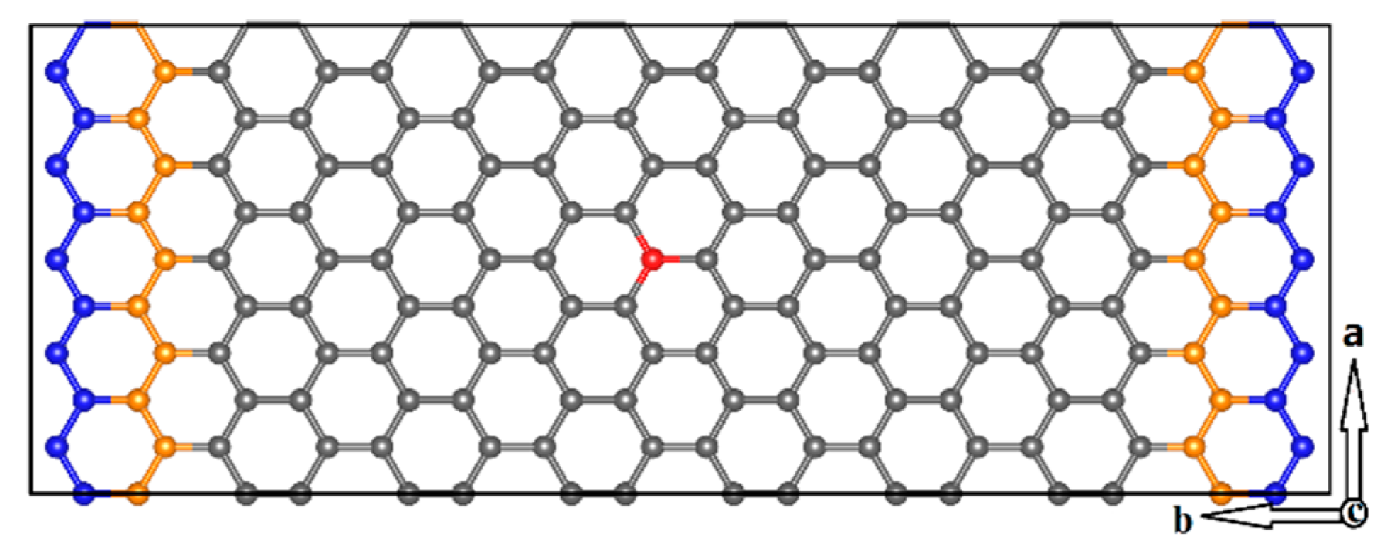
2. Methodology
3. Results and Discussion
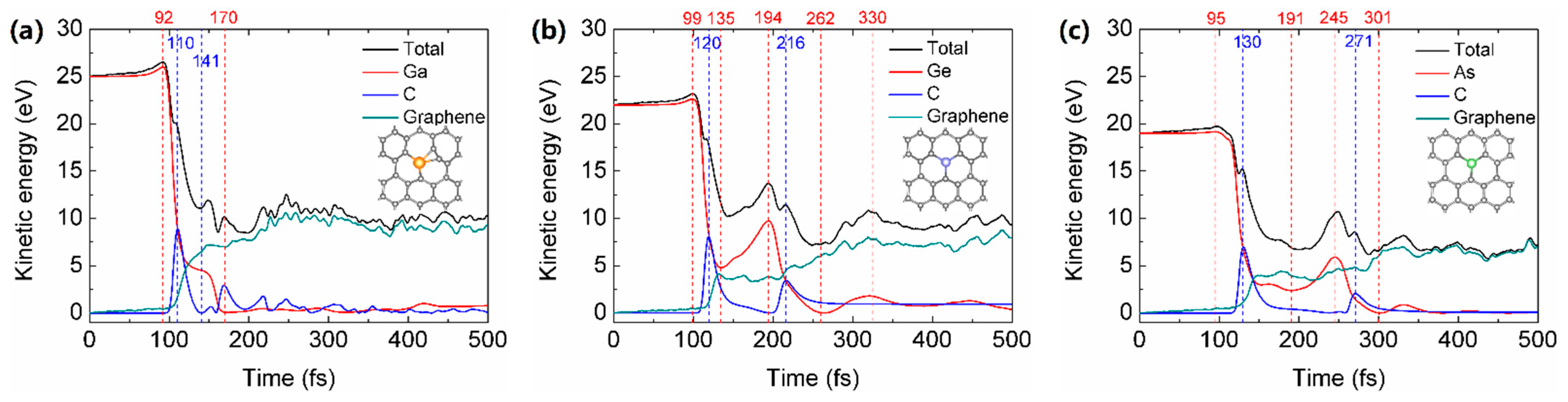
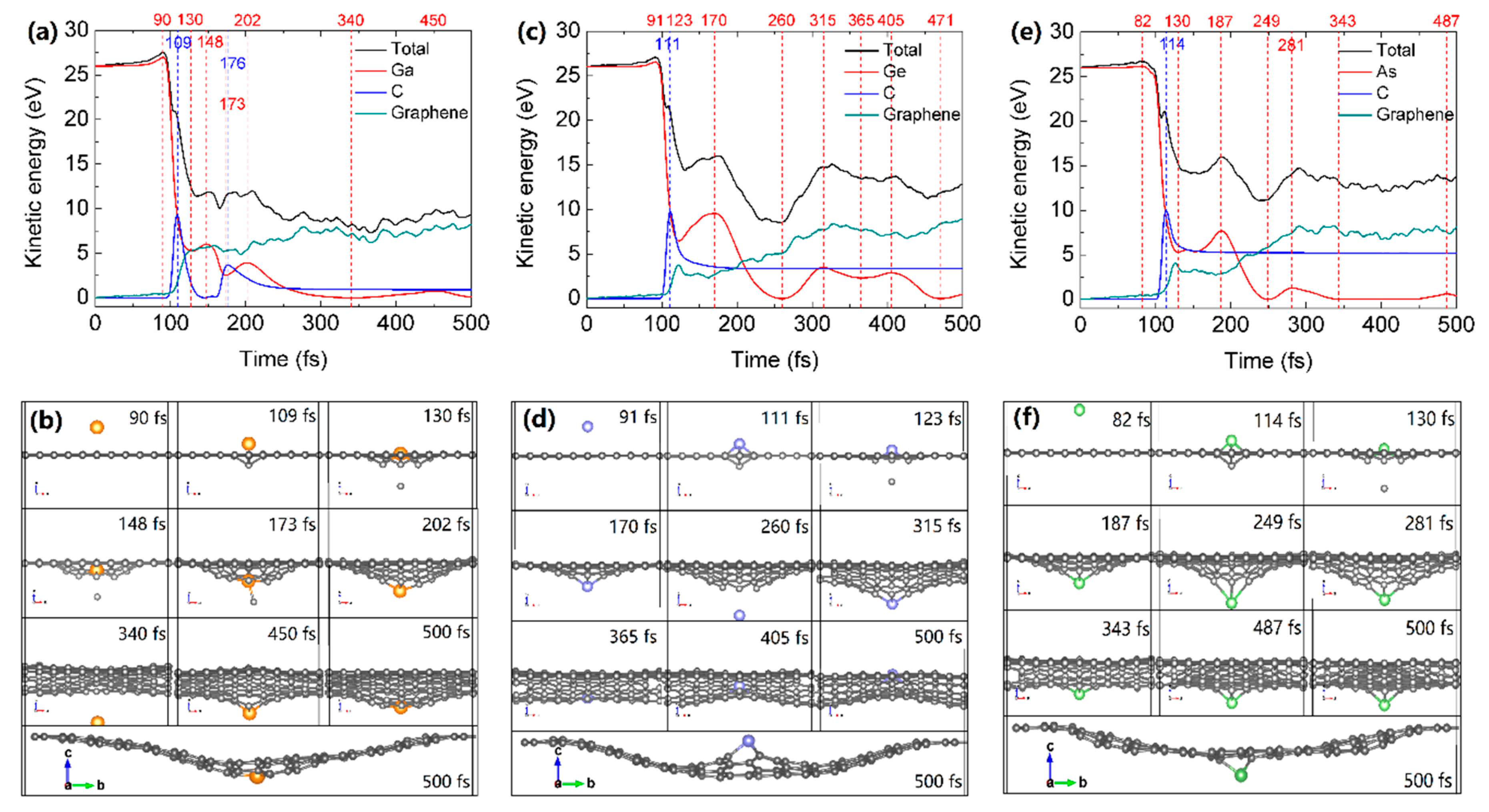
3.1. Evolution of Dynamical Process of Ga/Ge/As Atom Implanted into Graphene
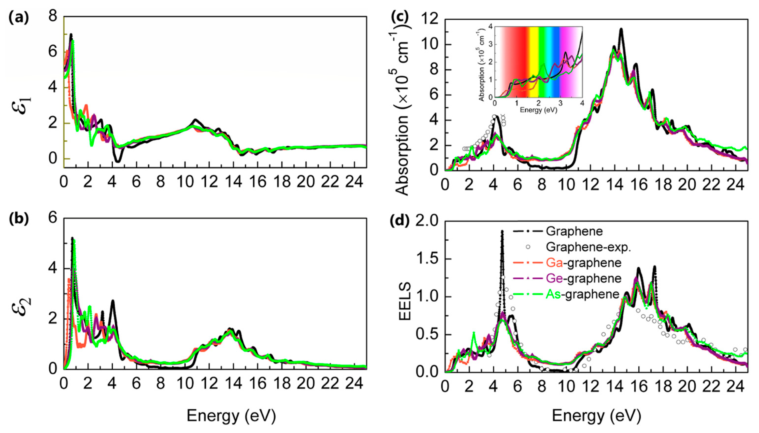
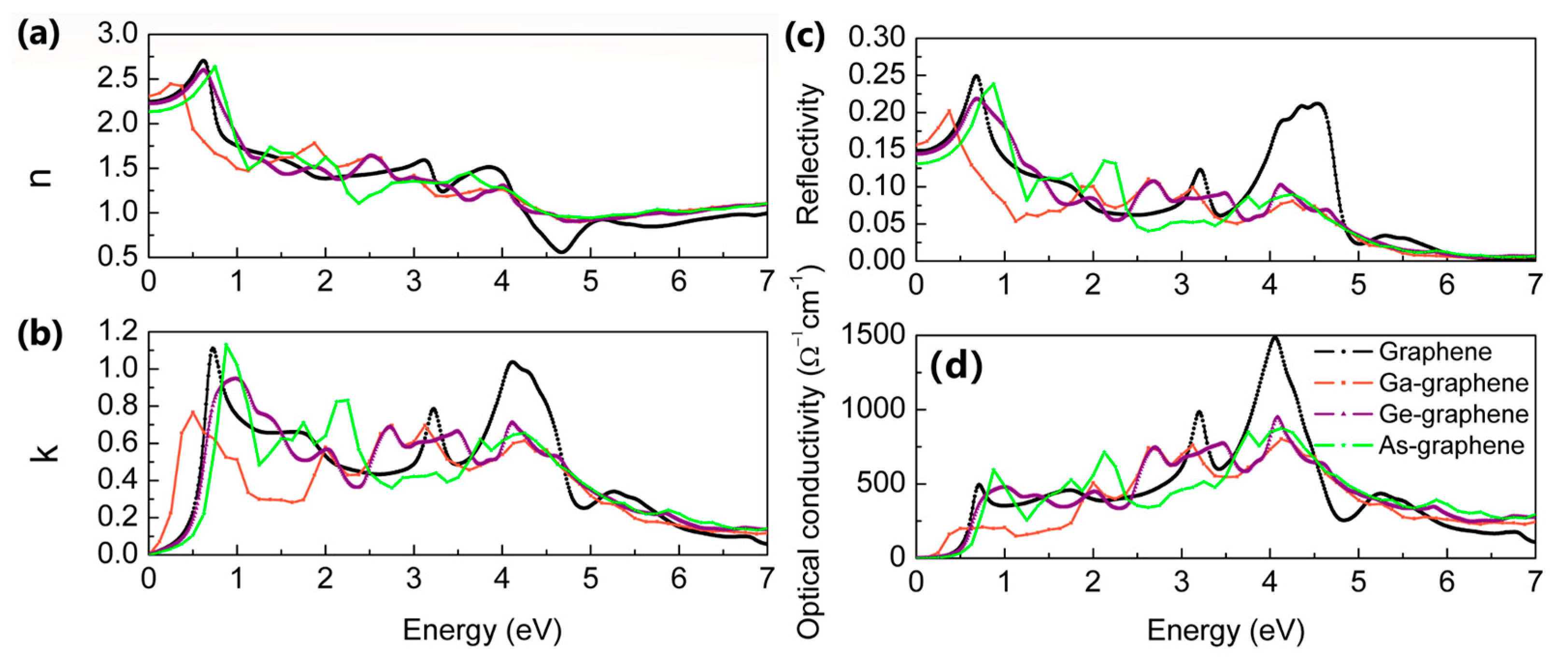
3.2. Electronic, Optical and Transport Properties of Implanted Ga/Ge/As-Graphene
4. Conclusions
Author Contributions
Funding
Institutional Review Board Statement
Informed Consent Statement
Data Availability Statement
Acknowledgments
Conflicts of Interest
References
- Bangert, U.; Pierce, W.; Kepaptsoglou, D.M.; Ramasse, Q.; Zan, R.; Gass, M.H.; Van den Berg, J.A.; Boothroyd, C.B.; Amani, J.; Hofsäss, H. Ion implantation of graphene-toward IC compatible technologies. Nano Lett. 2013, 13, 4902–4907. [Google Scholar] [CrossRef]
- Li, Z.; Chen, F. Ion beam modification of two-dimensional materials: Characterization, properties, and applications. Appl. Phys. Rev. 2017, 4, 011103–011124. [Google Scholar] [CrossRef]
- Schleberger, M.; Kotakoski, J. 2D material science: Defect engineering by particle irradiation. Material 2018, 11, 1885. [Google Scholar] [CrossRef] [PubMed] [Green Version]
- Wang, X.; Sun, G.; Routh, P.; Kim, D.-H.; Huang, W.; Chen, P. Heteroatom-doped graphene materials: Syntheses, properties and applications. Chem. Soc. Rev. 2014, 43, 7067–7098. [Google Scholar] [CrossRef] [PubMed] [Green Version]
- Åhlgren, E.H.; Kotakoski, J.; Krasheninnikov, A.V. Atomistic simulations of the implantation of low energy boron and nitrogen ions into graphene. Phys. Rev. B 2011, 83, 115424–115431. [Google Scholar] [CrossRef] [Green Version]
- Tripathi, M.; Markevich, A.; Böttger, R.; Facsko, S.; Besley, E.; Kotakoski, J.; Susi, T. Implanting germanium into graphene. ACS Nano 2018, 12, 4641–4647. [Google Scholar] [CrossRef] [Green Version]
- Åhlgren, E.H.; Markevich, A.; Besley, E. Atomistic simulations of the efficiencies of Ge and Pt ion implantation into graphene. J. Phys. Chem. C 2018, 122, 25700–25708. [Google Scholar] [CrossRef]
- Kepaptsoglou, D.; Hardcastle, T.P.; Seabourne, C.R.; Bangert, U.; Zan, R.; Amani, J.A.; Hofsäss, H.; Nicholls, R.J.; Brydson, R.M.D.; Scott, A.J.; et al. Electronic structure modification of ion implanted graphene: The spectroscopic signatures of p- and n-type doping. ACS Nano 2015, 9, 11398–11407. [Google Scholar] [CrossRef] [PubMed] [Green Version]
- Willke, P.; Amani, J.A.; Sinterhauf, A.; Thakur, S.; Kotzott, T.; Druga, T.; Weikert, S.; Maiti, K.; Hofsäss, H.; Wenderoth, M. Doping of graphene by low-energy ion beam implantation: Structural, electronic, and transport properties. Nano Lett. 2015, 15, 5110–5115. [Google Scholar] [CrossRef]
- Bangert, U.; Bleloch, A.; Gass, M.H.; Seepujak, A.; Van den Berg, J. Doping of few-layered graphene and carbon nanotubes using ion implantation. Phys. Rev. B 2010, 81, 245423–245434. [Google Scholar] [CrossRef]
- Zhao, W.; Höfert, O.; Gotterbarm, K.; Zhu, J.; Papp, C.; Steinrück, H.-P. Production of nitrogen-doped graphene by low-energy nitrogen implantation. J. Phys. Chem. C 2012, 116, 5062–5066. [Google Scholar] [CrossRef]
- Friedman, A.L.; Cress, C.D.; Schmucker, S.W.; Robinson, J.T.; Erve, O.M.J.V. Electronic transport and localization in nitrogen-doped graphene devices using hyperthermal ion implantation. Phys. Rev. B 2016, 93, 161409–161419. [Google Scholar] [CrossRef] [Green Version]
- Cress, C.D.; Schmucker, S.W.; Friedman, A.L.; Dev, P.; Culbertson, J.C.; Lyding, J.W.; Robinson, J.T. Nitrogen-doped graphene and twisted bilayer graphene via hyperthermal ion implantation with depth control. ACS Nano 2016, 10, 3714–3722. [Google Scholar] [CrossRef] [PubMed]
- Hofer, C.; Skákalová, V.; Görlich, T.; Tripathi, M.; Mittelberger, A.; Mangler, C.; Monazam, M.R.A.; Susi, T.; Kotakoski, J.; Meyer, J.C. Direct imaging of light-element impurities in graphene reveals triple-coordinated oxygen. Nat. Commun. 2019, 10, 4570–4578. [Google Scholar] [CrossRef] [PubMed] [Green Version]
- Susi, T.; Hardcastle, T.P.; Hofsäss, H.; Mittelberger, A.; Pennycook, T.J.; Mangler, C.; Brydson, R.D.; Scott, A.J.; Meyer, J.C.; Kotakoski, J. Single-atom spectroscopy of phosphorus dopants implanted into graphene. 2D Mater. 2016, 4, 021013–021020. [Google Scholar] [CrossRef]
- He, S.; Huang, C.; Liou, J.W.; Woon, W.Y.; Su, C.Y. Spectroscopic and electrical characterizations of low-damage phosphorous-doped graphene via ion implantation. ACS Appl. Mater. Interfaces 2019, 11, 47289–47298. [Google Scholar] [CrossRef]
- Lin, Y.C.; Teng, P.Y.; Yeh, C.H.; Koshino, M.; Chiu, P.W.; Suenaga, K. Structural and chemical dynamics of pyridinic-nitrogen defects in graphene. Nano Lett. 2015, 15, 7408–7413. [Google Scholar] [CrossRef] [PubMed]
- Zhao, S.; Xue, J. Tuning the band gap of bilayer graphene by ion implantation: Insight from computational studies. Phys. Rev. B 2012, 86, 165428–165438. [Google Scholar] [CrossRef]
- Bai, Z.; Zhang, L.; Liu, L. Improving low-energy boron/nitrogen ion implantation in graphene by ion bombardment at oblique angles. Nanoscale 2016, 8, 8761–8772. [Google Scholar] [CrossRef]
- Bai, Z.; Zhang, L.; Liu, L. Bombarding graphene with oxygen ions: Combining effects of incident angle and ion energy to control defect generation. J. Phys. Chem. C 2015, 119, 26793–26802. [Google Scholar] [CrossRef]
- Li, W.; Xue, J. Ion implantation of low energy Si into graphene: Insight from computational studies. RSC Adv. 2015, 5, 99920–99926. [Google Scholar] [CrossRef]
- Kantorovich, L.; Rompotis, N. Generalized Langevin equation for solids. II. Stochastic boundary conditions for nonequilibrium molecular dynamics simulations. Phys. Rev. B 2008, 78, 094305–094313. [Google Scholar] [CrossRef]
- Toton, D.; Lorenz, C.D.; Rompotis, N.; Martsinovich, N.; Kantorovich, L. Temperature control in molecular dynamic simulations of non-equilibrium processes. J. Phys. Condens. Matter. 2010, 22, 074205–074217. [Google Scholar] [CrossRef] [PubMed] [Green Version]
- Blöchl, P.E. Projector augmented-wave method. Phys. Rev. B 1994, 50, 17953–17979. [Google Scholar] [CrossRef] [PubMed] [Green Version]
- Perdew, J.P.; Chevary, J.A.; Vosko, S.H.; Jackson, K.A.; Pederson, M.R.; Singh, D.J.; Fiolhais, C. Atoms, molecules, solids, and surfaces: Applications of the generalized gradient approximation for exchange and correlation. Phys. Rev. B 1992, 46, 6671–6687. [Google Scholar] [CrossRef]
- Perdew, J.P.; Burke, K.; Ernzerhof, M. Generalized gradient approximation made simple. Phys. Rev. Lett. 1996, 77, 3865–3868. [Google Scholar] [CrossRef] [Green Version]
- Zhang, Y.; Yang, W. Comment on “Generalized gradient approximation made simple”. Phys. Rev. Lett. 1998, 80, 890. [Google Scholar] [CrossRef]
- Grimme, S. Semiempirical GGA-type density functional constructedwith a long-range dispersion correction. J. Comput. Chem. 2006, 27, 1787–1799. [Google Scholar] [CrossRef]
- Monkhorst, H.J.; Pack, J.D. Special points for Brillonin-zone integrations. Phys. Rev. B 1976, 13, 5188–5192. [Google Scholar] [CrossRef]
- Karpan, V.M.; Giovannetti, G.; Khomyakov, P.A.; Talanana, M.; Starikov, A.A.; Zwierzycki, M.; Van den Brink, J.; Brocks, G.; Kelly, P.J. Graphite and graphene as perfect spin filters. Phys. Rev. Lett. 2007, 99, 176602–176606. [Google Scholar] [CrossRef] [Green Version]
- Denis, P.A. Chemical reactivity and band-gap opening of graphene doped with gallium, germanium, arsenic, and selenium atoms. Chem. Phys. Chem. 2015, 15, 3994–4000. [Google Scholar] [CrossRef]
- Susi, T.; Hofer, C.; Argentero, G.; Leuthner, G.T.; Pennycook, T.J.; Mangler, C.; Meyer, J.C.; Kotakoski, J. Isotope analysis in the transmission electron microscope. Nat. Commun. 2016, 7, 13040–13050. [Google Scholar] [CrossRef]
- Langer, R.; Błoński, P.; Hofer, C.; Lazar, P.; Mustonen, K.; Meyer, J.C.; Susi, T.; Otyepka, M. Tailoring electronic and magnetic properties of graphene by phosphorus doping. ACS Appl. Mater. Interfaces 2020, 12, 34074–34085. [Google Scholar] [CrossRef] [PubMed]
- Gajdoš, M.; Hummer, K.; Kresse, G.; Furthmüller, J.; Bechstedt, F. Linear optical properties in the projector-augmented wave methodology. Phys. Rev. B 2006, 73, 045112–045121. [Google Scholar] [CrossRef] [Green Version]
- Wooten, F. Optical Properties of Solids; Academic Press: New York, NY, USA, 1972. [Google Scholar]
- Yu, P.; Cardona, M. Fundamentals of Semiconductors; Springer: Berlin, Germany, 1996. [Google Scholar]
- Ostovari, F.; Hasanpoori, M.; Abbasnejad, M.; Salehi, M.A. DFT calculations of graphene monolayer in presence of Fe dopant and vacancy. Physica B 2018, 541, 6–13. [Google Scholar] [CrossRef]
- Shahrokhi, M.; Leonard, C. Tuning the band gap and optical spectra of silicon-doped graphene: Many-body effects and excitonic states. J. Alloys Compd. 2017, 693, 1185–1196. [Google Scholar] [CrossRef]
- Fox, M. Optical Properties of Solids; Oxford Master Series in Condensed Matter Physics; Oxford University Press: Oxford, MS, USA, 2001. [Google Scholar]
- Antonov, V.N.; Yavorsky, B.Y.; Shpak, A.P.; Antonov, V.N.; Jepsen, O.; Guizzetti, G.; Marabelli, F.; Saha, S.; Sinha, T.P. Electronic structure and physical properties of NbSi2. Phys. Rev. B 1996, 53, 15631–15637. [Google Scholar] [CrossRef] [PubMed]
- Nair, R.R.; Ren, W.; Jalil, R.; Riaz, I.; Kravets, V.G.; Britnell, L.; Blake, P.; Schedin, F.; Mayorov, A.S.; Yuan, S.; et al. Fluorographene: A two-dimensional counterpart of Teflon. Small 2010, 6, 2877–2884. [Google Scholar] [CrossRef] [PubMed]
- Eberlein, T.; Bangert, U.; Nair, R.R.; Jones, R.; Gass, M.; Bleloch, A.L.; Novoselov, K.S.; Geim, A.; Briddon, P.R. Plasmon spectroscopy of free-standing graphene films. Phys. Rev. B 2008, 77, 233406–233410. [Google Scholar] [CrossRef] [Green Version]
- Rani, P.; Dubey, G.S.; Jindal, V.K. DFT study of optical properties of pure and doped Graphene. Phys. E 2014, 62, 28–35. [Google Scholar] [CrossRef] [Green Version]
- Long, M.; Tang, L.; Wang, D.; Li, Y.; Shuai, Z. Electronic structure and carrier mobility in graphdiyne sheet and nanoribbons: Theoretical predictions. ACS Nano 2011, 5, 2593–2600. [Google Scholar] [CrossRef]
- Zhao, Y.; Ma, Q.; Liu, B.; Yu, Z.; Yang, J.; Cai, M. Layer-dependent transport and optoelectronic property in two-dimensional perovskite: (PEA)2PbI4. Nanoscale 2018, 10, 8677–8688. [Google Scholar] [CrossRef] [PubMed]
- Hwang, E.H.; Sarma, S.D. Acoustic phonon scattering limited carrier mobility in 2D extrinsic graphene. Phys. Rev. B 2007, 77, 115449–115455. [Google Scholar] [CrossRef] [Green Version]
- Available online: http://www.matprop.ru/Si (accessed on 31 August 2021).
- Akinwande, D.; Huyghebaert, C.; Wang, C.; Serna, M.I.; Goossens, S.; Li, L.; Wong, H.-S.P.; Koppens, F.H.L. Graphene and two-dimensional materials for silicon technology. Nature 2019, 573, 507–518. [Google Scholar] [CrossRef]
- Cheng, J.; Du, J. Facile synthesis of germanium–graphene nanocomposites and their application as anode materials for lithium ion batteries. Cryst. Eng. Comm. 2012, 14, 397–400. [Google Scholar] [CrossRef]
- Zhong, C.; Wang, J.; Gao, X.; Wexler, D.; Liu, H. In situ one-step synthesis of a 3D nanostructured germanium–graphene composite and its application in lithium-ion batteries. J. Mater. Chem. A 2013, 1, 10798–10804. [Google Scholar] [CrossRef] [Green Version]
- Ullah, S.; Shi, Q.; Zhou, J.; Yang, X.; Ta, H.; Hasan, M.; Ahmad, N.M.; Fu, L.; Bachmatiuk, A.; Rümmeli, M.H. Advances and trends in chemically doped graphene. Adv. Mater. Interfaces 2020, 7, 2000999–2001022. [Google Scholar] [CrossRef]
- Chen, H.; Zhang, X.; Zhang, Y.; Wang, D.; Bao, D.; Que, Y.; Xiao, W.; Du, S.; Yang, M.; Pantelides, S.T.; et al. Atomically precise, custom-design origami graphene nanostructures. Science 2019, 365, 1036–1040. [Google Scholar] [CrossRef] [Green Version]
- Ne, M.L.O.; Abbassi, A.; El Hachimi, A.G.; Benyoussef, A.; Ez-Zahraouy, H.; El Kenz, A. Electronic optical, properties and widening band gap of graphene with Ge doping. Opt. Quant. Electron. 2017, 49, 218–231. [Google Scholar]
- Gecim, G.; Ozekmekci, M.; Fellah, M.F. Ga and Ge-doped graphene structures: A DFT study of sensor applications for methanol. Comput. Theor. Chem. 2020, 1180, 112828–112839. [Google Scholar] [CrossRef]
- Losurdo, M.; Yi, C.; Suvorova, A.; Rubanov, S.; Kim, T.H.; Giangregorio, M.M.; Jiao, W.Y.; Bergmair, I.; Bruno, G.; Brown, A.S. Demonstrating the capability of the high-performance plasmonic gallium–graphene couple. ACS Nano 2014, 8, 3031–3041. [Google Scholar] [CrossRef] [PubMed]
- Krasheninnikov, A.V.; Nordlund, K. Ion and electron irradiation-induced effects in nanostructured materials. J. Appl. Phys. 2010, 107, 071301–071371. [Google Scholar] [CrossRef]


| Atomic Type | Emax (eV) | Emin (eV) | Td (eV) |
|---|---|---|---|
| Ga of 25 eV | 8.9 (110 fs) | 0 (140 fs) | 8.9 |
| Ga of 26 eV | 9.3 (109 fs) | 0 (145 fs) | 9.3 |
| Ge of 22 eV | 8.1 (120 fs) | 0 (196 fs) | 8.1 |
| Ge of 26 eV | 9.7 (111 fs) | 3.4 (211 fs) | 6.4 |
| As of 19 eV | 6.9 (130 fs) | 0 (238 fs) | 6.9 |
| As of 26 eV | 9.9 (114 fs) | 5.3 (174 fs) | 4.6 |
| Type | Carrier | E1 (eV) | C (J m−2) | m* (me) | μ (cm2 V−1·s−1) |
|---|---|---|---|---|---|
| Graphene | h | −6.600 | 385.804 | −0.021 | 4.50 × 10⁵ |
| e | 6.574 | 385.804 | 0.021 | 4.40 × 10⁵ | |
| Ga-graphene | h | −6.167 | 274.608 | −0.038 | 2.72 × 10⁴ |
| e | −4.339 | 274.608 | 0.037 | 5.73 × 10⁴ | |
| Ge-graphene | h | 2.710 | 296.811 | −0.073 | 4.04 × 10⁴ |
| e | −2.892 | 296.811 | 0.115 | 1.50 × 10⁴ | |
| As-graphene | h | −2.130 | 306.125 | −0.244 | 6.06 × 10³ |
| e | −2.940 | 306.125 | 0.113 | 1.48 × 10⁴ |
Publisher’s Note: MDPI stays neutral with regard to jurisdictional claims in published maps and institutional affiliations. |
© 2021 by the authors. Licensee MDPI, Basel, Switzerland. This article is an open access article distributed under the terms and conditions of the Creative Commons Attribution (CC BY) license (https://creativecommons.org/licenses/by/4.0/).
Share and Cite
Ren, F.; Yao, M.; Li, M.; Wang, H. Tailoring the Structural and Electronic Properties of Graphene through Ion Implantation. Materials 2021, 14, 5080. https://doi.org/10.3390/ma14175080
Ren F, Yao M, Li M, Wang H. Tailoring the Structural and Electronic Properties of Graphene through Ion Implantation. Materials. 2021; 14(17):5080. https://doi.org/10.3390/ma14175080
Chicago/Turabian StyleRen, Fei, Mengli Yao, Min Li, and Hui Wang. 2021. "Tailoring the Structural and Electronic Properties of Graphene through Ion Implantation" Materials 14, no. 17: 5080. https://doi.org/10.3390/ma14175080