Abstract
Atomic layer deposition (ALD) technology has unlocked new ways of manipulating the growth of inorganic materials. The fine control at the atomic level allowed by ALD technology creates the perfect conditions for the inclusion of new cationic or anionic elements of the already-known materials. Consequently, novel material characteristics may arise with new functions for applications. This is especially relevant for inorganic luminescent materials where slight changes in the vicinity of the luminescent centers may originate new emission properties. Here, we studied the luminescent properties of CaS:Eu by introducing europium with oxygen ions by ALD, resulting in a novel CaS:EuO thin film. We study structural and photoluminescent properties of two different ALD deposited Eu doped CaS thin films: Eu(thd)3 which reacted with H2S forming CaS:Eu phosphor, or with O3 originating a CaS:EuO phosphor. It was found that the emission wavelength of CaS:EuO was 625.8 nm whereas CaS:Eu was 647 nm. Thus, the inclusion of O2− ions by ALD in a CaS:Eu phosphor results in the blue-shift of 21.2 nm. Our results show that ALD can be an effective way to introduce additional elements (e.g., anionic elements) to engineer the physical properties (e.g., inorganic phosphor emissions) for photonics and optoelectronics.
1. Introduction
The development of new luminescent materials and optoelectronic devices such as lamps, displays, lasers, solar cells and photodetectors, relies strongly on the flexibility of the used fabrication technique. The need for higher material quality and versatility in the fabrication of optoelectronic devices was one of the main motivations that lead to the birth and development of atomic layer deposition (ALD) [1,2]. As an example, in the early days of ALD, inorganic phosphors such as ZnS:M (M = Mn, Tb, Tm), SrS:M (M = Ce, Cu, Tb, Pb), CaS:M (M = Eu, Ce, Tb, Pb), were extensively researched for the development of thin film electroluminescent displays (TFEL) [3].
ALD takes a relevant role in the synthetization of inorganic phosphors. The self-limiting mechanism of ALD allows the growth of one atomic layer at the time, consequently leading to accurate control of the thin film thickness and the ability to create multilayer structures [4]. Furthermore, the meticulous inclusion of dopants can be conducted in a single fabrication run, while the host material is being grown. These effects are particularly interesting regarding the doping level control of thin film materials. Thus, they are appropriate for the fabrication of inorganic phosphors, where the doping element acts as a luminescent center. It is known that if the luminescent centers are close to each other it can lead to concentration quenching. However, using ALD, the spatial distance between the luminescent centers can be controlled. The distance is restrained by the steric hindrance effect of the ligands [5,6,7,8]. With this distribution engineering procedure, higher doping concentrations can be achieved in comparison to other fabrication techniques [7], which may reflect in higher luminance values.
In recent years, ALD technology has been used to explore new ways of combining atomic elements to develop materials with unorthodox characteristics. As a result, the research of single-anion (homo-anionic) compounds, such as pure metal oxides, pnictides (nitrides, arsenides, phosphides) or chalcogenides (sulfides, selenides, tellurides), has given place to a mixed anion-centered (multi-anion or hetero-anionic) compounds research [9]. Mixed anion centered materials include for example carbonitrides [10], oxyfluorides [11], oxynitrides [12], oxycarbides [13], and oxysulfides [14]. The ability to incorporate different types of anions allows to change a variety of material properties and characteristics. Electron configuration, electronegativity, size, charge and polarization of this anionic species can lead to the creation of unique structural, chemical, electronic, optical, and magnetic states. In such materials, ALD technique grants the fine-tuning between the combination of cations and multiple anions in thin films [9].
A good example of ALD multi-anion research applied to luminescent materials is a previous study on the control europium of the oxidation state in a Y2O3−xSX matrix [14]. In this research, it was demonstrated that the oxidation state of Eu luminescent center could be changed by the introduction of Eu atoms with an ALD sub cycle of two different anion precursors: either H2S or O3. The distinct oxidation states of the luminescent center led to different emission spectrums of the Y2O3−xSX:Eu phosphor.
Inspired by the previous report, we continue to explore the ALD fabrication potential. More specifically, the ability of shifting the peak emission of calcium sulfide doped with europium (CaS:Eu), a well-known red emitting inorganic phosphor material. CaS:Eu luminescent characteristics have been widely studied and used in a variety of applications such as, medical imaging [15,16], cell labeling [17], white-light-emitting diodes [18,19] and electroluminescent devices [20,21,22,23]. The red emission in CaS:Eu is originated from the Eu divalent state of ionization (Eu2+) and its broad emission is caused by electron transition from the lower 4f65d1 state to the 4f7 ground state [24]. This transition in a CaS host originates an emission with wavelength range from 600 to 750 nm and with a peak emission at 650 nm.
In the present article, it is shown that the peak emission of CaS:Eu can be shifted using ALD method. The shift can occur by introducing localized oxygen atoms in the phosphor matrix. Hence, the inorganic phosphor emission was compared between two different structures, (1) pure CaS:Eu, where Eu is exposed to H2S reducing gas, and (2) CaS:EuO, where Eu in exposed to O3 oxidating gas during the material growth. In comparison to the CaS:Eu phosphor, CaS:EuO reveals a red peak emission towards shorter wavelengths. Similar tuning effects of the CaS:Eu emission has been previously reported by adding alkaline earth metals such as strontium [25,26], magnesium and barium to the reaction mixture [27]. However, we present a study where the tuning is performed by adding oxygen anions reinforcing the idea that ALD can be used to modify the vicinity of the dopant elements. These materials fabricated by ALD can thus be used for applications where the fine color tuning is advantageous such as: red electroluminescent devices [20,21,22,23,28], white-light-emitting diodes [18,19] solar cells [29], and lasers [6,8,30].
2. Materials and Methods
Film growth was performed using atomic layer deposition in a Beneq TFS-200 ALD-reactor (Beneq Oy, Espoo, Finland). The reactor pressure was around 2 mbar during the process and the temperature was kept at 300 °C. N2 was used as a carrier and purge gas. All films were grown on (100)-Si substrates coated with 10 nm of Al2O3 thin film. Trimethylaluminum (TMA, Al(CH3)3) (98%, Strem Chemicals UK Ltd., Cambridge, UK) and H2O were used to grow Al2O3 coating film. All CaS based thin films were grown using β-diketonate precursors: Ca(thd)2 (99%. Volatec, Porvoo, Finland) and Eu(thd)3 (99.5%, Intatrade, Anhalt-Bitterfeld Germany) (THD = 2,2,6,6-tetramethyl-3,5-heptanedionate). Ca(thd)2 was kept at 205 °C while Eu(thd)3 was kept at 185 °C with a vapor pressure of 133 Pa [31]. Ca(thd)2 vapor pressure is unknown in literature. CaS matrix was formed by reacting Ca(thd)2 with H2S using 350 pulses of each chemical. After the first 350 pulses, Eu(thd)3 was introduced as a doping agent by pulsing either H2S or O3. Two cycles of Eu(thd)3 followed by H2S were used in one of the samples. A sequence of three O3 pulses intercalated by two pulses of Eu(thd)3 were used in the other sample. A schematic representation of the doping sequences used in the two samples can be seen in Figure 1. Both phosphor layers were grown using 6 layers of CaS intercalated by five Eu layers, resulting in approximately 100 nm thin film. Finally, another 10 nm layer of Al2O3 was used to coat the europium doped CaS thin films. Thus, two different samples were studied in this work: Al2O3/CaS:Eu/Al2O3/Si and Al2O3/CaS:EuO/Al2O3/Si, denominated from now on as CaS:Eu and CaS:EuO, respectively. Table 1 summarizes the pulsing sequence, pulse and purge times, and the respective number of cycles.
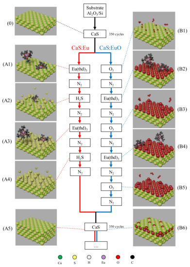
Figure 1.
Schematic of ALD doping sequence used in CaS:Eu and CaS:EuO samples. (0) Top layers of CaS matrix. Red track represents the doping sequence in CaS:Eu sample including: (A1) Eu(thd)3 pulsing on CaS layer, (A2) H2S pulsing after nitrogen purge, (A3) second Eu(thd)3 pulsing after purge, (A4) H2S pulsing after nitrogen purge and (A5) CaS monolayer after the doping sequence. Blue track represents the doping sequence in CaS:EuO sample including: (B1) O3 pulse on CaS layer, (B2) Eu(thd)3 pulsing after purge, (B3) second O3 pulsing after nitrogen purge, (B4) second Eu(thd)3 pulsing after purge, (B5) third O3 pulsing after nitrogen purge and (B6) CaS monolayer after the doping sequence. Atomic elements are represented with the following colors: (Ca) green, (S) yellow, (H) gray, (Eu) lavender, (O) red and (C) black.

Table 1.
Pulsing sequences and respective pulsing times, number of cycles per layer for CaS:Eu and CaS:EuO phosphor layers.
The growth per cycle (GPC) of Al2O3, CaS, Eu2O3 was determined individually by using a SE400adv ellipsometer (SENTECH Instruments GmbH, Berlin, Germany) with a 633 nm wavelength at 70° angle of incidence. The crystallinity of europium doped CaS thin films was investigated by X-ray diffraction (XRD) using the Cu Kα line in a Rigaku SmartLab (Rigaku Europe SE, Neu-Isenburg, Germany) high-resolution X-ray diffractometer. Data acquired by the XRD were analyzed using the HighScore Plus 4.6 (PANalytical B.V., Almelo, The Netherlands). The X-ray photoelectron spectroscopy (XPS) measurements were made using Kratos Axis Ultra system (Kratos Analytical Ltd., Manchester, UK), equipped with a monochromatic Al Kα X-ray source. All measurements were performed with 0.3 mm × 0.7 mm analysis area. The wide scans were performed with 80 eV pass energy and 1 eV energy step, and the high-resolution scans were performed with 40 eV pass energy at 0.1 eV steps. Eu doped CaS samples were analyzed with elastic recoil detection analysis (ERDA) using a 13.6 MeV 63Cu7+ ion beam. The investigated area was approximately 2 × 2 mm2. The measurement was carried out with a 70° angle between the sample normal and beam, whereas the scattering angle was 40.6°. Time-of-flight–energy (ToF-E) telescope was used to detect the recoiling atoms from the sample. Photoluminescence (PL) emission of Eu doped CaS thin films was measured with a Hitachi F-7100 Fluorescence Spectrophotometer (Hitachi High-Tech Analytical Science Ltd., Abingdon, UK) equipped with a 150 W xenon lamp. Measurements were performed at room temperature with a photomultiplier tube voltage of 400 V, with a bandwidth of 10 nm.
3. Results
3.1. Crystallinity
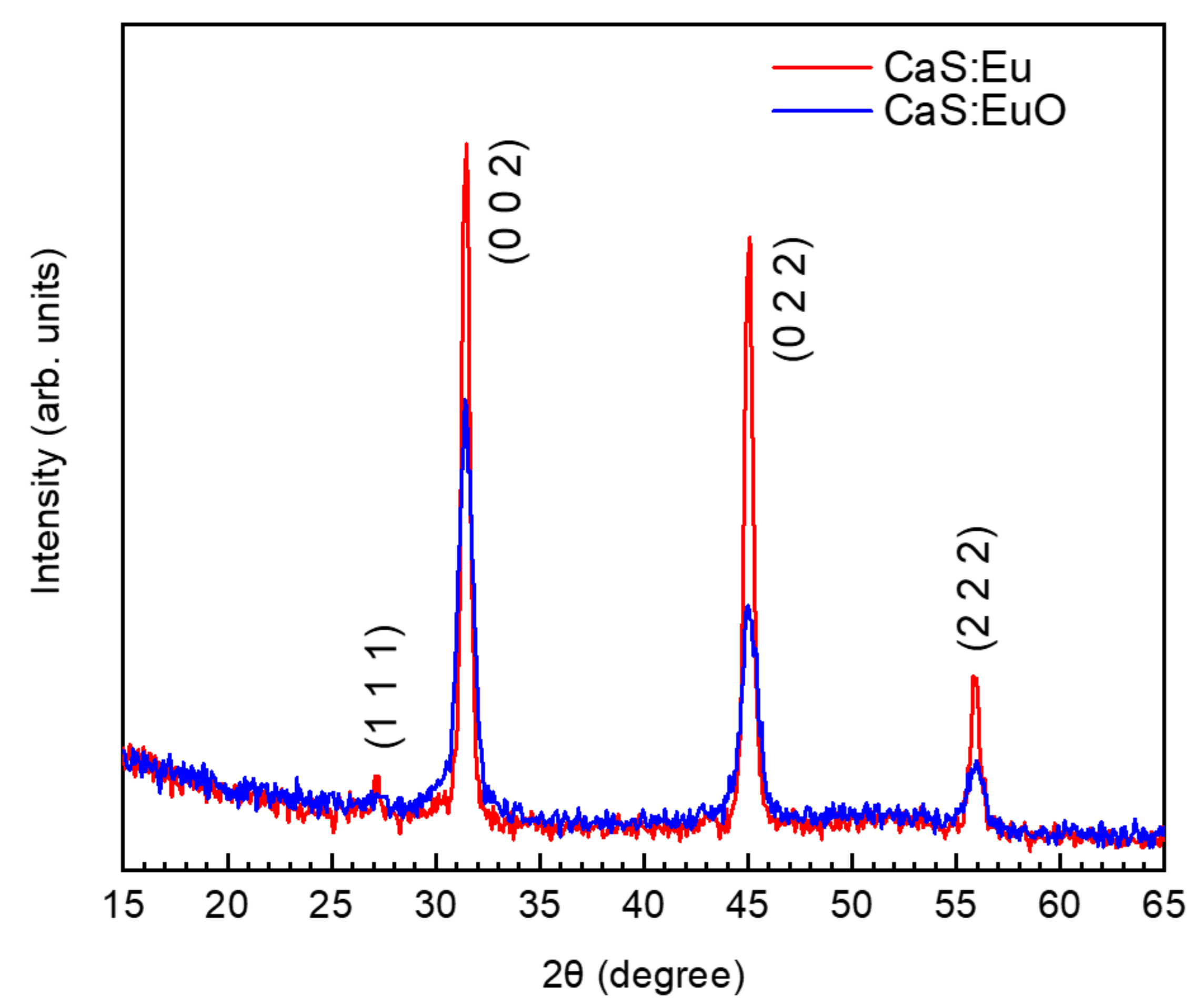
Figure 2 illustrates grazing incidence XRD patterns for CaS:Eu and CaS:EuO thin films measured between 15° and 65°. XRD patterns were carried out with an incidence angle of 2°. The grazing incident XRD data for both thin films show a main polycrystalline phase (randomly orientated). The identified peaks are related to (1 1 1), (0 0 2), (0 2 2) and (2 2 2) reflections. The peak position and the order of peak intensity are similar to the one reported by cross-reference COD:96-900-8607 [32]. Thus, indicating that CaS:Eu and CaS:EuO have a cubic structure with Fmm space group. The lattice parameter was determined to be a = 5.68 Å and a = 5.69 Å for CaS:Eu and CaS:EuO, respectively. Furthermore, CaS:Eu shows a higher level of crystallinity compared to CaS:EuO thin film.
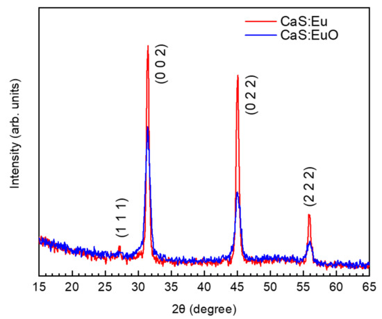
Figure 2.
Grazing incidence XRD of CaS:Eu and CaS:EuO samples.
3.2. Chemical Analysis
XPS was performed on both CaS:Eu and CaS:EuO samples. We used argon ion etching to remove the 10 nm Al2O3 top coating layer prior to detailed analysis of the materials. The removal of the oxide was followed by XPS measurements after 100 s, 200 s, 400 s, 600 s and 1000 s of ion etching. In the CaS:Eu sample the Al 2p peak disappeared after 600 s whereas in the CaS:EuO sample the Al 2p intensity decreased by a factor of four after 1000 s.
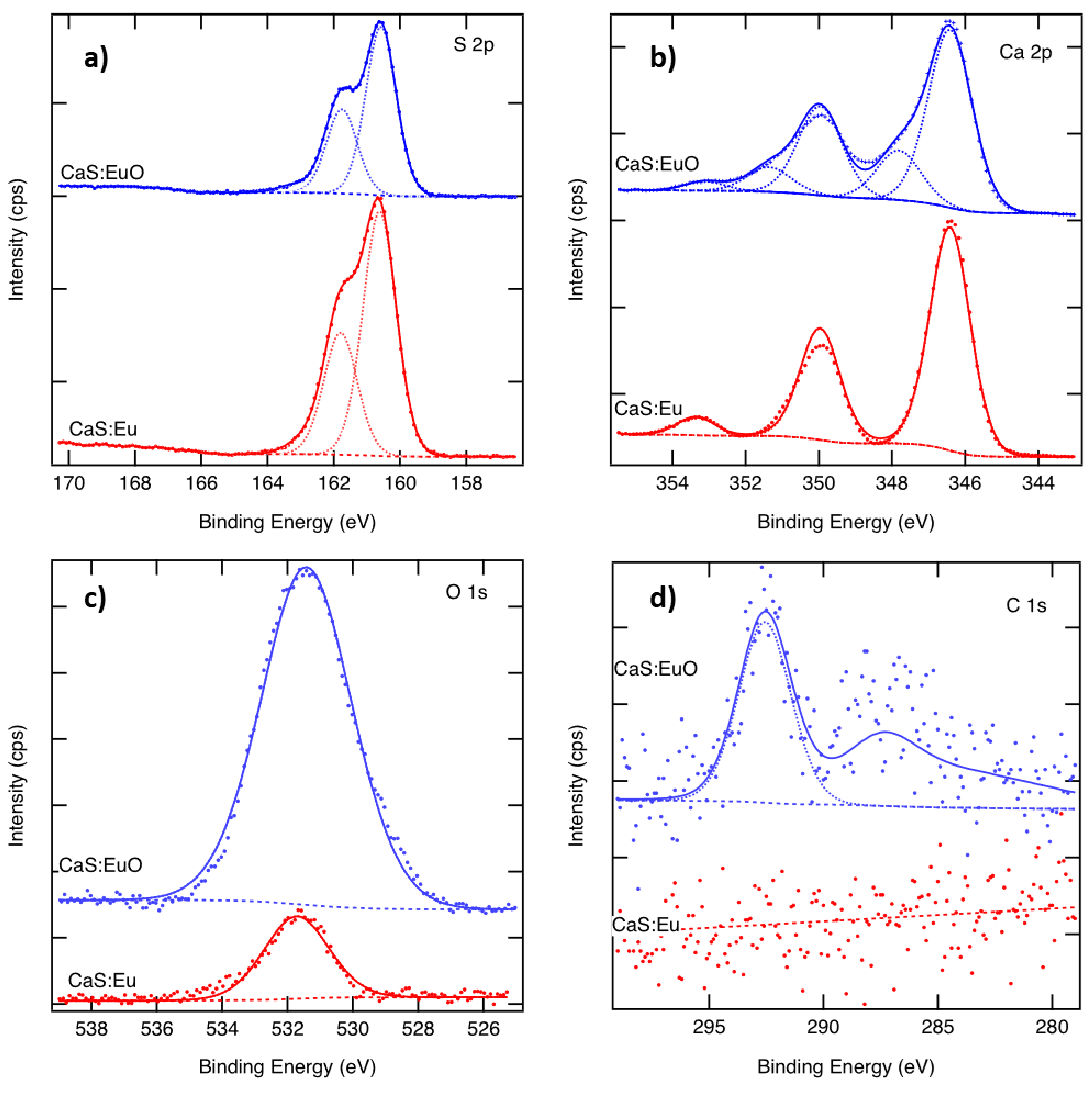
The S 2p spectra of CaS:Eu and CaS:EuO in Figure 3a, show a typical doublet with 1.18 eV separation. The S 2p binding energy of 160.7 eV indicates the presence of sulfides, whereas the sulfate component around 169 eV is missing [33]. The Ca 2p spectra of both samples are illustrated in Figure 3b. The CaS:Eu spectrum shows a typical doublet with 3.55 eV separation. The Ca 2p3/2 binding energy of 346.4 eV corresponds to CaS or CaO. In the CaS:EuO sample, an additional component related to the CaCO3 or CaSO4 is seen at 347.9 eV, with a peak area corresponding to 20% of the total Ca. As there is no sulphate peak in the S 2p spectra, we call this peak CaCO3 although the binding energy would better fit to 348.0 eV of CaSO4 than (347.1 ± 0.3) eV of CaCO3 [33]. The fitting also includes a satellite peak above 353 eV in both samples. Figure 3c shows the measured O 1s spectra. There is only one peak appearing at 531.6 eV in both samples, indicating similar oxygen. However, the O 1s signal from CaS:EuO indicates 42 at-% of oxygen whereas that of the CaS:Eu only 10 at-%. Figure 3d shows the C 1s spectra. The CaS:Eu sample does not contain carbon. In the CaS:EuO sample a small C 1s peak around 292 eV is seen. This peak can be related to CO3 groups. There might also be some structure above the noise level around 286 eV. The amount of carbon in the CaS:EuO sample is below 2 at-%.

Figure 3.
Measured and fitted (a) S 2p, (b) Ca 2p and (c) O 1s and (d) C 1s spectra of CaS:Eu and CaS:EuO samples.
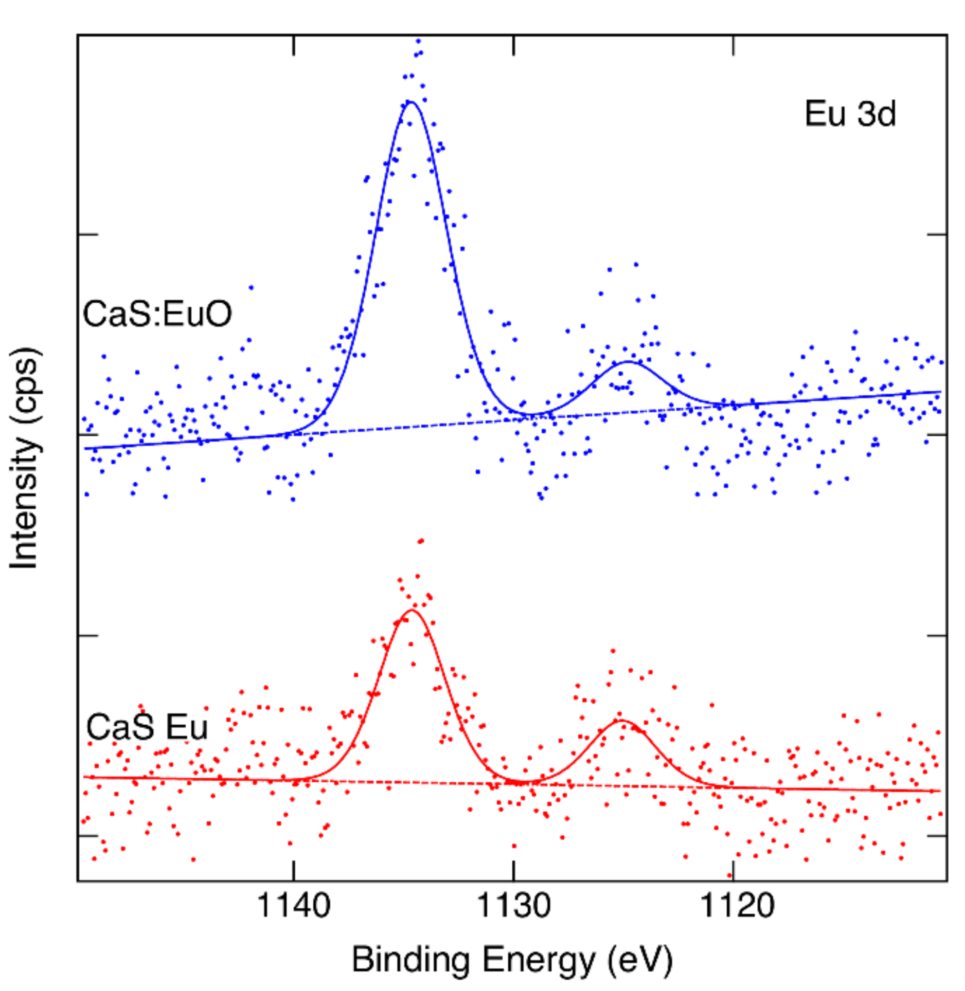
Figure 4 illustrate the Eu 3d core levels of CaS:Eu and CaS:EuO, respectively. Eu3+ and Eu2+ oxidation states can be identified in both samples if we accept binding energies 1134.4 eV and 1124.7 eV for the components [34]. However, the data are noisy despite of the long measurement time used. We can estimate that the Eu3+/Eu2+ ratio is approximately 5/2 in CaS:Eu whereas in CaS:EuO it is close to 6/1.
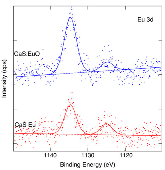
Figure 4.
Measured and fitted Eu 3d spectra of CaS:Eu and CaS:EuO samples.
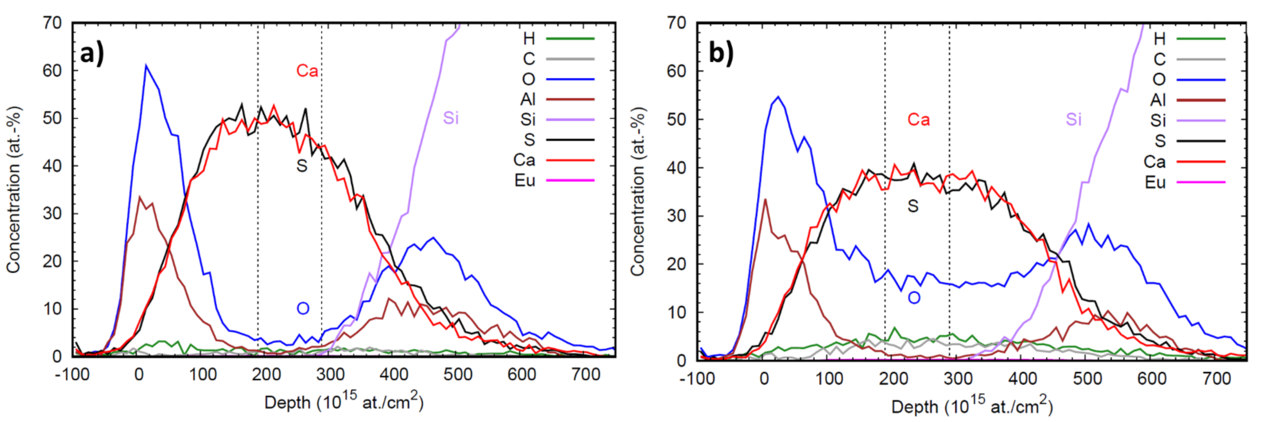
Figure 5a,b illustrates the elemental depth profile obtained by ToF-ERDA measurements of CaS:Eu and CaS:EuO samples, respectively. The depth resolution degrades deeper in the sample due to energy loss straggling. Therefore, the elemental composition of both europium doped CaS layers was analyzed by selecting an interval representative of the film bulk, with no Al and high concentration of Ca and S. The vertical lines in the depth profile plots indicate the depth range from which the averages in Table 2 are calculated.
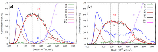
Figure 5.
Depth profile of (a) CaS:Eu and (b) CaS:EuO samples. Dashed vertical lines indicate the depth range used for elemental compositional analysis.
Table 2.
Elemental composition of the CaS:Eu and CaS:EuO samples measured with ToF-ERDA.
Table 2 shows a comparison between the element composition of CaS:Eu and CaS:EuO layers. In both films, the atomic percentages of S and Ca are approximately the same, demonstrating that CaS is present with a stoichiometry of 1:1. The doping level is higher for samples where Eu is grown on CaS with ozone. As expected, the level of oxygen present in the doped layer is higher when ozone is used to introduce Eu(thd)3. However, in the sample where no ozone was used there is still a low concentration of oxygen impurities. Both H and C contamination levels were higher in the CaS:EuO sample.
3.3. Photoluminescence
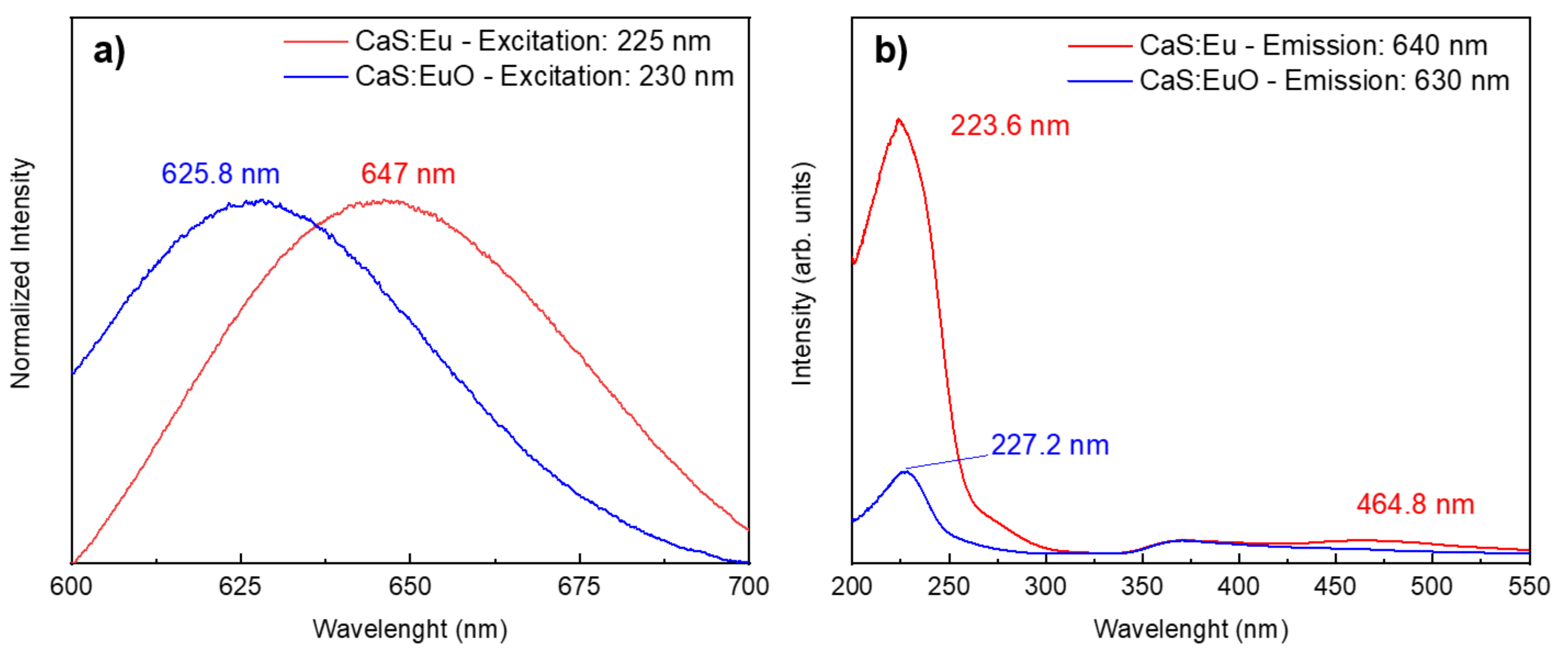
The normalized PL spectra were plotted in Figure 6a to facilitate the comparison between the maximum emission wavelength of CaS:Eu and CaS:EuO samples. Both photoluminescent emission spectra were measured between 600 and 700 nm and excited with approximated wavelengths values correspondent to the maximum emission intensity. The CaS:Eu sample has a maximum emission value of 647 nm, when excited with a wavelength of 225 nm. The maximum emission is related to the Eu2+ ion Laporte allowed transition, from 4f6 5d1 to the 4f7 (8S7/2), characteristic of CaS:Eu2+ materials [24]. In addition, CaS:EuO sample shows a maximum peak emission of 625.8 nm, for an excitation wavelength of 230 nm. The PL measurements were carried out in three different CaS:EuO samples for reproducibility proposes. All tree samples showed similar behavior.
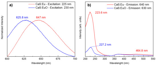
Figure 6.
(a) Normalized emission spectra and (b) excitation spectra from CaS:Eu and CaS:EuO, measured at room temperature.
Furthermore, photoluminescent excitation (PLE) spectra in Figure 6b were registered by monitoring the emission at 640 nm and 630 nm for CaS:Eu and CaS:EuO samples, respectively. All samples show a broad excitation band between 200 and 300 nm, which can be associated with the Eu2+ 4f7 (8S7/2) → 4f6 5d1 [Eg] and valence-to-conduction band transitions. Whereas the low intensity excitation band in CaS:Eu sample from 400 to 550 nm is related to Eu2+ 4f7 → 4f6 5d1 [t2g] transition [35]. This transition is believed to have too low intensity to be detected in CaS:EuO sample, therefore it was not used to excite the samples.
A summary of Figure 6a,b is presented in Table 3, which include the excitation and absorption wavelength; excitation and emission peak; and respective intensities. In Table 3, it is clear that CaS:Eu sample has higher intensities in comparison to CaS:EuO sample, regarding excitation and emission peaks.
Table 3.
Summary of the CaS:Eu and CaS:EuO emission and excitation data acquired from the photoluminescent measurements.
4. Discussion
With the data acquired from XPS it is possible to assume that the Al from the top coating layer can be measured until 600 s of argon sputtering, in CaS:Eu sample. Thus, leading to the conclusion that beyond the 600 s etching step, a nearly pure CaS:Eu layer can be found. Faint traces of oxygen can still be analyzed within the europium doped CaS layer. These traces of oxygen could originate from the O diffusion of the Al2O3 top coating layer into the CaS:Eu layer. In this case, the oxygen contamination can occur due to the slow ALD fabrication process at 300 °C. Additionally, due to the high Ca affinity towards oxygen atoms, there is the possibility of O present in the β-diketonate molecule to be adsorbed on the CaS surface, upon Eu(thd)3 and H2S reaction. The same oxygen contamination can be visualized in the ToF-ERDA analysis, see Table 2. As expected, the presence of oxygen in CaS:EuO sample can be identified clearly after the 600 s due to the intentional introduction of O atoms. XPS analysis of sulfur species revealed that sulfur is detected in form of sulfide and no sulfates are present in the phosphor layer.
Furthermore, the results from XPS and ToF-ERDA show higher level of carbon content within the CaS:EuO sample. These data are supported by the detection of CaCO3 component in Figure 3b and higher carbon concentration shown in Table 2. The carbon contamination in CaS:EuO could be explained by the reaction between ozone and the β-diketonate precursor (Eu(thd)3), which is known to originate carbonates in the films [14]. Additionally, the ToF-ERDA analysis revealed a lower hydrogen presence in CaS:Eu, which indicates the excellent reactivity between Ca(thd)2 and Eu(thd)3 with H2S. These efficient surface reactions are responsible to effectively remove lighter species, such as H [36]. In contrast, higher levels of carbon and hydrogen contamination in CaS:EuO sample can be correlated with the lower reactivity of O3 species with Ca(thd)2 and Eu(thd)3, in comparison to H2S. Moreover, the intentional inclusion of oxygen atoms into the europium doped CaS layer may be the major responsible factor for the lower level of crystallinity. The presence of O2− can cause distortions in the CaS crystal lattice leading to structural defects. Nonetheless, the crystal structure of CaS:EuO is still similar to CaS:Eu and no traces of CaO or CaSOx polycrystalline phases are identified.
It was found that the oxidation level ratio of Eu3+/Eu2+ is higher in the CaS:EuO samples. The higher Eu3+ ion presence correlates with the presence of O2− ions, which is expected since Eu tends to oxidize to its trivalent form whenever enough oxygen atoms are available. Furthermore, the europium doping level was revealed to be slightly higher when Eu(thd)3 was grown on the CaS layer with ozone instead of H2S. This difference in the doping level may be explained by the facilitated introduction of Eu atoms when there is a monolayer of oxygen present in the CaS surface. Oxygen has higher electronegativity than sulfur and thus increases the probability of Eu adsorption. Note that, Eu(thd)3 is pulsed into the ALD reactor chamber after an O3 pulse. In a previous study it was stated that Eu may be more reactive towards the H2S in comparison to ozone, and thus increasing the doping level [14]. However, in the present study, the surface has an oxygen monolayer instead of a sulfur monolayer, prior to the Eu(thd)3 pulse. The oxygen presence in the surface may be a determinant factor for the Eu growth rate as a dopant, as it may increase the adsorption of Eu(thd)3.
The different emission wavelengths of CaS:Eu and CaS:EuO samples can be explained by the presence of O2− ion in the phosphor layer. It is probable that O2− ion inclusion originated structural defects in the CaS structure. This can be concluded due to the lower intensity of the PL emission in the CaS:EuO sample, since certain defects may decrease luminance. Additionally, the defects may have distorted the crystal structure which led to a larger lattice constant, assuming a value of 5.69 Å instead of 5.68 Å in the presence of O2− ions. The larger lattice constant may indicate that the distance between Eu2+ cations and the anions increase. The larger distance between Eu2+ cations and the anions lead to a decrease in the crystal-field strength [25,26]. Therefore, the addition of a O2− ion originates a decrease in the energy difference between t2g and the Eg states of the 4f6 5d1 electronic configuration, thus leading to blue-shifted emission. Figure 7 illustrates a schematic of Eu2+ energy level as function of the crystal-field. Several factors may explain the lower emission intensity of the CaS:EuO sample in comparison to CaS:Eu, such as slightly lower Eu concentration and lower crystallinity.
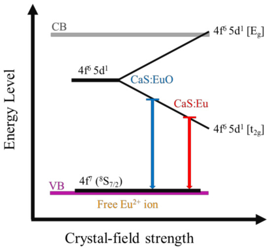
Figure 7.
Schematic energy diagram of Eu²⁺ 5d level splitting as function of crystal-field strength in CaS:Eu and CaS:EuO samples.
5. Conclusions
In this work, two samples of Eu doped CaS phosphors were grown by ALD. Structural, chemical, compositional and emission properties of both samples were correlated with the fabrication conditions. XRD analysis shows the polycrystalline nature of the phosphor layers with a slight difference in the lattice dimension and level of crystallinity between the samples. XPS was used to detect the chemical bounds between the ionic species present in the phosphor layer. Additionally, ToF-ERDA accurately identify the levels of contamination originated during the ALD fabrication process. It was shown that the inclusion of Eu together with oxygen as a dopant in the CaS matrix reduces the overall crystal-field strength, which leads to blue-shifted emission by 21.2 nm in comparison to the CaS:Eu sample. The peak emission is found at 625.8 nm for CaS:EuO, whereas CaS:Eu shows the typical emission around 647 nm. These results show that by introducing oxygen anion in the CaS:Eu thin film using ALD method, the resulting phosphor emission can be modified.
Author Contributions
Conceptualization, J.R., Z.S. and H.L.; formal analysis, J.R., J.L. and J.J.; investigation, J.R., J.L., J.J., Z.S. and H.L.; writing—original draft preparation, J.R.; writing—review and editing, J.R., Z.S. and H.L.; supervision, H.L. All authors have read and agreed to the published version of the manuscript.
Funding
The work in this paper was funded by the European Union’s Horizon 2020 Research and Innovation Program under the Marie Sklodowska-Curie Grant Agreement No 76495. Z.S. and H.L. acknowledge funding from the Academy of Finland Flagship Programme, Photonics Research and Innovation (PREIN), Decision Number: 320167. Z.S. thanks the European Union’s Horizon 2020 Research and Innovation Program (820423,S2QUIP; 965124, FEMTOCHIP), the EU H2020-MSCA-RISE-872049 (IPN-Bio), Business Finland (ALDEL), and ERC (834742).
Institutional Review Board Statement
Not applicable.
Informed Consent Statement
Not applicable.
Data Availability Statement
Data sharing is not applicable to this article.
Acknowledgments
The authors would like to thank Saoussen Merdes and Jani Holopainen for the constructive discussions.
Conflicts of Interest
The authors declare no conflict of interest. The funders had no role in the design of the study; in the collection, analyses, or interpretation of data; in the writing of the manuscript; or in the decision to publish the results.
References
- Puurunen, R.L. A Short History of Atomic Layer Deposition: Tuomo Suntola’s Atomic Layer Epitaxy. Chem. Vap. Depos. 2014, 20, 332–344. [Google Scholar] [CrossRef] [Green Version]
- Leskelä, M.; Mattinen, M.; Ritala, M. Review Article: Atomic layer deposition of optoelectronic materials. J. Vac. Sci. Technol. B 2019, 37, 030801. [Google Scholar] [CrossRef] [Green Version]
- Ritala, M.; Leskela, M. Chapter 2: Atomic Layer Deposition; Academic Press: San Diego, CA, USA, 2002; ISBN 0-12-512909-2. [Google Scholar]
- Ritala, M.; Kukli, K.; Rahtu, A.; Räisänen, P.I.; Leskelä, M.; Sajavaara, T.; Keinonen, J. Atomic Layer Deposition of Oxide Thin Films with Metal Alkoxides as Oxygen Sources. Science 2000, 288, 319–321. [Google Scholar] [CrossRef] [PubMed]
- Van, T.T.; Chang, J.P. Controlled erbium incorporation and photoluminescence of Er-doped Y2O3. Appl. Phys. Lett. 2005, 87, 11907. [Google Scholar] [CrossRef]
- Rönn, J.; Karvonen, L.; Kauppinen, C.; Perros, A.P.; Peyghambarian, N.; Lipsanen, H.; Säynätjoki, A.; Sun, Z. Atomic Layer Engineering of Er-Ion Distribution in Highly Doped Er:Al2O3 for Photoluminescence Enhancement. ACS Photon 2016, 3, 2040–2048. [Google Scholar] [CrossRef]
- Scarafagio, M.; Tallaire, A.; Chavanne, M.-H.; Cassir, M.; Ringuedé, A.; Serrano, D.; Goldner, P.; Ferrier, A. Improving the Luminescent Properties of Atomic Layer Deposition Eu: Y2O3 Thin Films through Optimized Thermal Annealing. Phys. Status Solidi A 2020, 217, 1–7. [Google Scholar] [CrossRef]
- Rönn, J.; Zhang, W.; Autere, A.; Leroux, X.; Pakarinen, L.; Alonso-Ramos, C.; Säynätjoki, A.; Lipsanen, H.; Vivien, L.; Cassan, E.; et al. Ultra-high on-chip optical gain in erbium-based hybrid slot waveguides. Nat. Commun. 2019, 10, 432. [Google Scholar] [CrossRef] [PubMed] [Green Version]
- Tripathi, T.S.; Karppinen, M. Mixed-Anion Compounds: An Unexplored Playground for ALD Fabrication. Adv. Mater. Interfaces 2021, 8, 2100146. [Google Scholar] [CrossRef]
- Cho, G.; Rhee, S.-W. Plasma Enhanced Atomic Layer Deposition of TiCxNyFilm with Various Reactive Gases. ECS J. Solid State Sci. Technol. 2014, 3, P185–P191. [Google Scholar] [CrossRef] [Green Version]
- Choi, Y.-J.; Park, H.-H. A simple approach to the fabrication of fluorine-doped zinc oxide thin films by atomic layer deposition at low temperatures and an investigation into the growth mode. J. Mater. Chem. C 2014, 2, 98–108. [Google Scholar] [CrossRef]
- Tao, J.-J.; Ma, H.-P.; Yuan, K.-P.; Gu, Y.; Lian, J.-W.; Li, X.-X.; Huang, W.; Nolan, M.; Lu, H.-L.; Zhang, D.-W. Modification of 1D TiO2 nanowires with GaOxNy by atomic layer deposition for TiO2@GaOxNy core–shell nanowires with enhanced photoelectrochemical performance. Nanoscale 2020, 12, 7159–7173. [Google Scholar] [CrossRef]
- Closser, R.G.; Bergsman, D.S.; Bent, S.F. Molecular Layer Deposition of a Highly Stable Silicon Oxycarbide Thin Film Using an Organic Chlorosilane and Water. ACS Appl. Mater. Interfaces 2018, 10, 24266–24274. [Google Scholar] [CrossRef]
- Rosa, J.; Deuermeier, J.; Soininen, P.J.; Bosund, M.; Zhu, Z.; Fortunato, E.; Martins, R.; Sugiyama, M.; Merdes, S. Control of Eu Oxidation State in Y2O3−xSx:Eu Thin-Film Phosphors Prepared by Atomic Layer Deposition: A Structural and Photoluminescence Study. Materials 2019, 13, 93. [Google Scholar] [CrossRef] [PubMed] [Green Version]
- Burbano, D.C.R.; Sharma, S.K.; Dorenbos, P.; Viana, B.; Capobianco, J.A. Persistent and Photostimulated Red Emission in CaS:Eu2+,Dy3+ Nanophosphors. Adv. Opt. Mater. 2015, 3, 551–557. [Google Scholar] [CrossRef]
- Gao, Y.; Li, R.; Zheng, W.; Shang, X.; Wei, J.; Zhang, M.; Xu, J.; You, W.; Chen, Z.; Chen, X. Broadband NIR photostimulated luminescence nanoprobes based on CaS:Eu2+,Sm3+ nanocrystals. Chem. Sci. 2019, 10, 5452–5460. [Google Scholar] [CrossRef] [PubMed] [Green Version]
- Wang, J.; Zhu, Y.; Grimes, C.A.; Cai, Q. Multicolor lanthanide-doped CaS and SrS near-infrared stimulated luminescent nanoparticles with bright emission: Application in broad-spectrum lighting, information coding, and bio-imaging. Nanoscale 2019, 11, 12497–12501. [Google Scholar] [CrossRef]
- Suresh, K.; Murthy, K.V.R.; Rao, A.; Poornachandra, R.N.V. Rare Earth Doped Alkali Earth Sulfide Phosphors for White-Light LEDs. ISRN Condens. Matter Phys. 2011, 2011, 392917. [Google Scholar] [CrossRef] [Green Version]
- Guo, C.; Huang, D.; Su, Q. Methods to improve the fluorescence intensity of CaS:Eu2+ red-emitting phosphor for white LED. Mater. Sci. Eng. B 2006, 130, 189–193. [Google Scholar] [CrossRef]
- Tanaka, K.; Mikami, A.; Ogura, T.; Taniguchi, K.; Yoshida, M.; Nakajima, S. High brightness red electroluminescence in CaS:Eu thin films. Appl. Phys. Lett. 1986, 48, 1730–1732. [Google Scholar] [CrossRef]
- Abe, Y.; Onisawa, K.-I.; Ono, Y.A.; Hanazono, M. Effects of Oxygen in CaS:Eu Active Layers on Emission Properties of Thin Film Electroluminescent Cells. Jpn. J. Appl. Phys. 1990, 29, 1495–1498. [Google Scholar] [CrossRef]
- Poelman, D.; Vercaemst, R.; van Meirhaeghe, R.; Laflère, W.; Cardon, F. Influence of the growth conditions on the properties of CaS:Eu electroluminescent thin films. J. Lumin 1997, 75, 175–181. [Google Scholar] [CrossRef]
- Poelman, D.; van Haecke, J.E.; Smet, P. Advances in sulfide phosphors for displays and lighting. J. Mater. Sci. Mater. Electron. 2009, 20, 134–138. [Google Scholar] [CrossRef]
- Dorenbos, P. Energy of the first 4f7→4f65d transition of Eu2+ in inorganic compounds. J. Lumin. 2003, 104, 239–260. [Google Scholar] [CrossRef]
- Sung, H.J.; Cho, Y.S.; Huh, Y.; Do, Y. Preparation, Characterization and Photoluminescence Properties of Ca1-xSrxS:Eu Red-emitting Phosphors for a White LED. Bull. Korean Chem. Soc. 2007, 28, 1280–1284. [Google Scholar] [CrossRef] [Green Version]
- Lin, J.; Huang, Y.; Mi, J.; Zhang, X.; Lu, Z.; Xu, X.; Fan, Y.; Zou, J.; Tang, C. BN-coated Ca1−xSrxS:Eu solid-solution nanowires with tunable red light emission. Nanotechnology 2013, 24, 405701. [Google Scholar] [CrossRef]
- Sun, B.; Yi, G.; Chen, D.; Zhou, Y.; Cheng, J. Synthesis and characterization of strongly fluorescent europium-doped calcium sulfide nanoparticles. J. Mater. Chem. 2002, 12, 1194–1198. [Google Scholar] [CrossRef]
- Rosa, J.; Heikkilä, M.; Sirkiä, M.; Merdes, S. Red Y2O3:Eu-Based Electroluminescent Device Prepared by Atomic Layer Deposition for Transparent Display Applications. Materials 2021, 14, 1505. [Google Scholar] [CrossRef] [PubMed]
- Getz, M.N.; Hansen, P.-A.; Fjellvåg, H.; Nilsen, O. Luminescent properties of europium titanium phosphate thin films deposited by atomic layer deposition. RSC Adv. 2017, 7, 8051–8059. [Google Scholar] [CrossRef] [Green Version]
- Rönn, J.; Zhang, J.; Zhang, W.; Tu, Z.; Matikainen, A.; le Roux, X.; Durán-Valdeiglesias, E.; Vulliet, N.; Boeuf, F.; Ramos, C.A.; et al. Erbium-doped hybrid waveguide amplifiers with net optical gain on fully industrial 300 mm silicon nitride photonic platform. Opt. Express 2020, 28, 27919. [Google Scholar] [CrossRef]
- Sicre, J.E.; Dubois, J.T.; Eisentraut, K.J.; Sievers, R.E. Volatile lanthanide chelates. II. Vapor pressures, heats of vaporization, and heats of sublimation. J. Am. Chem. Soc. 1969, 91, 3476–3481. [Google Scholar] [CrossRef]
- Wyckoff, R.W.G. Crystal Structures, 2nd ed.; Interscience Publishers: New York, NY, USA, 1963. [Google Scholar]
- Naumkin, A.V.; Kraut-Vass, A.; Gaarenstroom, S.W.; Powell, C.J. NIST X-ray Photoelectron Spectroscopy Database, NIST Standard Reference Database Number 20. Available online: https://srdata.nist.gov/xps/citation.aspx (accessed on 2 September 2021).
- Liu, W.-Q.; Wu, D.; Chang, H.; Duan, R.-X.; Wu, W.-J.; Amu, G.; Chao, K.-F.; Bao, F.-Q.; Tegus, O. The Enhanced Red Emission and Improved Thermal Stability of CaAlSiN3:Eu2+ Phosphors by Using Nano-EuB6 as Raw Material. Nanomaterials 2018, 8, 66. [Google Scholar] [CrossRef] [PubMed] [Green Version]
- Nyenge, R.; Swart, H.; Ntwaeaborwa, O. Luminescent properties, intensity degradation and X-ray photoelectron spectroscopy analysis of CaS:Eu2+ powder. Opt. Mater. 2015, 40, 68–75. [Google Scholar] [CrossRef]
- Dezelah, C.L.; Myllymäki, P.; Päiväsaari, J.; Arstila, K.; Niinistö, L.; Winter, C.H. The growth of ErxGa2−xO3 films by atomic layer deposition from two different precursor systems. J. Mater. Chem. 2007, 17, 1308–1315. [Google Scholar] [CrossRef]


Publisher’s Note: MDPI stays neutral with regard to jurisdictional claims in published maps and institutional affiliations. |
© 2021 by the authors. Licensee MDPI, Basel, Switzerland. This article is an open access article distributed under the terms and conditions of the Creative Commons Attribution (CC BY) license (https://creativecommons.org/licenses/by/4.0/).