
Piezoelectric A15B16C17 Compounds and Their Nanocomposites for Energy Harvesting and Sensors: A Review


Abstract
:1. Introduction
2. Materials and Methods
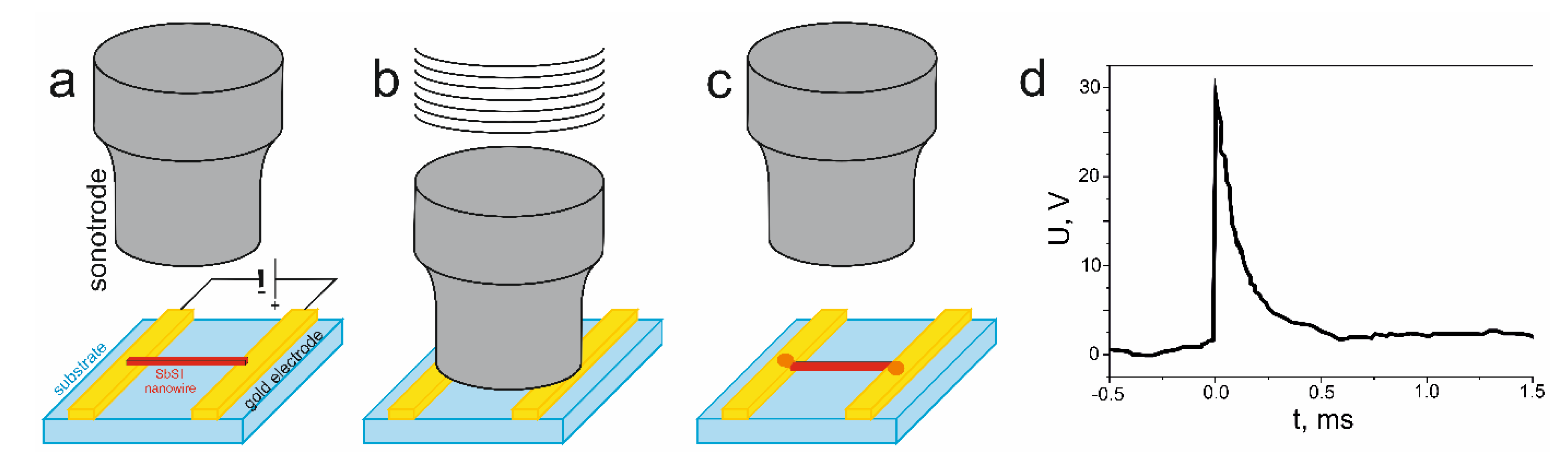
2.1. A15B16C17 Nanowires Synthesis
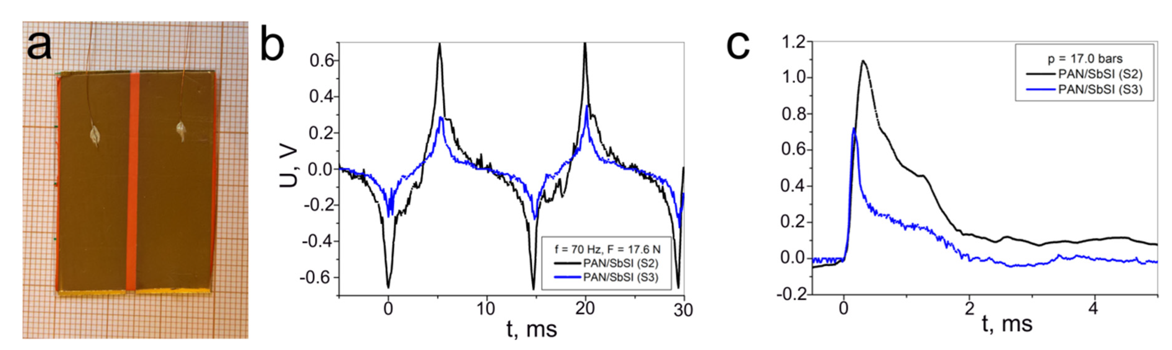
2.2. PAN/SbSI Composite
2.3. Cellulose/SbSI Composite
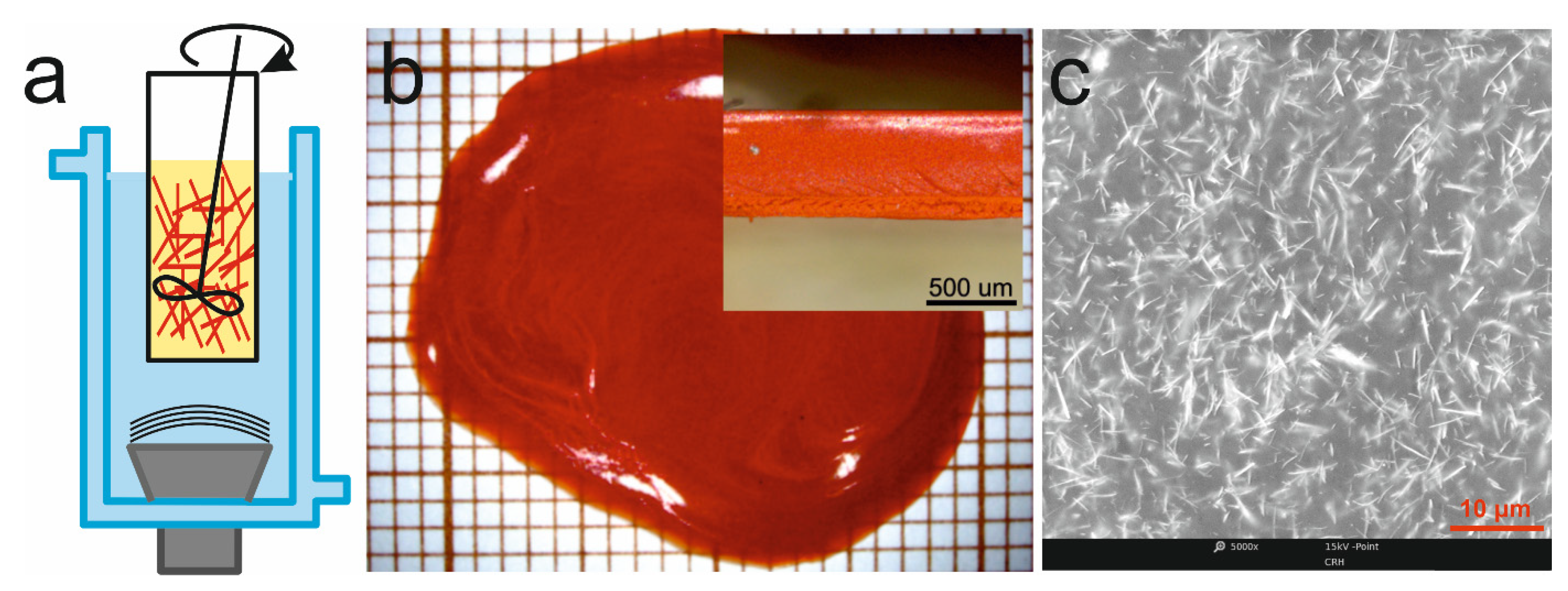
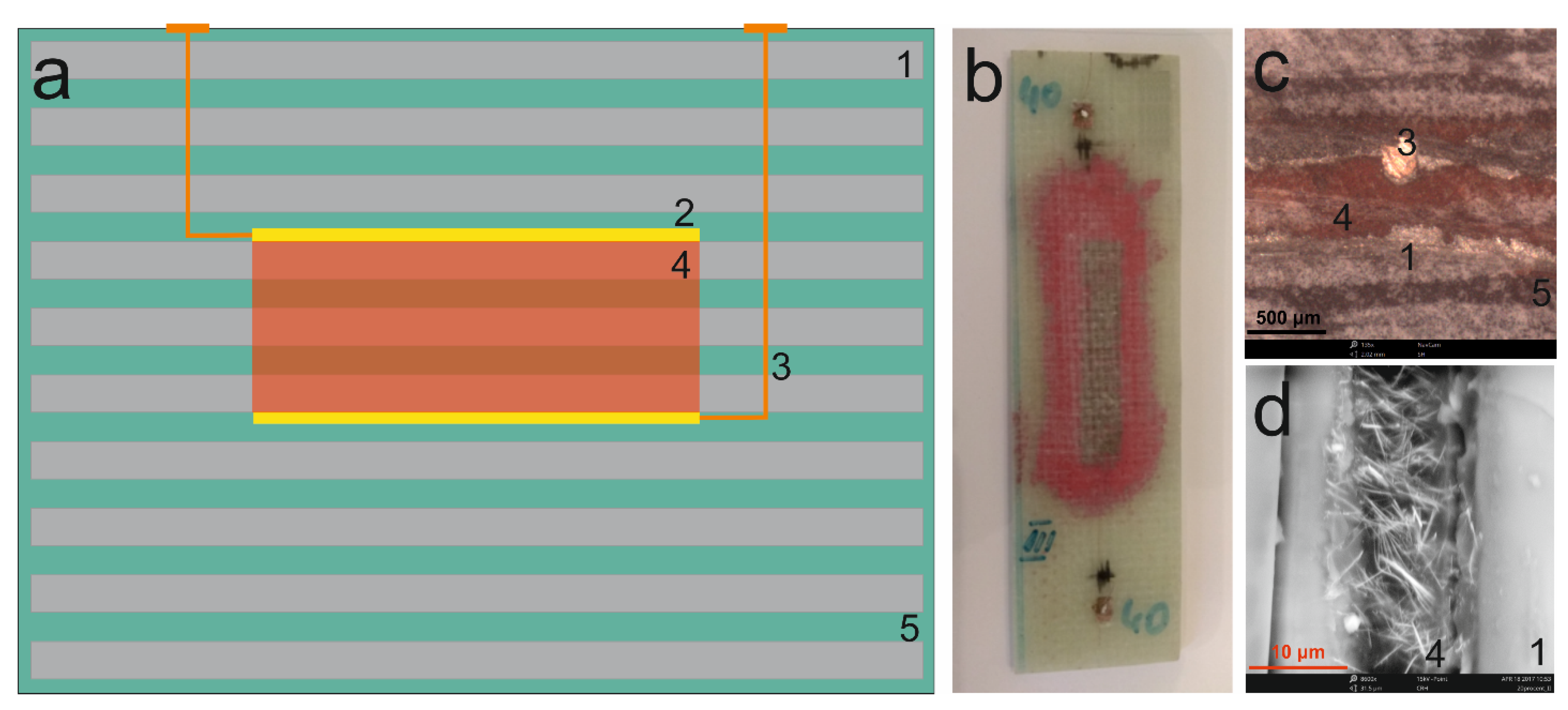
2.4. Epoxy Resin/SbSI Composite
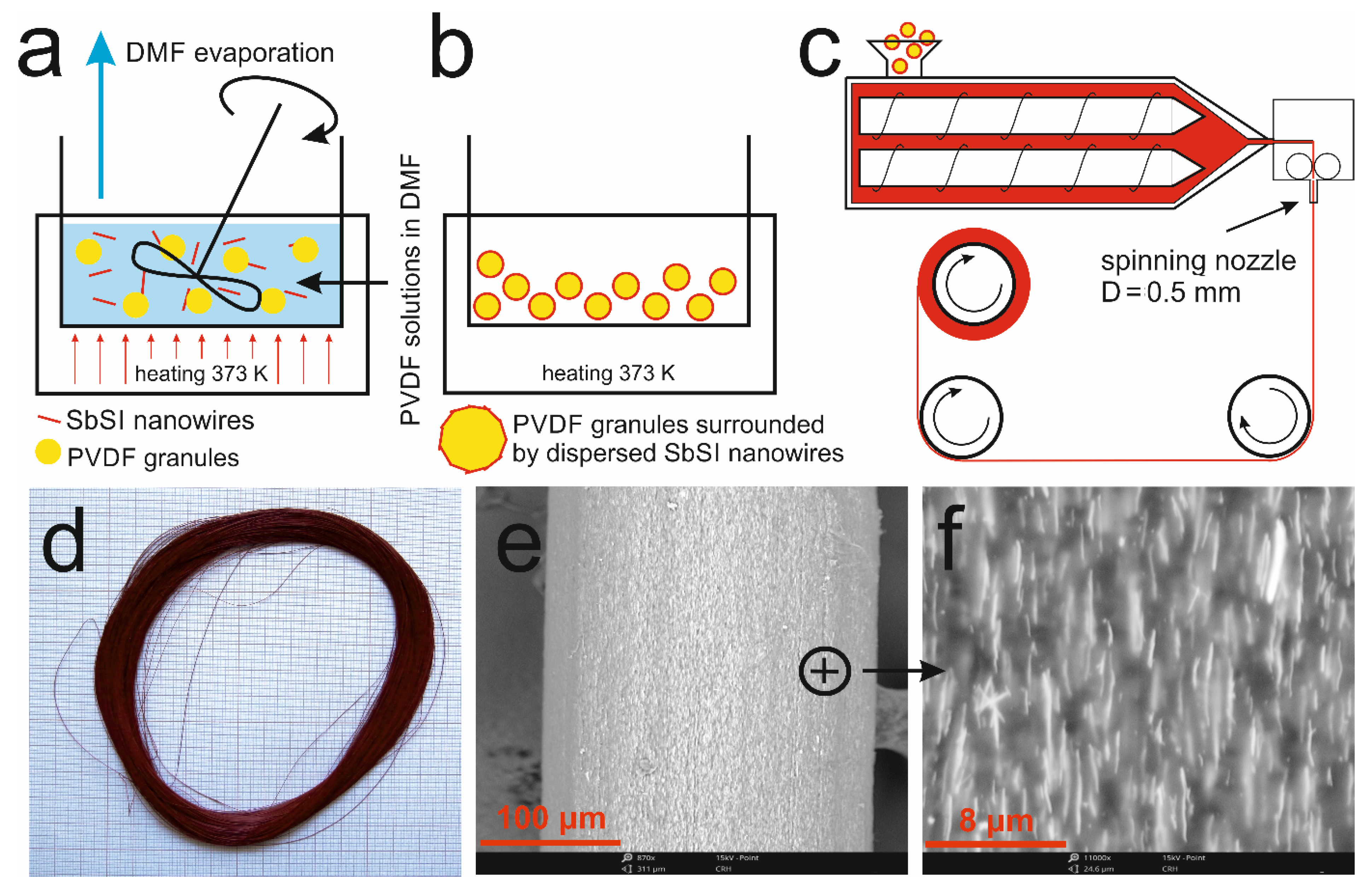
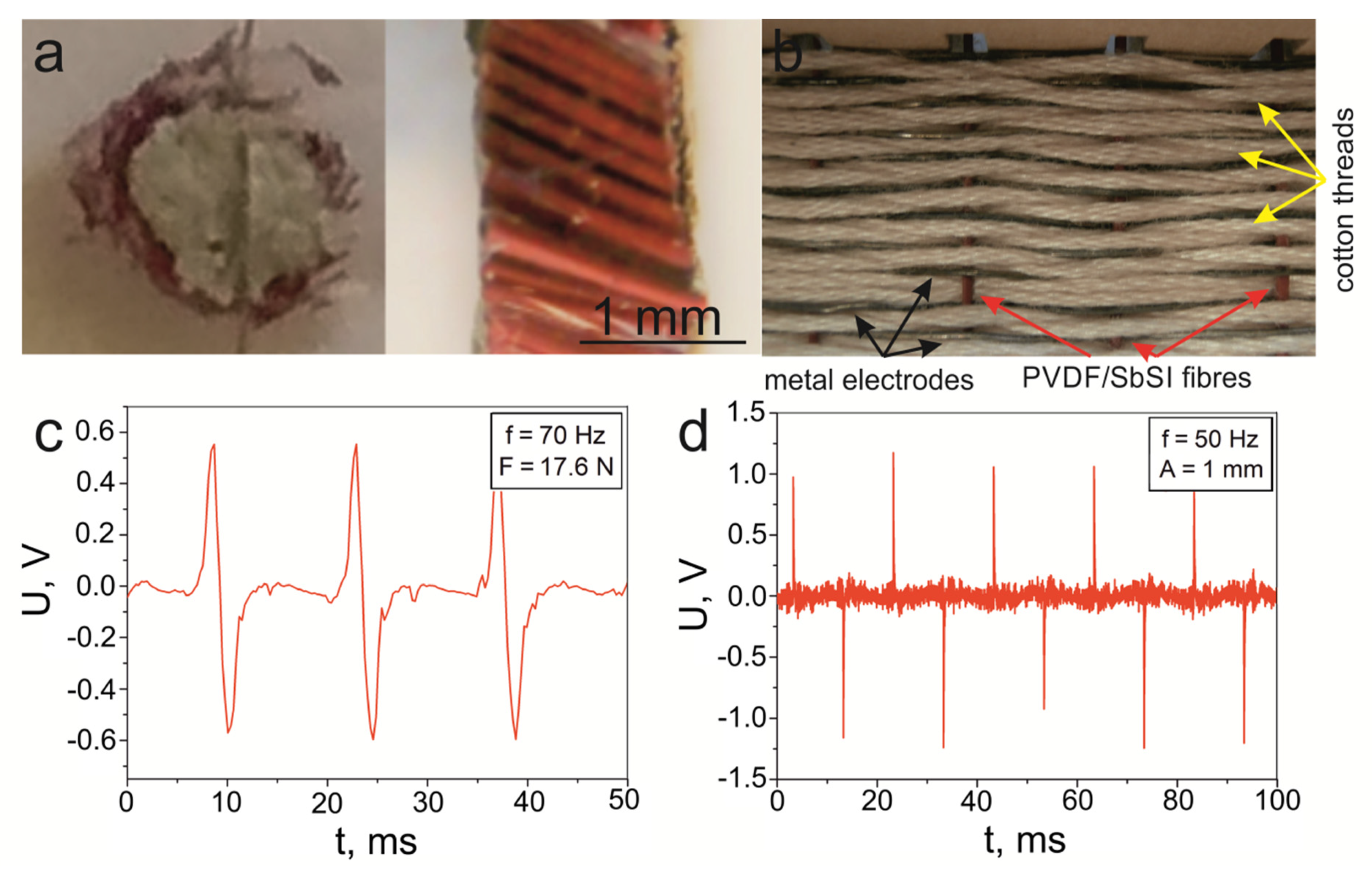
2.5. PVDF/SbSI Composite
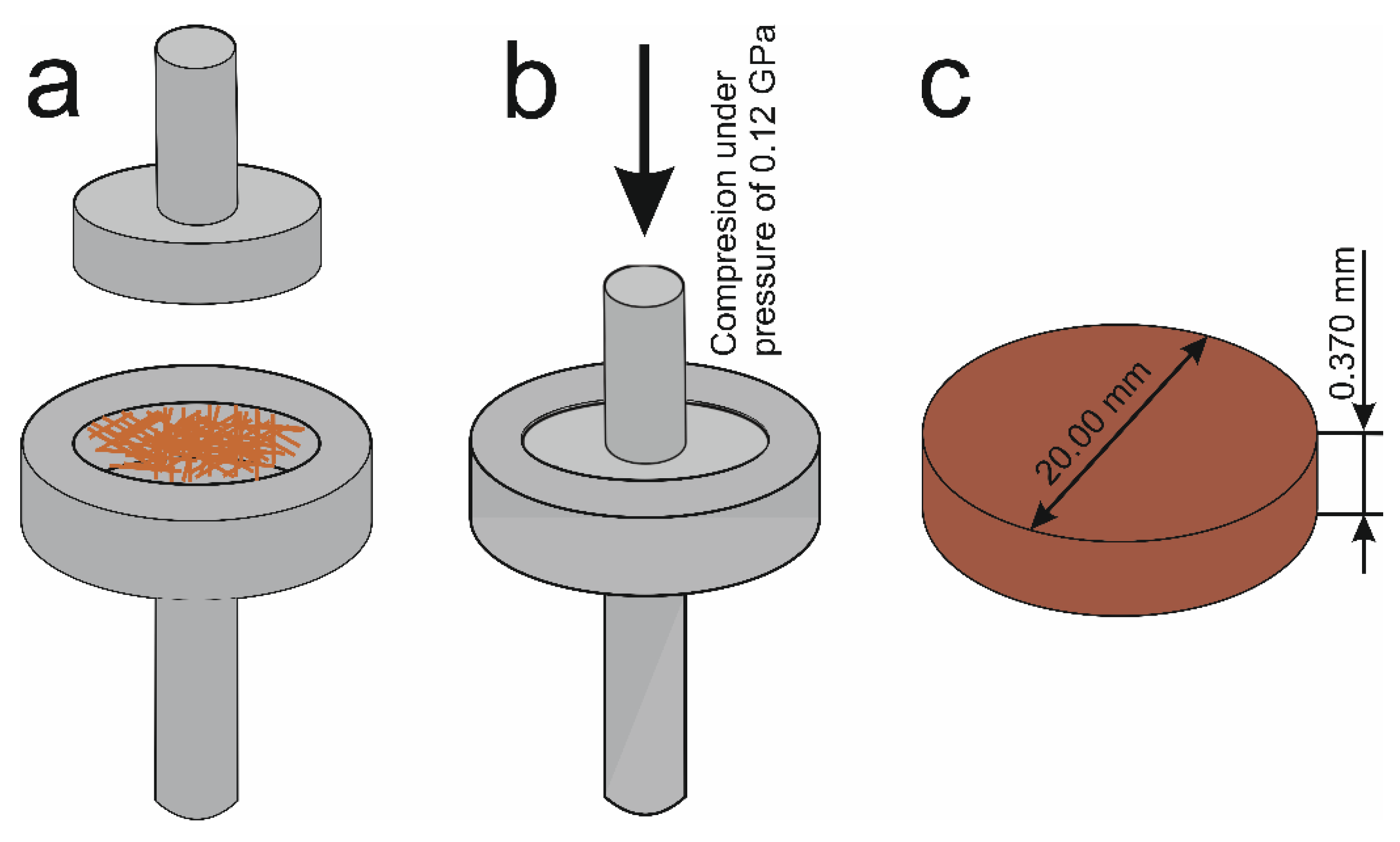
2.6. SbSeI Pellet
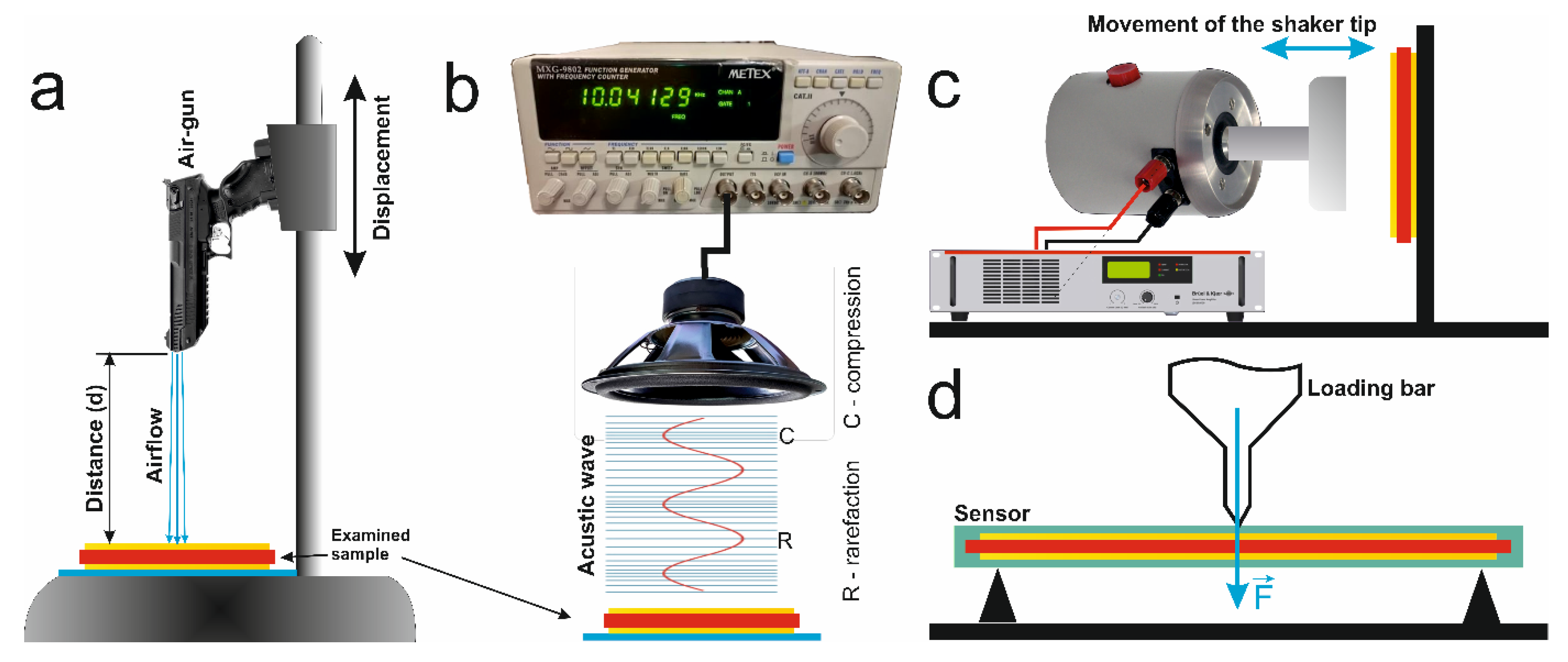
2.7. Measurements
3. Results
3.1. Piezoelectric Nanogenerators
3.2. Pyroelectric Nanogenerators
4. Discussion
5. Conclusions
Funding
Institutional Review Board Statement
Informed Consent Statement
Data Availability Statement
Conflicts of Interest
References
- Wang, Z.L. Self-Powered Nanotech. Sci. Am. 2008, 298, 82–87. [Google Scholar] [CrossRef]
- Wang, Z.L. Piezoelectric nanogenerators based on zinc oxide nanowire arrays. Science 2006, 312, 242–246. [Google Scholar] [CrossRef] [PubMed]
- Yang, Y.; Wang, S.; Zhang, Y.; Wang, Z.L. Supplementary materials: Pyroelectric nanogenerators for driving wireless sensors. Nano Lett. Support. Inf. 2012, 12, 6408–6413. [Google Scholar] [CrossRef] [PubMed] [Green Version]
- Fan, F.R.; Tian, Z.Q.; Lin Wang, Z. Flexible triboelectric generator. Nano Energy 2012, 1, 328–334. [Google Scholar] [CrossRef]
- Kumar, B.; Kim, S.W. Energy harvesting based on semiconducting piezoelectric ZnO nanostructures. Nano Energy 2012, 1, 342–355. [Google Scholar] [CrossRef]
- Zhu, G.; Yang, R.; Wang, S.; Wang, Z.L. Flexible high-output nanogenerator based on lateral ZnO nanowirearray. Nano Lett. 2010, 10, 3151–3155. [Google Scholar] [CrossRef] [PubMed] [Green Version]
- Zhao, Y.; Deng, P.; Nie, Y.; Wang, P.; Zhang, Y.; Xing, L.; Xue, X. Biomolecule-adsorption-dependent piezoelectric output of ZnO nanowire nanogenerator and its application as self-powered active biosensor. Biosens. Bioelectron. 2014, 57, 269–275. [Google Scholar] [CrossRef]
- Lin, Y.F.; Song, J.; Ding, Y.; Lu, S.Y.; Wang, Z.L. Piezoelectric nanogenerator using CdS nanowires. Appl. Phys. Lett. 2008, 92, 23–25. [Google Scholar] [CrossRef]
- Lin, Y.F.; Song, J.; Ding, Y.; Lu, S.Y.; Wang, Z.L. Alternating the output of a CdS nanowire nanogenerator by a white-light-stimulated optoelectronic effect. Adv. Mater. 2008, 20, 3127–3130. [Google Scholar] [CrossRef]
- Chen, X.; Xu, S.; Yao, N.; Shi, Y. 1.6 V nanogenerator for mechanical energy harvesting using PZT nanofibers. Nano Lett. 2010, 10, 2133–2137. [Google Scholar] [CrossRef]
- Park, K.I.; Son, J.H.; Hwang, G.T.; Jeong, C.K.; Ryu, J.; Koo, M.; Choi, I.; Lee, S.H.; Byun, M.; Wang, Z.L.; et al. Highly-efficient flexible piezoelectric PZT thin film nanogenerator on plastic substrates. Adv. Mater. 2014, 26, 2514–2520. [Google Scholar] [CrossRef] [PubMed]
- Cha, S.; Kim, S.M.; Kim, H.; Ku, J.; Sohn, J.I.; Park, Y.J.; Song, B.G.; Jung, M.H.; Lee, E.K.; Choi, B.L.; et al. Porous PVDF as effective sonic wave driven nanogenerators. Nano Lett. 2011, 11, 5142–5147. [Google Scholar] [CrossRef] [PubMed]
- Shin, S.H.; Kim, Y.H.; Lee, M.H.; Jung, J.Y.; Seol, J.H.; Nah, J. Lithium-doped zinc oxide nanowires-polymer composite for high performance flexible piezoelectric nanogenerator. ACS Nano 2014, 8, 10844–10850. [Google Scholar] [CrossRef]
- Zhou, Y.S.; Wang, K.; Han, W.; Rai, S.C.; Zhang, Y.; Ding, Y.; Pan, C.; Zhang, F.; Zhou, W.; Wang, Z.L. Vertically aligned CdSe nanowire arrays for energy harvesting and piezotronic devices. ACS Nano 2012, 6, 6478–6482. [Google Scholar] [CrossRef] [PubMed]
- Xu, H.B.; Lee, T.G.; Park, S.J.; Kim, B.Y.; Nahm, S. Sodium-potassium niobate nanorods with various crystal structures and their application to nanogenerator. J. Am. Ceram. Soc. 2017, 100, 1673–1681. [Google Scholar] [CrossRef]
- Nowak, M.; Szperlich, P.; Bober, Ł.; Szala, J.; Moskal, G.; Stróż, D. Sonochemical preparation of SbSI gel. Ultrason. Sonochem. 2008, 15, 709–716. [Google Scholar] [CrossRef]
- Nowak, M.; Kauch, B.; Szperlich, P.; Jesionek, M.; Kępińska, M.; Bober, Ł.; Szala, J.; Moskal, G.; Rzychoń, T.; Stróż, D. Sonochemical preparation of SbSeI gel. Ultrason. Sonochem. 2009, 16, 546–551. [Google Scholar] [CrossRef]
- Henry. Garot Iode et sulfure d’antimoine. Examen de l’action réciproque de ces deux corps et d’un composé qui en résulte. J. Pharm. 1824, 10, 511–524. [Google Scholar]
- Dönges, E. Über Chalkogenohalogenide des dreiwertigen Antimons und Wismuts.I. Über Thiohalogenide des dreiwertigen Antimons und Wismuts. Z. Anorg. Allg. Chem. 1950, 263, 112–132. [Google Scholar] [CrossRef]
- Dönges, E. Über Chalkogenohalogenide des dreiwertigen Antimons und Wismuts. II. Über Selenohalogenide des dreiwertigen Antimons und Wismuts und über Antimon(III)–selenid Mit 2 Abbildungen. Z. Anorg. Allg. Chem. 1950, 263, 280–291. [Google Scholar] [CrossRef]
- Nitsche, R.; Merz, W.J. Photoconduction in ternary V–VI–VII compounds. J. Phys. Chem. Solid 1960, 13, 154–155. [Google Scholar] [CrossRef]
- Fatuzzo, E.; Harbeke, G.; Merz, W.J.; Nitsche, R.; Roetschi, H.; Ruppel, W. Ferroelectricity in SbSI. Phys. Rev. 1962, 127, 2036–2037. [Google Scholar] [CrossRef]
- Fridkin, V.M.; Rodin, A.I. Anomalous photovoltaic effect in ferroelectric SbSI and cubic piezoelectric ZnS. Phys. Status Solidi A 1980, 61, 123–126. [Google Scholar] [CrossRef]
- Akopov, D.R.; Grekov, A.A.; Rodin, A.I. Anomalous photovoltaic effect in AVBVICVII ferroelectrics. Ferroelectrics 1980, 26, 855–858. [Google Scholar] [CrossRef]
- Nakamura, M.; Horiuchi, S.; Kagawa, F.; Ogawa, N.; Kurumaji, T.; Tokura, Y.; Kawasaki, M. Shift current photovoltaic effect in a ferroelectric charge-transfer complex. Nat. Commun. 2017, 8, 281. [Google Scholar] [CrossRef]
- Ogawa, N.; Sotome, M.; Kaneko, Y.; Ogino, M.; Tokura, Y. Shift current in the ferro-electric semiconductor SbSI. Phys. Rev. B 2017, 96, 241203I. [Google Scholar] [CrossRef] [Green Version]
- Nakamura, M.; Hatada, H.; Kaneko, Y.; Ogawa, N.; Tokura, Y.; Kawasaki, M. Impact of electrodes on the extraction of shift current from a ferroelectric semiconductor SbSI. Appl. Phys. Lett. 2018, 113, 232901. [Google Scholar] [CrossRef]
- Sotome, M.; Nakamuraa, M.; Fujioka, J.; Ogino, M.; Kaneko, Y.; Morimotod, T.; Zhange, Y.; Kawasakia, M.; Nagaosa, N.; Tokuraa, Y.; et al. Spectral dynamics of shift current in ferroelectric semiconductor SbSI. Proc. Natl. Acad. Sci. USA 2019, 116, 1929–1933. [Google Scholar] [CrossRef] [Green Version]
- Burger, A.M.; Agarwal, R.; Aprelev, A.; Schruba, E.; Gutierrez-Perez, A.; Fridkin, V.M.; Spanier, J.E. Direct observation of shift and ballistic photovoltaic currents. Sci. Adv. 2019, 5, eaau5588. [Google Scholar] [CrossRef] [Green Version]
- Teng, M.K.; Balkanski, M.; Massot, M. Soft-photon couplings in the pressure-induced phase transition in SbSI. Phys. Rev. B 1971, 5, 1031–1034. [Google Scholar] [CrossRef]
- Popolitov, V.I. Synthesis of triple chalcogenides AVBVICVII with the perovskite structure. Kristallografiya 1969, 14, 375–376. [Google Scholar]
- Sereika, R.; Žaltauskas, R.; Lapeika, V.; Stanionytė, S.; Juškėnas, R. Structural changes in chlorine-substituted SbSI. J. Appl. Phys. 2019, 126, 114101. [Google Scholar] [CrossRef]
- Berlincourt, D.; Jaffe, H.; Merz, J.W.; Nitsche, R. Piezoelectric effect in the ferroelectric range in SbSI. Appl. Phys. Lett. 1964, 4, 61–63. [Google Scholar] [CrossRef]
- Mori, T.; Tamura, H. Preparation of ferroelectric SbSI single crystals. J. Phys. Soc. Jpn. 1964, 19, 1247. [Google Scholar] [CrossRef]
- Grigas, J.; Kajokas, A.; Audzijonis, A.; Zigas, L. Peculiarities and properties of SbSI electroceramics. J. Eur. Ceram. Soc. 2001, 21, 1337–1340. [Google Scholar] [CrossRef]
- Talarczyk, E. Podstawy Techniki Ultradźwięków; Politechnika Wrocławska: Wrocław, Poland, 1990. [Google Scholar]
- Jordan, T.; Ounaies, Z. Characterization of Piezoelectric Ceramic Materials. In Encyclopedia of Smart Materials; Schwartz, M., Ed.; Wiley: New York, NY, USA, 2002. [Google Scholar]
- Perls, T.A.; Diesel, T.; Dobrow, W.I. Primary pyroelectricity in barium titanate ceramics. J. Appl. Phys. 1958, 29, 1297–1302. [Google Scholar] [CrossRef]
- Schaefer, A.; Schmitt, H.; Dorr, A. Elastic and piezoelectric coefficients of TSSG barium titanate single crystals. Ferroelectrics 1986, 69, 253–266. [Google Scholar] [CrossRef]
- Shiosaki, T.; Lian, J.; Adachi, M.; Kawabata, A. Pyroelectric and ferroelectric properties in the PZT-Pb(Zn1/3Nb2/3)O3 system. Ferroelectrics 1989, 92, 23–28. [Google Scholar] [CrossRef]
- Czekaj, D.; Surowiak, Z.; Bakirov, A.A.; Dudkievich, V.P. Piezoelectric effect in RF sputtered ferroelectric thin films. J. Eur. Ceram. Soc. 2001, 21, 1609–1613. [Google Scholar] [CrossRef]
- Topolov, V.Y.; Turik, A.V.; Chernobabov, A.I. Evaluation of nontrivial behaviour of electromechanical coupling factors in PbTiO3-type ferroelectric ceramics. J. Eur. Ceram. Soc. 1999, 19, 1213–1217. [Google Scholar] [CrossRef]
- Sasaki, Y. Photoconductivity of ferroelectric photoconductor SbSI. Jpn. J. Appl. Phys. 1964, 3, 558–559. [Google Scholar] [CrossRef]
- Hamano, K.; Nakamura, T.; Ishibashi, Y.; Ooyane, T. Piezoelectric property of SbSI single crystal. J. Phys. Soc. Jpn. 1965, 20, 1886–1888. [Google Scholar] [CrossRef]
- Molnar, B.; Johannes, R.; Haas, E. Properties of single-crystal SbSI. Bull. Amer. Phys. Soc. 1965, 10, 109. [Google Scholar]
- Ishikawa, K.; Shikata, Y.; Toyoda, K. Dielectric properties of Sb1-xBixSI crystals. Phys. Stat. Sol. A 1974, 25, 187–189. [Google Scholar] [CrossRef]
- Kikuchi, A.; Oka, Y.; Sawaguchi, E. Crystal structure determination of SbSI. J. Phys. Soc. Jpn. 1967, 23, 337–354. [Google Scholar] [CrossRef]
- Dziuba, Z. Crystallization of SbSI crystal from the vapour phase. J. Cryst. Growth 1976, 35, 340–342. [Google Scholar] [CrossRef]
- Zadorozhnaya, L.A.; Lyachovitskaya, V.A.; Givargizov, E.I.; Belyaev, L.M. Vapour growth of SbSI on a seed. J. Cryst. Growth 1977, 41, 61–66. [Google Scholar] [CrossRef]
- Łukaszewicz, K.; Pietraszko, A.; Stępień-Damm, J.; Kajokas, J. Crystal structure and phase transitions of the ferroelectric antimony sulfoiodide SbSI. Part II. Crystal structure of SbSI in phases I, II and II. Pol. J. Chem. 1997, 71, 1852–1857. [Google Scholar]
- Szperlich, P.; Toroń, B.; Nowak, M.; Jesionek, M.; Kępińska, M.; Bogdanowicz, W. Growth of large SbSI crystals. Mater. Sci. Pol. 2014, 32, 669–675. [Google Scholar] [CrossRef] [Green Version]
- Mori, T.; Tamura, H. Specific heat measurement of ferroelectric SbSI. J. Phys. Soc. Jpn. 1965, 20, 281. [Google Scholar] [CrossRef]
- Nitsche, R.; Roetschi, H.; Wild, P. New ferroelectric V-VI-VII compounds of the SbSI type. Appl. Phys. Lett. 1964, 4, 210–211. [Google Scholar] [CrossRef]
- Masuda, Y.; Sakata, K.; Hasegawa, S.; Ohara, G.; Wada, M. Growth and some electrical properties of orientated crystal of SbSI. Jap. J. Appl. Phys. 1969, 8, 692–699. [Google Scholar] [CrossRef]
- Nassau, K.; Shiever, J.W.; Kowalchik, M. The growth of large SbSI crystals: Control of needle morphology. J. Cryst. Growth 1970, 7, 237–245. [Google Scholar] [CrossRef]
- Robertson, D.S. A study of the flow patterns in liquids using a model Czochralski crystal growing system. Br. J. Appl. Phys. 1966, 17, 1047–1051. [Google Scholar] [CrossRef]
- Bhalla, A.S.; Spear, K.E.; Cross, L.E. Crystal growth of antimony sulphur iodide. Mat. Res. Bull. 1979, 14, 423–429. [Google Scholar] [CrossRef]
- Isaac, J.; Philip, J. Temperature dependence of the absorption edge in the ferroelectric phase of SbSI using photoacoustic technique. Phys. Status Solidi B 1991, 165, K47–K50. [Google Scholar] [CrossRef]
- Youn, H.S.; Kim, Y.G.; Kim, H.G.; Kim, W.T.; Kwun, S.I. Impurity optical absorption of SbSI: Ni single crystals. Solid State Comm. 1989, 69, 1195–1196. [Google Scholar] [CrossRef]
- Hyun, S.C.; Kim, Y.G.; Kim, M.Y.; Koh, J.D.; Park, B.S.; Kim, W.T. Optical properties of undoped and chromium-doped VA-VIA-VIIA single crystals. J. Mater. Sci. 1995, 30, 6113–6117. [Google Scholar] [CrossRef]
- Neels, H.; Schmitz, W.; Hottmann, H.; Roessner, R.; Topp, W. On the crystallization process of SbSI with special reference to the oscillation method. Krist. Und Tech. 1971, 6, 225–243. [Google Scholar] [CrossRef]
- Porat, Y.; Ting, R.Y. The piezoelectric and dielectric properties of SbSi(Sb2S3) x composites. Ferroelectrics 1988, 87, 155–165. [Google Scholar] [CrossRef]
- Boksha, S.S. High gas pressure crystal growth of antimony sulpho-iodide, nickel carbonate and black phosphorus. J. Cryst. Growth 1972, 12, 113–119. [Google Scholar] [CrossRef]
- Okazaki, K.; Narushima, S.J. Electrical properties of the hot-pressed SbSI polycrystals. J. Ceram. Soc. Jpn. 1968, 76, 21–27. [Google Scholar] [CrossRef] [Green Version]
- Lefkowitz, I.; Brodman, B.; Radell, J.; Shieldsm, M. Preparation, crystal optics, X-ray diffraction and electrical studies of antimony sufide iodide. Bull. Am. Phys. Soc. 1965, 10, 617. [Google Scholar]
- Wang, C.; Tang, K.; Yang, Q.; Hai, B.; Shen, G.; An, C.; Yu, W.; Qian, Y. Synthesis of novel SbSI nanorods by a hydrothermal method. Inorg. Chem. Commun. 2001, 4, 339–341. [Google Scholar] [CrossRef]
- Yang, Q.; Tang, K.; Wang, C.; Hai, B.; Shen, G.; An, C.; Zhang, C.; Qian, Y. The synthesis of SbSI rodlike crystals with studded pyramids. J. Cryst. Growth 2001, 233, 774–778. [Google Scholar] [CrossRef]
- Okazaki, K. ISAF’96 Proceedings of the 10th IEEE International Symposium on Applications of Ferroelectrics; IEEE: Piscataway, NJ, USA, 1996; Volume 2, pp. 779–782. [Google Scholar]
- Mistewicz, K.; Nowak, M.; Paszkiewicz, R.; Guiseppi-Elie, A. SbSI Nanosensors: From gel to single nanowire devices. Nanoscale Res. Lett. 2017, 12, 97. [Google Scholar] [CrossRef] [Green Version]
- Szperlich, P.; Nowak, M.; Bober, Ł.; Szala, J.; Stróż, D. Ferroelectric properties of ultrasonochemically prepared SbSI ethanogel. Ultrason. Sonochem. 2009, 16, 398–401. [Google Scholar] [CrossRef]
- Nowak, M.; Kauch, B.; Szperlich, P. Determination of energy band gap of nanocrystalline SbSI using diffuse reflectance spectroscopy. Rev. Sci. Instrum. 2009, 80, 046107. [Google Scholar] [CrossRef]
- Nowak, M.; Talik, E.; Szperlich, P.; Stróż, D. XPS analysis of sonochemically prepared SbSI ethanogel. Appl. Surf. Sci. 2009, 255, 7689–7694. [Google Scholar] [CrossRef]
- Starczewska, A.; Nowak, M.; Szperlich, P.; Toroń, B.; Mistewicz, K.; Stróż, D.; Szala, J. Influence of humidity on impedance of SbSI gel. Sens. Actuator A Phys. 2012, 183, 34–42. [Google Scholar] [CrossRef]
- Nowak, M.; Szperlich, P. Temperature dependence of energy band gap and spontaneous polarization of SbSI nanowires. Opt. Mater. 2013, 35, 1200–1206. [Google Scholar] [CrossRef]
- Nowak, M.; Bober, Ł.; Borkowski, B.; Kępińska, M.; Szperlich, P.; Stróż, D.; Sozańska, M. Quantum efficiency coefficient for photogeneration of carriers in SbSI nanowires. Opt. Mater. 2013, 35, 2208–2216. [Google Scholar] [CrossRef]
- Mistewicz, K.; Nowak, M.; Wrzalik, R.; Jesionek, M.; Szperlich, P.; Paszkiewicz, R.; Guiseppi-Elie, A. Quantum effects in conductivity and photoconductivity of a single SbSI nanowire. Acta Phys. Pol. A 2013, 124, 827–829. [Google Scholar] [CrossRef]
- Starczewska, A.; Wrzalik, R.; Nowak, M.; Szperlich, P.; Jesionek, M.; Moskal, G.; Rzychoń, T.; Szala, J.; Stróż, D.; Maślanka, P. Influence of the solvent on ultrasonically produced SbSI nanowires. Ultrason. Sonochem. 2009, 16, 537–545. [Google Scholar] [CrossRef]
- Tasviri, M.; Sajadi-Hezave, Z. SbSI nanowires and CNTs encapsulated with SbSI as photocatalysts with high visible-light driven photoactivity. Mol. Catal. 2017, 436, 174–181. [Google Scholar] [CrossRef]
- Kwolek, P.; Pilarczyk, K.; Tokarski, T.; Mech, J.; Irzmański, J.; Szaciłowski, K. Photoelectrochemistry of n-type antimony sulfoiodide nanowires. Nanotechnology 2015, 26, 105710. [Google Scholar] [CrossRef]
- Nowak, M.; Nowrot, A.; Szperlich, P.; Jesionek, M.; Kȩpińska, M.; Starczewska, A.; Mistewicz, K.; Stróz, D.; Szala, J.; Rzychoń, T.; et al. Fabrication and characterization of SbSI gel for humidity sensors. Sens. Actuator A Phys. 2014, 210, 119–130. [Google Scholar] [CrossRef]
- Szperlich, P.; Nowak, M.; Jesionek, M.; Starczewska, A.; Mistewicz, K.; Szala, J. Desorption of Gasses Induced by Ferroelectric Transition in SbSI Nanowires. Acta Phys. Pol. A 2014, 126, 1110–1112. [Google Scholar] [CrossRef]
- Gladkovskaya, O.; Rybina, I.; Gunko, Y.K.; Erxleben, A.; O’Connor, G.M.; Rochev, Y. Water-based ultrasonic synthesis of SbSI nanoneedles. Mater. Lett. 2015, 160, 113–116. [Google Scholar] [CrossRef]
- Nowak, M.; Tański, T.; Szperlich, P.; Matysiak, W.; Kępińska, M.; Stróż, D.; Bober, Ł.; Toroń, B. Using of sonochemically prepared SbSI for electrospun nanofibers. Ultrason. Sonochem. 2017, 38, 544–552. [Google Scholar] [CrossRef]
- Nowak, M.; Kauch, B.; Szperlich, P.; Stróż, D.; Szala, J.; Rzychon, T.; Bober, Ł.; Toroń, B.; Nowrot, A. Sonochemical preparation of SbS1xSexI nanowires. Ultrason. Sonochem. 2010, 17, 487–493. [Google Scholar] [CrossRef]
- Suslick, K.S.; Hammerton, D.A.; Cline, R.E. The sonochemical Hot Spot. J. Am. Chem. Soc. 1986, 108, 5641–5642. [Google Scholar] [CrossRef]
- Lupeiko, T.G.; Lopatin, S.S. Old and new problems in piezoelectric materials research and materials with high hydrostatic sensitivity. Inorg. Mater. 2004, 40 (Suppl. S1), S19–S32. [Google Scholar] [CrossRef]
- Nan, C.W.; Jia, Q. Obtaining ultimate functionalities in nanocomposites: Design, control, and fabrication. MRS Bull. 2015, 40, 719–724. [Google Scholar] [CrossRef] [Green Version]
- Toron, B.; Szperlich, P.; Nowak, M.; Stróż, D.; Rzychoń, T. Novel piezoelectric paper based on SbSI nanowires. Cellulose 2018, 25, 7–15. [Google Scholar] [CrossRef] [Green Version]
- Szperlich, P.; Toroń, B. An ultrasonic fabrication method for epoxy resin/SbSI nanowire composites, and their application in nanosensors and nanogenerators. Polymers 2019, 11, 479. [Google Scholar] [CrossRef] [Green Version]
- Kozioł, M.; Toroń, B.; Szperlich, P.; Jesionek, M. Fabrication of a piezoelectric strain sensor based on SbSI nanowires as a structural element of a FRP laminate. Compos. Part B 2019, 157, 58–65. [Google Scholar] [CrossRef]
- Kozioł, M.; Szperlich, P.; Toroń, B.; Olesik, P.; Jesionek, M. Assessment of the piezoelectric response of an epoxy resin/SbSI nanowires composite filling FDM printed grid. Materials 2020, 13, 5281. [Google Scholar] [CrossRef]
- Jesionek, M.; Toroń, B.; Szperlich, P.; Biniaś, W.; Biniaś, D.; Rabiej, S.; Starczewska, A.; Nowak, M.; Kępińska, M.; Dec, J. Fabrication of a new PVDF/SbSI nanowire composite for smart wearable textile. Polymer 2019, 180, 121729. [Google Scholar] [CrossRef]
- Mistewicz, K.; Nowak, M.; Stróż, D.; Paszkiewicz, R. SbSI nanowires for ferroelectric generators operating under shock pressure. Mater. Lett. 2016, 180, 15–18. [Google Scholar] [CrossRef]
- Mistewicz, K.; Nowak, M.; Wrzalik, R.; Śleziona, J.; Wieczorek, K.; Guiseppi-Elie, A. Ultrasonic processing of SbSI nanowires for their application to gas sensors. Ultrasonics 2016, 69, 67–73. [Google Scholar] [CrossRef] [PubMed]
- Toroń, B.; Mistewicz, K.; Jesionek, M.; Kozioł, M.; Stróż, D.; Zubko, M. Nanogenerator for dynamic stimuli detection and mechanical energy harvesting based on compressed SbSeI nanowires. Energy 2020, 212, 118717. [Google Scholar] [CrossRef]
- Mistewicz, K.; Jesionek, M.; Nowak, M.; Kozioł, M. SbSeI pyroelectric nanogenerator for a low temperature waste heat recovery. Nano Energy 2019, 64, 103906. [Google Scholar] [CrossRef]
- California Institute of Technology. Brief History of Thermoelectrics. 2017. Available online: http://www.thermoelectrics.caltech.edu/thermoelectrics/history.html (accessed on 10 November 2017).
- SN Systems. Thermionic Energy Conversion. 2017. Available online: https://nems.stanford.edu/thermionic-energy-conversion (accessed on 3 November 2017).
- Caillat, T.; Fleurial, J.-P.; Snyder, G.J.; Zoltan, A.; Zoltan, D.; Borshchevsky, A. A new high efficiency segmented thermoelectric unicouple. In Proceedings of the 34th Intersociety Energy Conversion Engineering Conference 1999, Vancouver, BC, Canada, 2–5 August 1999; p. 2567. [Google Scholar]
- Jouhara, H.; Khordehgah, N.; Almahmoud, S.; Delpech, B.; Chauhan, A.; Tassou, S.A. Waste heat recovery technologies and applications. Therm. Sci. Eng. Prog. 2018, 6, 268–289. [Google Scholar] [CrossRef]
- Kishore, R.A.; Priya, S. A review on low-grade thermal energy harvesting: Materials, methods and devices. Materials 2018, 11, 1433. [Google Scholar] [CrossRef] [Green Version]
- Toroń, B.; Szperlich, P.; Nowak, M.; Matysiak, W.; Tański, T.; Starczewska, A. A new estimation method of piezoelectric coefficient based on pressure shock wave. Appl. Mat. Lett. submitted.
- Bhalla, A.S.; Newnham, R.E.; Shrout, T.R.; Cross, L.E. Piezoelectric SbSI:polymer composites. Ferroelectrics 1982, 41, 207–211. [Google Scholar] [CrossRef]
- Zhang, L.; Zhang, F.; Qin, Z.; Han, Q.; Wang, T.; Chu, F. Piezoelectric energy harvester for rolling bearings with capability of self-powered condition monitoring. Energy 2022, 238, 121770. [Google Scholar] [CrossRef]
- Rozylo, P. A study of failure analysis of composite profile with open cross-section under axial compression. Compos. Theory Pract. 2018, 18, 210–216. [Google Scholar]
- Horoschenkoff, A.; Klein, S.; Haase, K.-H. Structural Integration of Strain Gages; Hottinger Baldwin Messtechnik GmbH: Darmstadt, Germany, 2006. [Google Scholar]
- Dragan, K.; Dziendzikowski, M.; Leski, A. Self-diagnostics of composite aerospace structures with use of intelligent materials. Prz. Spaw. 2015, 87, 41–44. [Google Scholar]
- Zhang, Q.; Agbossou, A.; Feng, Z.; Cosnier, M. Solar micro-energy harvesting with pyroelectric effect and wind flow. Sens. Actuators A 2011, 168, 335–342. [Google Scholar] [CrossRef]
- Siao, A.-S.; Chao, C.-H.; Hsiao, C.-C. Study on pyroelectric harvesters with various Geometry. Sensors 2015, 15, 19633–19648. [Google Scholar] [CrossRef] [PubMed] [Green Version]
- Zhang, K.; Wang, Y.; Wang, Z.L.; Yang, Y. Standard and figure-of-merit for quantifying the performance of pyroelectric nanogenerators. Nano Energy 2019, 55, 534–540. [Google Scholar] [CrossRef]
- Raghavendra, R.M.; Praneeth, K.P.S.S.; Dutta, S. Preparation and characterization of BaTiO3–PbZrTiO3 coating for pyroelectric energy harvesting. J. Electron. Mater. 2017, 46, 101–106. [Google Scholar] [CrossRef]
- Tabbai, Y.; Belhora, F.; El Moznine, R.; Hajjaji, A.; El Ballouti, A. Pyroelectric effect in lead zirconate titanate/polyurethane composite for thermal energy harvesting. Eur. Phys. J. Appl. Phys. 2019, 86, 10902. [Google Scholar] [CrossRef]
- Bhalla, A.S.; Newnham, R.E.; Cross, L.E.; Dougherty, J.P.; Smith, W.A. Pyroelectricity in SbSI. Ferroelectrics 1981, 33, 3–7. [Google Scholar] [CrossRef]
- Lee, J.; Min, B.-K.; Cho, I.; Sohn, Y. Synthesis and characterization of 1-D BiSI and 2-D BiOI nanostructures. Bull. Korean Chem. Soc. 2013, 34, 773–777. [Google Scholar] [CrossRef] [Green Version]
- Toroń, B.; Nowak, M.; Kępińska, M.; Grabowski, A.; Szala, J.; Szperlich, P.; Mala, I.; Rzychoń, T. A new heterostructures fabrication technique and properties of produced SbSI/Sb2S3 heterostructures. Opt. Lasers Eng. 2014, 55, 232–236. [Google Scholar] [CrossRef]
- Lee, M.; Chen, C.Y.; Wang, S.; Cha, S.N.; Park, Y.J.; Kim, J.M.; Chou, L.J.; Wang, Z.L. A hybrid piezoelectric structure for wearable nanogenerators. Adv. Mater. 2012, 24, 1759–1764. [Google Scholar] [CrossRef]
- Liang, L.; Kang, X.; Sang, Y.; Liu, H. One-dimensional ferroelectric nanostructures: Synthesis, properties, and applications. Adv. Sci. 2016, 3, 1500358. [Google Scholar] [CrossRef] [Green Version]
- Purusothaman, Y.; Alluri, N.R.; Chandrasekhar, A.; Kim, S.-J. Photoactive piezoelectric energy harvester driven by antimony sulfoiodide (SbSI): A AVBVICVII class ferroelectric-semiconductor compound. Nano Energy 2018, 50, 256–265. [Google Scholar] [CrossRef]
- Chang, C.; Tran, V.H.; Wang, J.; Fuh, Y.-K.; Lin, L. Direct-write piezoelectric polymeric nanogenerator with high energy conversion efficiency. Nano Lett. 2010, 10, 726–731. [Google Scholar] [CrossRef] [PubMed]
- Zhang, G.; Liao, Q.; Zhang, Z.; Liang, Q.; Zhao, Y.; Zheng, X.; Zhang, Y. Novel piezoelectric paper based flexible nanogenerators composed of BaTiO3 nanoparticles and bacterial cellulose. Adv. Sci. 2016, 3, 1500257. [Google Scholar] [CrossRef] [PubMed]
- Starr, M.B.; Wang, X. Coupling of piezoelectric effect with electrochemical processes. Nano Energy 2015, 14, 296–311. [Google Scholar] [CrossRef] [Green Version]
- Starr, M.B.; Wang, X. Fundamental analysis of piezocatalysis process on the surfaces of strained piezoelectric materials. Sci. Rep. 2013, 3, 2160. [Google Scholar] [CrossRef] [Green Version]
- Starr, M.B.; Shi, J.; Wang, X. Piezopotential-driven redox reactions at the surface of piezoelectric materials. Angew. Chem. Int. Ed. 2012, 51, 5962–5966. [Google Scholar] [CrossRef] [PubMed]
- Pan, L.; Sun, S.; Chen, Y.; Wang, P.; Wang, J.; Zhang, X.; Zou, J.-J.; Wang, Z.L. Advances in piezo-phototronic effect enhanced photocatalysis and photoelectrocatalysis. Adv. Energy Mater. 2020, 10, 2000214. [Google Scholar] [CrossRef]
- Liang, Z.; Yan, C.-F.; Rtimi, S.; Bandara, J. Piezoelectric materials for catalytic/photocatalytic removal of pollutants: Recent advances and outlook. Appl. Catal. B Environ. 2019, 241, 256–269. [Google Scholar] [CrossRef]
- Li, S.; Zhao, Z.; Zhao, J.; Zhang, Z.; Li, X.; Zhang, J. Recent advances of ferro-, piezo-, and pyroelectric nanomaterials for catalytic applications. ACS Appl. Nano Mater. 2020, 3, 1063–1079. [Google Scholar] [CrossRef]
- Wu, J.; Qin, N.; Bao, D. Effective enhancement of piezocatalytic activity of BaTiO3 nanowires under ultrasonic vibration. Nano Energy 2018, 45, 44–51. [Google Scholar] [CrossRef]
- Merouani, S.; Hamdaoui, O.; Rezgui, Y.; Guemini, M. Theoretical estimation of the temperature and pressure within collapsing acoustical bubbles. Ultrason. Sonochem. 2014, 21, 53–59. [Google Scholar] [CrossRef] [PubMed]
- Gao, Y.; Wang, Z.L. Electrostatic potential in a bent piezoelectric nanowire. The fundamental theory of nanogenerator and nanopiezotronics. Nano Lett. 2007, 7, 2499–2505. [Google Scholar] [CrossRef] [PubMed]
- Economou, E.N. The Physics of Solids: Essentials and Beyond; Springer: New York, NY, USA, 2010. [Google Scholar]
- Gao, Y.; Wang, Z.L. Equilibrium potential of free charge carriers in a bent piezoelectric semiconductive nanowire. Nano Lett. 2009, 79, 1103–1110. [Google Scholar] [CrossRef] [PubMed]
- Lan, S.; Feng, J.; Xiong, Y.; Tian, S.; Liu, S.; Kong, L. Performance and mechanism of piezocatalytic degradation of 4-chlorophenol: Finding of effective piezo-dechlorination. Environ. Sci. Technol. 2017, 51, 6560–6569. [Google Scholar] [CrossRef]
- Lan, S.; Chen, Y.; Zeng, L.; Ji, H.; Liu, W.; Zhu, M. Piezo-activation of peroxymonosulfate for benzothiazole removal in water. J. Hazard. Mater. 2020, 393, 122448. [Google Scholar] [CrossRef]
- Mistewicz, K.; Kepińska, M.; Nowak, M.; Sasiela, A.; Zubko, M.; Stróż, D. Fast and efficient piezo/photocatalytic removal of methyl orange using SbSI nanowires. Materials 2020, 12, 4803. [Google Scholar] [CrossRef]
- Wu, M.-H.; Lee, J.-T.; Chung, Y.J.; Srinivaas, M.; Wu, J.-M. Ultrahigh efficient degradation activity of single- and few-layered MoSe2 nanoflowers in dark by piezo-catalyst effect. Nano Energy 2017, 40, 369–375. [Google Scholar] [CrossRef]
- Wu, J.M.; Chang, W.E.; Chang, Y.T.; Chang, C.-K. Piezo-catalytic effect on the enhancement of the ultra-high degradation activity in the dark by single- and few-layers MoS2 nanoflowers. CK Adv. Mater. 2016, 28, 3718. [Google Scholar] [CrossRef]
- Masimukku, S.; Hu, Y.C.; Lin, Z.H.; Chan, S.W.; Chou, T.M.; Wu, J.M. High efficient degradation of dye molecules by PDMS embedded abundant single-layer tungsten disulfide and their antibacterial performance. Nano Energy 2018, 46, 338–346. [Google Scholar] [CrossRef]
- Li, H.; Sang, Y.; Chang, S.; Huang, X.; Zhang, Y.; Yang, R.; Jiang, H.; Liu, H.; Wang, Z.L. Enhanced ferroelectric-nanocrystal-based hybrid photocatalysis by ultrasonic-wave-generated piezophototronic effect. Nano Lett. 2015, 15, 2372–2379. [Google Scholar] [CrossRef]
- Xu, S.; Guo, L.; Sun, Q.; Wang, Z.L. Piezotronic effect enhanced plasmonic photocatalysis by AuNPs/BaTiO3 heterostructures. Adv. Funct. Mater. 2019, 29, 1808737. [Google Scholar] [CrossRef]
- Guo, L.; Zhong, C.; Cao, J.; Hao, Y.; Lei, M.; Bi, K.; Sun, Q.; Wang, Z.L. Enhanced photocatalytic H2 evolution by plasmonic and piezotronic effects based on periodic Al/BaTiO3 heterostructures. Nano Energy 2019, 62, 513–520. [Google Scholar] [CrossRef]
- Hong, D.; Zang, W.; Guo, X.; Fu, Y.; He, H.; Sun, J.; Xing, L.; Liu, B.; Xue, X. High piezo-photocatalytic efficiency of CuS/ZnO nanowires using both solar and mechanical energy for degrading organic dye. ACS Appl. Mater. Interfaces 2016, 8, 21302–21314. [Google Scholar] [CrossRef] [PubMed]
- Xue, X.; Zang, W.; Deng, P.; Wang, Q.; Xing, L.; Zhang, Y.; Wang, Z.L. Piezo-potential enhanced photocatalytic degradation of organic dye using ZnO nanowires. Nano Energy 2015, 13, 414–422. [Google Scholar] [CrossRef]
- Feng, Y.; Li, H.; Ling, L.; Yan, S.; Pan, D.; Ge, H.; Li, H.; Bian, Z. Enhanced photocatalytic degradation performance by fluid-induced piezoelectric field. Environ. Sci. Technol. 2018, 52, 7842–7848. [Google Scholar] [CrossRef] [PubMed]
- Ma, J.; Ren, J.; Jia, Y.; Wu, Z.; Chen, L.; Haugen, N.O.; Huang, H.; Liu, Y. High efficiency bi-harvesting light/vibration energy using piezoelectric zinc oxide nanorods for dye decomposition. Nano Energy 2019, 62, 376–383. [Google Scholar] [CrossRef]
- Wang, C.; Zhang, M.; Fang, Y.; Chen, G.; Li, Q.; Sheng, X.; Xu, X.; Hui, J.; Lan, Y.-Q.; Fang, M.; et al. SbSI nanocrystals: An excellent visible light photocatalyst with efficient generation of singlet oxygen. ACS Sustain. Chem. Eng. 2018, 6, 12166. [Google Scholar] [CrossRef]
- Wu, J.; Xu, Q.; Lin, E.; Yuan, B.; Qin, N.; Thatikonda, S.K.; Bao, D. Insights into the role of ferroelectric polarization in piezocatalysis of nanocrystalline BaTiO3. ACS Appl. Mater. Interfaces 2018, 10, 17842–17849. [Google Scholar] [CrossRef]
- Jin, C.; Liu, D.; Li, M.; Wang, Y.; He, Z.; Xu, M.; Li, X.; Ying, H.; Wu, Y.; Zhang, Q. Preparation of multifunctional PLZT nanowires and their applications in piezocatalysis and transparent flexible films. J. Alloys Compd. 2019, 811, 152063. [Google Scholar] [CrossRef]
- Yuan, B.W.; Wu, J.; Qin, N.; Lin, E.Z.; Bao, D.H. Enhanced piezocatalytic performance of (Ba,Sr)TiO3 nanowires to degrade organic pollutants. ACS Appl. Nano Mater. 2018, 1, 5119–5127. [Google Scholar] [CrossRef]


| Material | Tc [K] | k33 | d33 [pC/N] |
|---|---|---|---|
| SbSI single crystal | 288 [33] | 0.8 [33] | 2000 [33] |
| SbSI ceramic | 292 [34] | 0.72 [35] | 650 [35] |
| Quartz | 840 [36] | 0.09 [36] | 2.0 (d11) [36] |
| PZT-4 | 603 [37] | 0.57 [37] | 287 [37] |
| PZT-5 | 663 [37] | 0.61 [37] | 375 [37] |
| LiNbO3 | 1483 [37] | 0.17 [37] | 6 [37] |
| BaTiO3 | 393 [38] | 0.52 [39] | 73 [39] |
| 95% BaTiO3 5% CaTiO3 | 388 [36] | 0.48 [36] | 149 [36] |
| PbTiO3 | 743 [40] | 0.28–0.30 [41] | 140 [42] |
| PbZr0.54Ti0.46O3 | 646 [36] | 0.62 [36] | 152 [36] |
| Sample Symbol | Sample Type | Orientation of Nanowires Relative to Electrodes | Thickness (d), mm | The Surface Area of the Sandwich-Type Samples (h × w), mm2 | The Surface Area between the Electrodes (l × h), mm2 | Ref. |
|---|---|---|---|---|---|---|
| S1 | single SbSI nanowire on Si/SiO2 substrate | single nanowire (approximately 20–50 nm) | - | - | [93] | |
| S2 | PAN/SbSI | perpendicular | - | - | 2.0 × 41.8 | this paper |
| S3 | PAN/SbSI | parallel | - | - | 2.0 × 40.7 | this paper |
| S4 | epoxy resin/SbSI | random | 0.5 | 90 | - | [89] |
| S5 | the strain sensor integrated into an FRP laminate | random | 0.55 | 10 × 60 | - | [90] |
| S6 | FDM gride filled with epoxy resin/SbSI composite | random | 3.0 | 40 × 100 | - | [91] |
| S7 | PVDF/SbSI fibers arranged perpendicular to the electrodes | perpendicular | 1.18 | 1.54 | - | [92] |
| S8 | textile fabric | perpendicular | - | - | - | [92] |
| S9 | cellulose/SbSI sandwich | random | 0.05 | 8.6 × 9.1 | - | [88] |
| S10 | SbSeI pellet | random | 0.37 | 25.67 | - | [95] |
| S11 | SbSeI pellet | random | 0.37 | 188.6 a | [96] |
| Sample Symbol | Sample Type | Orientation of Electrodes and Nanowires | tR, ms | S, cm2 | RL, MΩ | PS, μW/cm2 | Excitation | Ref. |
|---|---|---|---|---|---|---|---|---|
| S2 | PAN/SbSI | perpendicular | 14.2 | 0.100 | 1 | 0.406 | impact | this paper |
| 3.1 | 0.053 | 3.974 | shock wave | |||||
| S3 | PAN/SbSI | parallel | 14.2 | 0.100 | 1 | 0.111 | impact | this paper |
| 3.1 | 0.053 | 0.736 | shock wave | |||||
| S4 | epoxy resin/SbSI | random | 14.2 | 0.100 | 1 | 0.053 | impact | this paper |
| 2.0 | 0.237 | 0.082 | shock wave | |||||
| 5.9 | 0.9 | 2.90 | 0.022 × 10⁻³ | acoustic wave | [89] * | |||
| 5.9 | 0.9 | 1 | 0.012 × 10⁻³ | acoustic wave | [89] * | |||
| 41.7 | 0.9 | 2.50 | 0.042 | vibrations | [89] * | |||
| 41.7 | 0.9 | 1 | 0.033 | vibrations | [89] * | |||
| S7 | PVDF/SbSI fibers | perpendicular | 14.2 | 0.100 | 1 | 0.519 | impact | [90] * |
| S9 | cellulose/SbSI sandwich | random | 3.1 | 0.237 | 1 | 0.226 | shock wave | this paper |
| 5.9 | 1.00 | 1 | 0.011 × 10⁻³ | acoustic wave | [88] * | |||
| 5.9 | 1.00 | 2.90 | 0.017 × 10⁻³ | acoustic wave | [88] * | |||
| S10 | SbSeI pellet | random | 14.2 | 0.1 | 1 | 0.057 | impact | [95] |
| 2.5 | 1.75 | 0.092 | finger pressing | [95] * | ||||
| S11 | SbSeI pellet | random | 0.059 × 10⁻³ | heat |
| Material | k, min−1 | P/PS | f, kHz | Dye | mp/md | Reference |
|---|---|---|---|---|---|---|
| SbSI NWs | 7.6 | 750 W | 20 | MO | 200 | [134] |
| 5.1 | 480 W | 40 | ||||
| BaTiO3 NPs | 19 × 10−3 | 80 W | 40 | MO | 200 | [146] |
| PLZT NWs | 20 × 10−3 | 120 W | 40 | MO | 200 | [147] |
| Ba1–xSrxTiO3 NWs | 19.6 × 10⁻³ | 0.1 W/cm2 | 40 | MO | 200 | [148] |
| MoSe2, NFs | 3.45 | 250 W | 40 | RhB | 20 | [135] |
| MSe2, NFs | 3.062 | 250 W | 40 | RhB | --- | [136] |
| WS2, NFs | 1.152 | 300 W | 40 | Rhb | 50 | [137] |
Publisher’s Note: MDPI stays neutral with regard to jurisdictional claims in published maps and institutional affiliations. |
© 2021 by the author. Licensee MDPI, Basel, Switzerland. This article is an open access article distributed under the terms and conditions of the Creative Commons Attribution (CC BY) license (https://creativecommons.org/licenses/by/4.0/).
Share and Cite
Szperlich, P. Piezoelectric A15B16C17 Compounds and Their Nanocomposites for Energy Harvesting and Sensors: A Review. Materials 2021, 14, 6973. https://doi.org/10.3390/ma14226973
Szperlich P. Piezoelectric A15B16C17 Compounds and Their Nanocomposites for Energy Harvesting and Sensors: A Review. Materials. 2021; 14(22):6973. https://doi.org/10.3390/ma14226973
Chicago/Turabian StyleSzperlich, Piotr. 2021. "Piezoelectric A15B16C17 Compounds and Their Nanocomposites for Energy Harvesting and Sensors: A Review" Materials 14, no. 22: 6973. https://doi.org/10.3390/ma14226973