Abstract
Inkjet printing emerged as an alternative deposition method to spin coating in the field of perovskite solar cells (PSCs) with the potential of scalable, low-cost, and no-waste manufacturing. In this study, the materials TiO2, SrTiO3, and SnO2 were inkjet-printed as electron transport layers (ETLs), and the PSC performance based on these ETLs was optimized by adjusting the ink preparation methods and printing processes. For the mesoporous ETLs inkjet-printed from TiO2 and SrTiO3 nanoparticle inks, the selection of solvents for dispersing nanoparticles was found to be important and a cosolvent system is beneficial for the film formation. Meanwhile, to overcome the low current density and severe hysteresis in SrTiO3-based devices, mixed mesoporous SrTiO3/TiO2 ETLs were also investigated. In addition, inkjet-printed SnO2 thin films were fabricated by using a cosolvent system and the effect of the SnO2 ink concentrations on the device performance was investigated. In comparison with PSCs based on TiO2 and SrTiO3 ETLs, the SnO2-based devices offer an optimal power conversion efficiency (PCE) of 17.37% in combination with a low hysteresis. This work expands the range of suitable ETL materials for inkjet-printed PSCs and promotes the commercial applications of inkjet printing techniques in PSC manufacturing.
1. Introduction
Electron transport layers (ETLs), which effectively collect photo-generated electrons from the light-absorbing perovskite material and transport these electrons to the conductive contact layer, are critical for fabricating efficient perovskite solar cells (PSCs). TiO2 is the most widely used electron transport material in the community of PSCs because of its chemical robustness, abundance, low cost, and good chemical and thermal stability, as well as good conduction band alignment with the perovskite [1,2]. A bilayer ETL consisting of a compact TiO2 (c-TiO2) film and a mesoporous TiO2 (mp-TiO2) layer is preferred for highly efficient PSCs [3,4]. Such a morphology was shown to offer a power conversion efficiency (PCE) exceeding 25% [5,6,7]. However, concerns regarding performance degradation of TiO2-based devices under long-time UV illumination [8] together with hysteresis and recombination problems caused by inefficient charge transfer at the TiO2/perovskite interface [1,9] remain. Although much effort was devoted to overcoming these issues and to promoting the device performance to new levels by employing doping [10], graphene/TiO2 composites [11,12], surface passivation [13], and interface engineering [14,15], the phenomenon of scan-direction hysteresis when using TiO2 ETLs in PSCs is still difficult to suppress [16]. Investigation of alternative electron transport materials may be a more effective strategy than tedious optimization efforts involving TiO2.
SrTiO3 is one of those alternative electron transport materials. As compared to that of TiO2, SrTiO3 exhibits a similar band gap of 3.2 eV and, despite its slightly higher conduction band energy level, good band alignment with the perovskite material. This is beneficial for a high open-circuit voltage (VOC) of SrTiO3-based PSCs [17]. The high electron mobility (5–8 cm2/(V·s)) of the materials may promote charge transport and help to reduce recombination losses [18]. There were already some reports focused on the applications of SrTiO3 ETLs in PSCs. It was an early stage reported that devices employing commercial SrTiO3 nanoparticles (average diameter ≤ 100 nm)) exhibited higher VOC and lower short-circuit current density (JSC) than PSCs based on TiO2 because of the large particle size of the SrTiO3 nanoparticles [17]. Later, graphene/SrTiO3 composites [19] and TiO2/SrTiO3 composites [20,21] were applied as ETLs to compensate for the low current density and retain the advantage of the high open-circuit voltage. Afterwards, PSCs based on a compact SrTiO3 ETL with a smaller particle size showed an improved stability and enhanced electron transport in the SrTiO3 ETL [18]. With the help of doping [8] and mixtures with another ETL [22], both the photovoltaic performance and stability of SrTiO3-based PSCs were improved.
SnO2 is considered to represent a promising alternative electron transport material compared to TiO2 because of its favorable electrical and chemical properties [23,24,25]. Its high electron mobility (100–200 cm2/(V·s)) and deep conduction band facilitate electron extraction and transport [26]. SnO2 also exhibits a wide bandgap (3.8 eV) and extensive stability [27,28] under UV illumination. After SnO2 was directly used as the ETL in a planar PSC in 2015 [25], to further improve the photovoltaic performance and stability of SnO2-based PSCs, efforts were made to adjust the electrical properties and to passivate the ETL/perovskite interface, such as employing mesoporous SnO2 [9,29,30], doping [31,32,33,34,35], a gradient interlayer [16], titanium (IV) chloride (TiCl4) treatment [36], or graphene [37].
The inkjet technology offers a solution to the emerging demands of additive patterning of functional multilayers and device components. The technology offers mask-free, cost-effective, and direct patterning processes, which are easily scalable to meter format. Therefore, the inkjet printing method shows a large potential for the up-scaling manufacturing of perovskite solar cells associated with less material consumption and negligibly small waste, in contrast to the conventionally employed spin-coating method. Inkjet printing was applied to fabricate functional layers relevant to PSCs, such as carrier transport layers [38,39,40], electrodes [41], and perovskite absorbers [42,43,44,45,46]. In this work, we focus on the inkjet-printed ETLs for PSCs. TiO2 ETLs were intensively investigated but not for inkjet-printed ETLs used in PSCs. Huckaba et al. fabricated inkjet-printed mp-TiO2 for PSCs and the champion cell offered a PCE of 18.29% [38]. Recently, Buffiere et al. reported that PSCs with inkjet-printed c-TiO2 ETLs exhibited a PCE of 13.7% [39]. High-performance SnO2 ETLs are usually prepared by spin coating [47], atomic layer deposition [48], electron beam evaporation [49] or dual-fuel combustion [50] methods, while there are few reports [40] focused on inkjet-printed SnO2. For the application of inkjet-printed SnO2 in PSCs, there is as far as we know only one recent report by Rohnacher et al., in which their best device displayed an efficiency of 18.8% [40]. To the best of our knowledge, there is no publication on inkjet-printed SrTiO3 ETL based PSCs. As mentioned before, the intrinsic properties of TiO2, such as the low mobility and instability under UV illumination, limit the photovoltaic performance of TiO2-based PSCs. Therefore, further research on inkjet-printed ETLs is still necessary for improving PCEs of inkjet-printed PSCs, and thus to make them comparable with or even superior to the spin-coated alternatives, and eventually promote the commercialization of inkjet-printed PSCs. Investigations of inkjet-printed SrTiO3 and SnO2 could expand the selection range of inkjet-printed ETLs for PSCs and pave the way for fully inkjet-printed and efficient PSCs.
In this study, we present inkjet printing processes for different ETLs for the application in PSCs by optimizing the ink design, the film uniformity and the device performance of devices based on these printed functional layers. The importance of the solvents used for dispersing TiO2 and SrTiO3 nanoparticles is investigated, and cosolvent systems are found to contribute to uniform film formation of mesoporous TiO2 and SrTiO3 ETLs. SrTiO3-based PSCs show higher PCE than TiO2-based devices. However, they suffer from lower current density and severe scan-direction hysteresis. Subsequently, TiO2 nanoparticles are introduced into the mesoporous SrTiO3 (mp-SrTiO3) layer to solve these issues by optimizing the TiO2 nanoparticle concentration in the SrTiO3 ink. The cosolvent system is also applied to print SnO2 ETLs and the effects of the precursor ink concentration on the device performance of SnO2-based PSCs are studied. Finally, an optimal PCE of 17.37% is achieved.
2. Materials and Methods
2.1. Materials
All reagents and solvents were purchased and used as received without further purification. Titanium (IV) isopropoxide (Ti(OCH(CH3)2)4, 97%) and titanium (IV) oxide powder (TiO2, ≥99.5%, 21 nm) were purchased from Sigma–Aldrich (Darmstadt, Germany). Strontium titanate nanoparticles (SrTiO3, 99.95%, 100 nm) were obtained from US Research Nanomaterials (Houston, TX, USA). Tin (IV) oxide (15% in H2O colloidal dispersion) was purchased from Alfa Aesar (Kandel, Germany). Lead iodide (PbI2, 99.99%) and lead bromide (PbBr2, >98.0%) were purchased from TCI (Tokyo, Japan). Formamidinium iodide (FAI, CH(NH2)2I, >98%) and methylammonium bromide (MABr, CH3NH3Br, >98%) were obtained commercially. Spiro-OMeTAD (99.8%) was purchased from Borun New Material Technology (Ningbo, China). Bis(trifluoromethane)sulfonimide lithium salt (LiTFSI, 99.95%), FK209 (Co(III) TFSI salt, 98%) and 4-tert-butylpyridine (TBP, 98%) were purchased from Sigma–Aldrich (Darmstadt, Germany).
2.2. Set-Up of Inkjet Printer
An inkjet station was constructed and used as a drop-on-demand inkjet printer in our lab. This system was designed for printheads from XaarJet to achieve flexible inkjet printing. In this work, XJ126/50 (126 active nozzles with a drop volume of 50 pL) printheads were used for printing TiO2 nanoparticle inks and XJ126/80 (126 active nozzles with a drop volume of 80 pL) printheads for other inks. More details about the technical information of the two printheads are shown in Table S1. The ejection voltage for all inks was set to 20 V and the printing frequency to 283.46 Hz. In this work, the inkjet printing of electron transport layers was operated under ambient conditions.
2.3. Device Fabrication
Before cleaning, fluorine-doped tin oxide (FTO) glass substrates (14 Ω/sq, Pilkington TEC) were cut into pieces with the size of 25 × 15 mm. One edge of each piece was etched with Zn powder and 2M HCl aqueous solution. Subsequently, these substrates were successively sonicated in a detergent solution (5% deconex in water), deionized water, acetone, and 2-propanol for 15 min. The clean substrates were stored in 2-propanol before use.
Before inkjet printing, the substrates were placed on a preheated printing stage at 60 °C. A compact TiO2 layer was inkjet-printed from a 0.125 M solution of titanium isopropoxide dissolved in 2-isopropoxyethanol, and then annealed at 450 °C for 45 min. On the top of the compact TiO2 layer, the mesoporous TiO2 layer was also inkjet-printed with an ink made by dispersing TiO2 nanoparticles in a mixture of ethanol and ethylene glycol (9/1, v/v). After printing, the substrate was annealed at 500 °C for 45 min. For SrTiO3-based devices, the compact TiO2 layer was fabricated using the same procedure as for the TiO2 based devices. The mesoporous SrTiO3 layer was inkjet-printed with a suspension ink of SrTiO3 nanoparticles dispersed in a mixed solvent (ethanol/ethylene glycol = 9/1, v/v). Thereafter, the film was annealed at 500 °C for 45 min. The inkjet-printed mp-SrTiO3/TiO2 ETL was prepared based on the same ink preparation and printing procedure as for the SrTiO3 ETL, except that a small amount of TiO2 was added into the SrTiO3-based inks. For SnO2-based devices, a single SnO2 ETL was used instead of the bilayer ETLs. The single layer was inkjet-printed using inks of diluted 15% tin oxide colloidal dispersion in a mixture of deionized water and ethylene glycol (9/1, v/v). A small amount of Triton X100 was added to adjust the surface tension of the SnO2 inks. Afterwards, the printed SnO2 film was annealed in a furnace at 220 °C for 1 h.
For reference TiO2-based devices, the fabrication procedure of the bilayer TiO2 ETLs in the literature [51] was followed. The compact TiO2 layer was deposited by spray pyrolysis at 450 °C with a solution of 0.2 M titanium (IV) isopropoxide and 2 M acetylacetone in isopropyl alcohol. Thereafter, the diluted TiO2 nanoparticle solution (Dyesol DSL 30NR-T, TiO2 paste/absolute ethanol = 1/5.5) was spin-coated at 4500 rpm for 30 s. The substrate was immediately transferred to a hotplate at 80 °C for 15 min and annealed at 500 °C for 30 min.
For the preparation of the perovskite precursors and the deposition of the perovskite layers, we followed the procedure described in the literature [51]. The perovskite precursor was prepared by dissolving 1.1 M PbI2, 1 M FAI, 0.2 M PbBr2 and 0.2 M MABr in a mixed solvent (N,N-dimethylformamide/dimethyl sulfoxide = 4/1, v/v). Seventy-five μL of the perovskite precursor was spread onto the substrate and spin-coated at 4500 rpm for 30 s, and subsequently 125 μL of chlorobenzene was sprayed onto the perovskite film during 15 s. The resulting perovskite film was immediately dried on a hotplate at 100 °C for 30 min. A hole transport layer was spin-coated at 4000 rpm for 30 s using a solution consisting of 70 mM Spiro-OMeTAD, 20 mM LiTFSI, 200 mM TBP, and 2 mM FK 209 Co(III) TFSI in chlorobenzene. An 80 nm Au electrode was deposited under vacuum by thermal evaporation (Edwards Auto 306). The final devices are displayed in Figure S1.
2.4. Characterization
XRD traces of the TiO2 compact layers were recorded by a grazing incidence X-ray diffractometer (Siemens D5000, Siemens, Munich, Germany) employing Cu Kα radiation (λ = 1.5406 Å). The morphology of the printed films, the cross-section images and the thickness of devices were studied by a combined focused ion beam/scanning electron microscope (FIB/SEM, FEI Nova 600 Nanolab, FEI Company, Eindhoven, The Netherlands). The working area of the solar cells was defined by a mask of 0.126 cm2 and the active area was illuminated under an AM 1.5G solar simulator (Newport 91160-1000) with an incident light density of 100 mW/cm2. Photocurrent density-voltage (J-V) characteristics were collected by a Keithley 2400 source-measure unit.
3. Results and Discussion
Bilayer TiO2 electron transport layers improve the device performance according to previous studies [3,4]. In this work, we applied the bilayer structure for different ETL materials consisting of a compact blocking layer and a mesoporous scaffold layer, as shown in Figure 1. Although considerable attempts were made to print the mesoporous TiO2 ETL for perovskite solar cells and dye-sensitized solar cells [38,52,53,54,55], less attention was paid to inkjet printing of other ETL materials, such as SrTiO3 and SnO2. In this work, we deposited the bilayer TiO2 ETLs by inkjet printing and optimized the printing processes by monitoring the photovoltaic performance of the inkjet-printed devices, and thereafter applied the optimized printing procedure for inkjet printing of mp-SrTiO3 and SnO2 ETLs.
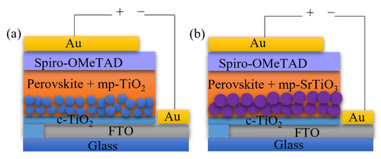
Figure 1.
Architecture of (a) mp-TiO2- and (b) mp-SrTiO3-based PSC devices.
A c-TiO2 layer may effectively work as a hole blocking layer, which helps to reduce recombination losses and thus to improve photovoltaic performance, and thus commonly used in high performance PSCs [3,4,56,57]. Figure 2 shows that a uniform and pinhole-free c-TiO2 layer with a thickness of 50 nm can be successfully deposited by inkjet printing, and that the compact TiO2 layer crystallized with an anatase crystal structure.
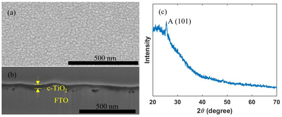
Figure 2.
(a) Top view; (b) cross section SEM images; and (c) XRD pattern of an inkjet-printed c-TiO2 layer.
A major challenge for inkjet printing of high-quality thin films is to eliminate the ‘coffee-ring’ effect, which often occurs when the solvent of a drop containing dispersed solids evaporates and the nonvolatile solid components assemble at the periphery of the drop due to the outward capillary flow and pinned contact line [58,59]. To suppress the coffee-ring effect and control the film morphology, intense efforts were made in the literature and different approaches were proposed, such as solvent composition engineering [60,61], contact line depinning [59,62], evaporation temperature adjustment [63,64], and particle modification [65]. For inkjet printing, the optimization of the ink properties is the most common strategy to improve the film uniformity. Therefore, the selection of solvents for the solutions, and especially for nanoparticle dispersions, is crucial. The emphasis was focused on the physicochemical properties of the solvents, such as the viscosity and surface tension [66,67], which control the ink printability, film formation, and clogging mitigation of the nozzles within the printhead. A cosolvent system is widely used to control the morphology because of the inward Marangoni flow induced by the surface-tension gradients [53,54]. In the present work, we optimized the solvent composition for nanoparticle suspensions aimed at high device performance. The viscosity and surface tension of the inks were in the range of 1–25 mPa·s and 20–50 mN·m−1. Table 1 and Figure 3 demonstrate the effect of the solvent 2-isopropoxyethanol (IPE) and the mixed solvent ethanol: ethylene glycol (EtOH:EG = 9:1, v:v), used for dispersing TiO2 nanoparticles, on the photovoltaic performance of TiO2-based devices. For each set of solvents, 12 devices were manufactured. The average and champion photovoltaic parameters, including VOC, JSC, fill factor (FF) and PCE, are listed in Table 1 and the statistical distribution is illustrated in Figure 3. The series resistance (Rs) and shunt resistance (Rsh) are also estimated from the inverse of the slope of the J-V curves at the region of the Voc and the Jsc, respectively. Although Device S1 displayed a higher champion PCE than Device S2 (Figure S2), Device S2 offered a slightly higher average PCE of 10.97%, as compared to 10.64% of Device S1. From Figure 4a,b, the difference in the drying mechanics of the solvent IPE and EtOH:EG leads to also a difference in the microstructure (Figure S3) of the resulting mp-TiO2 film. A thicker ETL could allow more perovskite to be absorbed to absorb more incident light but may also lead to a larger series resistance causing Device S1 to exhibit a higher JSC and a lower FF than Device S2. With a higher TiO2 nanoparticle ink concentration, Device S3 showed an increase in JSC and a decrease in FF due to the formation of a thicker mesoporous TiO2 layer, as compared to Device S2. Eventually, as seen in Figure 3, although there is no considerable difference in PCE between Device S1, S2, and S3, Device S3 showed the best reproducibility ascribed to the microstructure of mp-TiO2(Figure 4c) inkjet-printed with TiO2 inks based on the mixed solvent EtOH:EG.

Table 1.
Photovoltaic parameters from the current density-voltage (J-V) characteristics of mp-TiO2- and mp-SrTiO3-based PSCs. Each average value is based on 12 devices.
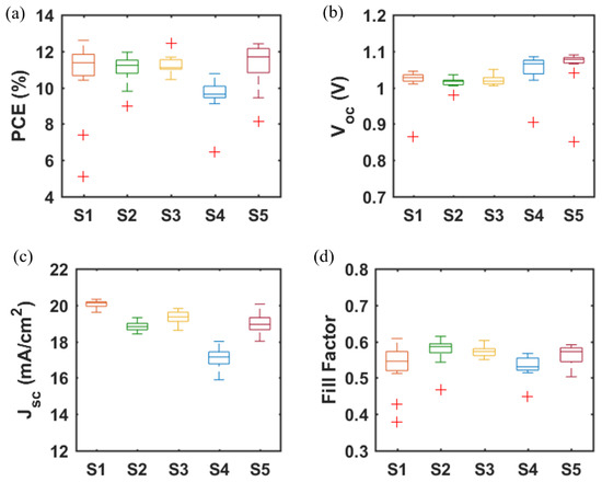
Figure 3.
(a) PCE, (b) VOC, (c) JSC, and (d) FF of PSCs based on mp-TiO2 and mp-SrTiO3 ETLs inkjet-printed from nanoparticle inks with IPE or EtOH:EG as solvents. Data are obtained from 12 devices for each type of PSC. (Boxplots, red + signs represent outliers).
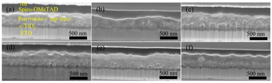
Figure 4.
Cross-section SEM images of Device (a) S1, (b) S2, (c) S3, (d) S4, (e) S5, and (f) a spin-coated, TiO2-based PSC.
Furthermore, we fabricated SrTiO3-based Device S4 and Device S5 by inkjet printing of SrTiO3 nanoparticle inks with IPE and EtOH:EG as solvents, respectively. From Figure 3, it can be noted that Device S5 exhibits a higher efficiency with substantial improvements in all photovoltaic parameters, as compared to that of Device S4. A capping layer of perovskite on top of the ETL is beneficial for the improved performance because direct contact between ETL and the hole transport layer thereby is avoided, and thus recombination losses reduced. As seen in Figure 4d,e, the more porous structure of the mp-SrTiO3 films in Device S4 (Figure S3) results in a thinner capping perovskite layer, thereby causing more pronounced recombination losses and consequently accounting for the lower device performance.
Figure 3 also demonstrates that the photovoltaic performance of the SrTiO3-based Device S5 is comparable to that of TiO2-based devices. The VOC of SrTiO3-based solar cells is higher than that of the TiO2-based counterparts. A reason for the higher photovoltages is that a higher conduction band edge energy level and a smaller band edge offset of the SrTiO3 (Figure 5) will result in a higher VOC [17,18]. Another reason is that a capping perovskite layer is clearly observed in SrTiO3-based devices (Figure 4d,e) but not in TiO2-based devices (Figure 4b,c), thereby reducing the direct shunt loss path and yielding a higher VOC. The lower JSC obtained from SrTiO3-based devices as compared to that of TiO2-based devices is because of the limited loading of perovskite, caused by the smaller effective surface area of mp-SrTiO3 owing to the larger SrTiO3 nanoparticles [17,68].
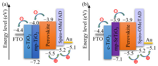
Figure 5.
Schematics of the energy levels of (a) mp-TiO2- and (b) mp-SrTiO3-based PSCs.
The photovoltaic performance of mp-SrTiO3-based PSCs was further optimized. As seen in Table 2 and Figure 6, with lower concentrations of SrTiO3 in the nanoparticle inks, the performance of mp-SrTiO3-based PSCs is improved with higher VOC, JSC and FF. The main reason can be attributed to the ink concentrations which influence the thickness and microstructure of the inkjet-printed mp-SrTiO3 layer (Figure 7). Furthermore, inkjet-printed SrTiO3-based devices based on a 0.15 M SrTiO3 ink showed a PCE of 14.56%. Higher VOC is obtained for PSCs manufactured from 0.15 M SrTiO3 inks as compared to that of TiO2-based devices, as mentioned before. However, the recorded JSC is much lower since SrTiO3 nanoparticles with a large size express a smaller effective surface area, which limits the overall interfacial area between the perovskite layer and the ETL [20]. Therefore, this can result in an inefficient charge transfer in SrTiO3-based devices accounting for the pronounced scan-direction hysteresis observed, as shown in Figure 8, and the large difference in the overall performance for the two opposite scan directions. This dependence on the scan direction is much more pronounced in devices made from 0.15 M SrTiO3 inks than in TiO2-based ones. Another reason could be that SrTiO3-based cells demonstrate a larger Rs than TiO2-based ones. A higher Rs causes larger charge loss at high bias voltages and results in an inefficient charge transfer in the forward scan direction. In addition, the resulting SrTiO3 ETL (Figure 7c) printed from 0.15 M SrTiO3 inks is quite thin at some positions, which may cause the direct contact between the compact layer and the perovskite layer and then lead to recombination losses, thereby resulting in the pronounced hysteresis in SrTiO3-based PSCs.
Table 2.
Photovoltaic parameters from J-V characteristics of mp-SrTiO3-based PSCs inkjet-printed with inks of different concentrations. Each average value is based on 9 devices.
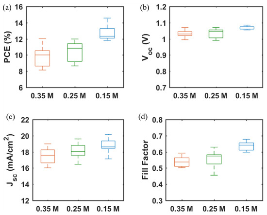
Figure 6.
(a) PCE, (b) VOC, (c) JSC, and (d) FF of PSCs based on mp-SrTiO3 ETLs inkjet-printed with SrTiO3 nanoparticle inks of different concentrations. Data are obtained from 9 devices of each type.
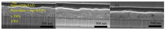
Figure 7.
Cross-section SEM images of SrTiO3-based PSCs inkjet-printed using (a) 0.35 M, (b) 0.25 M, and (c) 0.15 M inks.
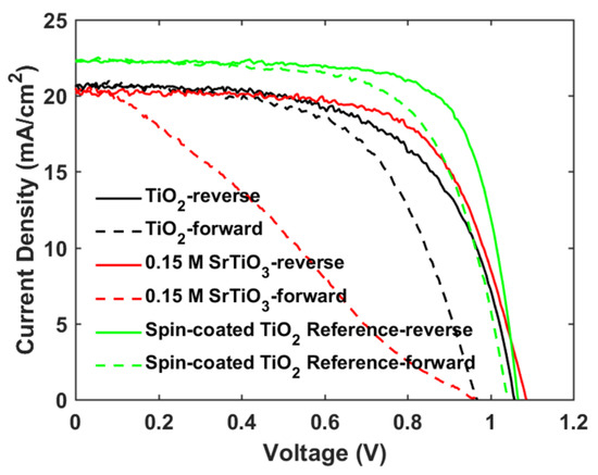
Figure 8.
Reverse and forward scan J-V curves of mp-TiO2- and mp-SrTiO3-based PSCs.
To increase the JSC and suppress the hysteresis observed in SrTiO3-based PSCs, a small amount of TiO2 nanoparticles was added to the SrTiO3 nanoparticle inks to generate a mixed mesoporous SrTiO3/TiO2 ETL [21]. From Table 3 and Figure 9, the photovoltaic performance of SrTiO3/TiO2-based PSCs is improved as compared to SrTiO3-based PSCs, and the devices display a highest PCE of 15.73% with VOC = 1.11V, JSC = 20.99 mA/cm2 and FF = 0.68 (TiO2 concentration is 10 wt.% with respect to SrTiO3). The VOC shows a negligible change, while both JSC and FF increase and then decrease with TiO2 concentration ranging from 0 to 20%. Firstly, with introducing the smaller TiO2 nanoparticles to the SrTiO3 ETL, the interfacial area between the perovskite layer and the ETL will increase, and thus the JSC is expected to increase. The smaller TiO2 nanoparticles could also fill the pores between the larger SrTiO3 nanoparticles and as well at the surface of the mesoporous ETL, which is beneficial for increasing the FF. With the TiO2 concentration further increased from 10% to 20%, the electrical resistance of the SrTiO3/TiO2 ETL will increase, resulting in a decrease in JSC and FF.
Table 3.
Average photovoltaic parameters for mp-SrTiO3/TiO2-based PSCs inkjet-printed with inks of different TiO2 concentrations. Each average value is based on 5 devices.
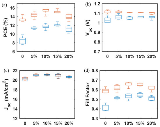
Figure 9.
TiO2 concentration-dependent photovoltaic parameters (a) PCE, (b) VOC, (c) JSC, and (d) FF for mp-SrTiO3/TiO2-based PSCs. Red boxes and blue boxes represent data from reverse and forward scan directions, respectively.
The main objective of the formulating nanoparticle mixtures, the severe hysteresis problem, is indeed found to become suppressed for the mixed SrTiO3/TiO2-based PSCs, as shown in Table 4 and Figure 10. A hysteresis index is normally used to describe the performance difference between the reverse and forward scan direction and is defined by
where and represent the power conversion efficiency from the reverse and forward scan directions, respectively. The hysteresis index decreases by 34% when the TiO2 concentration is increased from 0% to 10%, and the charge-transfer ability of the mp-SrTiO3/TiO2 ETL apparently is improved.
Table 4.
Average hysteresis index for mp-SrTiO3/TiO2-based PSCs inkjet-printed with inks of different TiO2 concentrations.
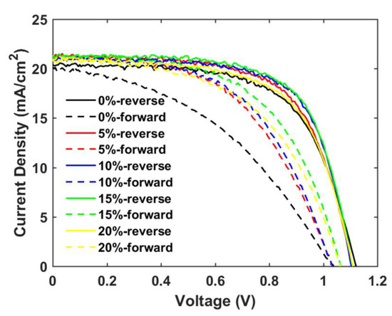
Figure 10.
Reverse and forward scan J-V curves of champion cells of mp-SrTiO3/TiO2-based PSCs inkjet-printed with inks of different TiO2 concentrations.
Furthermore, we fabricated PSCs based on an inkjet-printed SnO2 ETL layer with a configuration as illustrated in Figure 11. Also in this system, we used a cosolvent system for printing the SnO2 thin films from the commercial SnO2 colloidal dispersion. Water works as the main solvent, and ethylene glycol and Triton are used to control the drying properties and to adjust the viscosity and surface tension for high-quality printing results. The details for preparing the SnO2 ink are described in the experimental section. The top SEM image of the inkjet-printed SnO2 thin film is shown in Figure S4. By optimizing the SnO2 thickness through changes of the ink concentration, we obtained a best performing cell with a PCE of 17.37% with a VOC of 1.10V, JSC of 21.13 mA/cm2, and FF of 0.75, and the J-V characteristics are shown in Figure 12a. We also recorded the steady-state current density of the champion cell at the maximum power point Vmpp = 0.925 V. As seen in Figure 12b, a steady-state current density of 21.05 mA/cm2 and a stabilized PCE of 17.30% were obtained, which agree well with the JSC and PCE extracted from the J-V experiments. The average photovoltaic parameters of PSCs based on SnO2 ETLs printed with inks of different concentrations are shown in Table 5. When the SnO2 ink concentration is increased from 0.375% to 3%, the PCE (Figure S5) of SnO2-based PSCs decreases continuously. As seen in the cross-sectional SEM images in Figure 13, the SnO2 thickness increases from 30 nm to 130 nm when the ink concentration is increased from 0.375% to 3%. Too thick SnO2 films result in large sheet resistances, hampering charge transfer, thereby leading to lower PCEs.
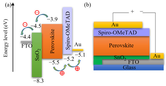
Figure 11.
Schematics of (a) energy levels and (b) configuration of SnO2-based PSCs.
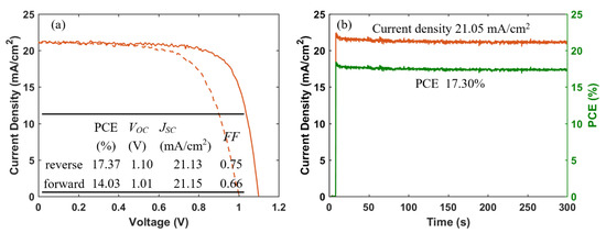
Figure 12.
(a) J-V curves (solid and dashed lines represent data from reverse and forward scan, respectively), and (b) steady-state current density (at a bias of 0.925 V) and PCE of champion cell of PSCs based on inkjet-printed SnO2 ETLs.
Table 5.
Photovoltaic parameters for PSCs based on inkjet-printed SnO2 ETLs prepared from different ink concentrations. Averages are based on different number of cells, as indicated in second column.
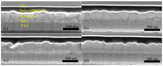
Figure 13.
Cross-sectional SEM images for PSCs based on inkjet-printed SnO2 ETLs prepared from (a) 0.375%, (b) 0.75%, (c) 1.5%, and (d) 3% precursor inks.
As compared to that of TiO2- and SrTiO3-based PSCs, the SnO2-based congeners show less hysteresis, as well as better performance because of the superior electrical properties of the SnO2 material, such as high electron mobility [26]. Therefore, highly efficient perovskite solar cells based on inkjet-printed SnO2 ETLs should be attainable after a thorough optimization.
4. Conclusions
In this work, we developed the inkjet printing processes for TiO2, SrTiO3, and SnO2 ETLs. By optimizing the PSC performance based on the printed ETLs, the drying properties of cosolvent inks are beneficial for uniform film formation of the mesoporous TiO2 and SrTiO3 ETLs. Although SrTiO3-based PSCs perform better than TiO2-based ones, the former devices suffer from low current density and severe scan-direction hysteresis. PSCs based on the mixed mesoporous SrTiO3/TiO2 ETL can mitigate these problems and offer a higher PCE than the SrTiO3-only based devices. Furthermore, the strategy using cosolvent inks was also applied for inkjet printing of SnO2 ETLs. The best performing SnO2-based PSCs displayed an optimal PCE of 17.37% and low scan-direction hysteresis. In summary, the printing processes for different ETL materials were developed and will be used for fully inkjet-printed PSCs in our future work.
Supplementary Materials
The following are available online at https://www.mdpi.com/article/10.3390/ma14247525/s1, Figure S1: Device geometry of perovskite solar cells, Figure S2: J-V curves of champion PSCs based on mp-TiO2 and mp-SrTiO3 ETLs inkjet-printed from nanoparticle inks with IPE or EtOH:EG as solvents, Figure S3: SEM images of mesoporous layers inkjet-printed from (a) TiO2 inks with the solvent IPE, (b) TiO2 inks with the solvent EtOH:EG, (c) SrTiO3 inks with the solvent IPE, and (d) SrTiO3 inks with the solvent EtOH:EG, Figure S4: SEM image of inkjet-printed SnO2 thin film, Figure S5: J-V curves of champion PSCs based on inkjet-printed SnO2 ETLs prepared from 0.375%, 0.75%, 1.5%, and 3% precursor inks, Table S1: Technical information of the printhead XJ126/50 and XJ126/80. These parameters are obtained from the Xaar126 data sheet.
Author Contributions
Conceptualization, D.L. and L.B.; methodology, D.L. and W.Z.; validation, D.L. and W.Z.; formal analysis, D.L.; investigation, D.L., W.Z. and L.B.; resources, L.K. and L.B.; data curation, D.L.; writing—original draft preparation, D.L.; writing—review and editing, D.L., W.Z., L.K. and L.B.; visualization, D.L.; supervision, L.B. and L.K.; project administration, L.B.; funding acquisition, D.L. and L.B. All authors have read and agreed to the published version of the manuscript.
Funding
This research was funded by the China Scholarship Council (CSC), the Swedish Research Council (VR), grant number 2017-04875, and the Carl Trygger Foundation.
Institutional Review Board Statement
Not applicable.
Informed Consent Statement
Not applicable.
Data Availability Statement
The data presented in this study are available on request from the corresponding author.
Acknowledgments
Authors acknowledge Resource Center for Coordination of Electron Microscopy at KTH and Anastasia Riazanova (Dept. of Fibre and Polymer Technology) for the help with part of SEM analysis.
Conflicts of Interest
The authors declare no conflict of interest. The funders had no role in the design of the study; in the collection, analyses, or interpretation of data; in the writing of the manuscript, or in the decision to publish the results.
References
- Tavakoli, M.M.; Giordano, F.; Zakeeruddin, S.M.; Grätzel, M. Mesoscopic Oxide Double Layer as Electron Specific Contact for Highly Efficient and UV Stable Perovskite Photovoltaics. Nano Lett. 2018, 18, 2428–2434. [Google Scholar] [CrossRef]
- Lee, Y.; Paek, S.; Cho, K.T.; Oveisi, E.; Gao, P.; Lee, S.; Park, J.-S.; Zhang, Y.; Humphry-Baker, R.; Asiri, A.M.; et al. Enhanced charge collection with passivation of the tin oxide layer in planar perovskite solar cells. J. Mater. Chem. A 2017, 5, 12729–12734. [Google Scholar] [CrossRef]
- Jeon, N.J.; Noh, J.H.; Kim, Y.C.; Yang, W.S.; Ryu, S.; Seok, S.I. Solvent engineering for high-performance inorganic–organic hybrid perovskite solar cells. Nat. Mater. 2014, 13, 897–903. [Google Scholar] [CrossRef] [PubMed]
- Jeong, I.; Park, Y.H.; Bae, S.; Park, M.; Jeong, H.; Lee, P.; Ko, M.J. Solution-Processed Ultrathin TiO2 Compact Layer Hybridized with Mesoporous TiO2 for High-Performance Perovskite Solar Cells. ACS Appl. Mater. Interfaces 2017, 9, 36865–36874. [Google Scholar] [CrossRef]
- Jung, E.H.; Jeon, N.J.; Park, E.Y.; Moon, C.S.; Shin, T.J.; Yang, T.-Y.; Noh, J.H.; Seo, J. Efficient, stable and scalable perovskite solar cells using poly(3-hexylthiophene). Nat. Cell Biol. 2019, 567, 511–515. [Google Scholar] [CrossRef]
- Kim, M.; Kim, G.-H.; Lee, T.K.; Choi, I.W.; Choi, H.W.; Jo, Y.; Yoon, Y.J.; Kim, J.W.; Lee, J.; Huh, D.; et al. Methylammonium Chloride Induces Intermediate Phase Stabilization for Efficient Perovskite Solar Cells. Joule 2019, 3, 2179–2192. [Google Scholar] [CrossRef]
- NREL. Best Research-Cell Efficiency Chart. Available online: https://www.nrel.gov/pv/cell-efficiency.html (accessed on 12 January 2021).
- Tsvetkov, N.; Moon, B.C.; Lee, J.Y.; Kang, J.K. Controlled Synthesis of Nanocrystalline Nb:SrTiO3 Electron Transport Layers for Robust Interfaces and Stable High Photovoltaic Energy Conversion Efficiency in Perovskite Halide Solar Cells. ACS Appl. Energy Mater. 2020, 3, 344–351. [Google Scholar] [CrossRef]
- Yi, H.; Wang, D.; Mahmud, M.A.; Haque, F.; Upama, M.B.; Xu, C.; Duan, L.; Uddin, A. Bilayer SnO2 as Electron Transport Layer for Highly Efficient Perovskite Solar Cells. ACS Appl. Energy Mater. 2018, 1, 6027–6039. [Google Scholar] [CrossRef]
- Giordano, F.; Abate, A.; Baena, J.-P.C.; Saliba, M.; Matsui, T.; Im, S.H.; Zakeeruddin, S.M.; Nazeeruddin, M.K.; Hagfeldt, A.; Graetzel, M. Enhanced electronic properties in mesoporous TiO2 via lithium doping for high-efficiency perovskite solar cells. Nat. Commun. 2016, 7, 10379. [Google Scholar] [CrossRef] [PubMed]
- Chen, L.; Zhou, Y.; Tu, W.; Li, Z.; Bao, C.; Dai, H.; Yu, T.; Liu, J.; Zou, Z. Enhanced photovoltaic performance of a dye-sensitized solar cell using graphene–TiO2 photoanode prepared by a novel in situ simultaneous reduction-hydrolysis technique. Nanoscale 2013, 5, 3481–3485. [Google Scholar] [CrossRef]
- Wang, J.T.-W.; Ball, J.M.; Barea, E.M.; Abate, A.; Alexander-Webber, J.A.; Huang, J.; Saliba, M.; Mora-Sero, I.; Bisquert, J.; Snaith, H.J.; et al. Low-Temperature Processed Electron Collection Layers of Graphene/TiO2 Nanocomposites in Thin Film Perovskite Solar Cells. Nano Lett. 2014, 14, 724–730. [Google Scholar] [CrossRef] [PubMed]
- Wojciechowski, K.; Stranks, S.D.; Abate, A.; Sadoughi, G.; Sadhanala, A.; Kopidakis, N.; Rumbles, G.; Li, C.-Z.; Friend, R.H.; Jen, A.K.-Y.; et al. Heterojunction Modification for Highly Efficient Organic–Inorganic Perovskite Solar Cells. ACS Nano 2014, 8, 12701–12709. [Google Scholar] [CrossRef] [PubMed]
- Li, T.; Rui, Y.; Zhang, X.; Shi, J.; Wang, X.; Wang, Y.; Yang, J.; Zhang, Q. Anatase TiO2 nanorod arrays as high-performance elec-tron transport layers for perovskite solar cells. J. Alloys Compd. 2020, 849, 156629. [Google Scholar] [CrossRef]
- Choi, J.; Song, S.; Hörantner, M.T.; Snaith, H.J.; Park, T. Well-Defined Nanostructured, Single-Crystalline TiO2 Electron Transport Layer for Efficient Planar Perovskite Solar Cells. ACS Nano 2016, 10, 6029–6036. [Google Scholar] [CrossRef] [PubMed]
- Hou, Y.; Chen, X.; Yang, S.; Li, C.; Zhao, H.; Yang, H.G. A Band-Edge Potential Gradient Heterostructure to Enhance Electron Extraction Efficiency of the Electron Transport Layer in High-Performance Perovskite Solar Cells. Adv. Funct. Mater. 2017, 27, 1700878. [Google Scholar] [CrossRef]
- Bera, A.; Wu, K.W.; Sheikh, A.; Alarousu, E.; Mohammed, O.F.; Wu, T. Perovskite Oxide SrTiO3 as an Efficient Electron Transporter for Hybrid Perovskite Solar Cells. J. Phys. Chem. C 2014, 118, 28494–28501. [Google Scholar] [CrossRef]
- Neophytou, M.; de Bastiani, M.; Gasparini, N.; Aydin, E.; Ugur, E.; Seitkhan, A.; Moruzzi, F.; Choaie, Y.; Ramadan, A.J.; Troughton, J.R.; et al. Enhancing the Charge Extraction and Stability of Perovskite Solar Cells Using Strontium Titanate (SrTiO3) Electron Transport Layer. ACS Appl. Energy Mater. 2019, 2, 8090–8097. [Google Scholar] [CrossRef]
- Wang, C.; Tang, Y.; Hu, Y.; Huang, L.; Fu, J.; Jin, J.; Shi, W.; Wang, L.; Yang, W. Graphene/SrTiO3nanocomposites used as an effective electron-transporting layer for high-performance perovskite solar cells. RSC Adv. 2015, 5, 52041–52047. [Google Scholar] [CrossRef]
- Hu, Y.; Wang, C.; Tang, Y.; Huang, L.; Fu, J.; Shi, W.; Wang, L.; Yang, W. Three-dimensional self-branching anatase TiO2 nanorods with the improved carrier collection for SrTiO3-based perovskite solar cells. J. Alloys Compd. 2016, 679, 32–38. [Google Scholar] [CrossRef]
- Okamoto, Y.; Fukui, R.; Fukazawa, M.; Suzuki, Y. SrTiO3/TiO2 composite electron transport layer for perovskite solar cells. Mater. Lett. 2017, 187, 111–113. [Google Scholar] [CrossRef][Green Version]
- Mahmoudi, T.; Wang, Y.; Hahn, Y.-B. SrTiO3/Al2O3-Graphene Electron Transport Layer for Highly Stable and Efficient Com-posites-Based Perovskite Solar Cells with 20.6% Efficiency. Adv. Energy Mater. 2020, 10, 1903369. [Google Scholar] [CrossRef]
- Yeom, E.J.; Shin, S.S.; Yang, W.S.; Lee, S.J.; Yin, W.; Kim, D.; Noh, J.H.; Ahn, T.K.; Seok, S.I. Controllable synthesis of single crystalline Sn-based oxides and their application in perovskite solar cells. J. Mater. Chem. A 2017, 5, 79–86. [Google Scholar] [CrossRef]
- Jiang, Q.; Zhao, Y.; Zhang, X.; Yang, X.; Chen, Y.; Chu, Z.; Ye, Q.; Li, X.; Yin, Z.; You, J. Surface passivation of perovskite film for efficient solar cells. Nat. Photonics 2019, 13, 460–466. [Google Scholar] [CrossRef]
- Ke, W.; Fang, G.; Liu, Q.; Xiong, L.; Qin, P.; Tao, H.; Wang, J.; Lei, H.; Li, B.; Wan, J.; et al. Low-Temperature Solution-Processed Tin Oxide as an Alternative Electron Transporting Layer for Efficient Perovskite Solar Cells. J. Am. Chem. Soc. 2015, 137, 6730–6733. [Google Scholar] [CrossRef] [PubMed]
- Jiang, Q.; Zhang, L.; Wang, H.; Yang, X.; Meng, J.; Liu, H.; Yin, Z.; Wu, J.; Zhang, X.; You, J. Enhanced electron extraction using SnO2 for high-efficiency planar-structure HC(NH2)2PbI3-based perovskite solar cells. Nat. Energy 2017, 2, 16177. [Google Scholar] [CrossRef]
- Anaraki, E.H.; Kermanpur, A.; Steier, L.; Domanski, K.; Matsui, T.; Tress, W.; Saliba, M.; Abate, A.; Grätzel, M.; Hagfeldt, A.; et al. Highly efficient and stable planar perovskite solar cells by solution-processed tin oxide. Energy Environ. Sci. 2016, 9, 3128–3134. [Google Scholar] [CrossRef]
- Zhu, Z.; Bai, Y.; Liu, X.; Chueh, C.-C.; Yang, S.; Jen, A.K.-Y. Enhanced Efficiency and Stability of Inverted Perovskite Solar Cells Using Highly Crystalline SnO2 Nanocrystals as the Robust Electron-Transporting Layer. Adv. Mater. 2016, 28, 6478–6484. [Google Scholar] [CrossRef] [PubMed]
- Xiong, L.; Qin, M.; Chen, C.; Wen, J.; Yang, G.; Guo, Y.; Ma, J.; Zhang, Q.; Qin, P.; Li, S.; et al. Fully High-Temperature-Processed SnO2as Blocking Layer and Scaffold for Efficient, Stable, and Hysteresis-Free Mesoporous Perovskite Solar Cells. Adv. Funct. Mater. 2018, 28, 1706276. [Google Scholar] [CrossRef]
- Li, Y.; Zhu, J.; Huang, Y.; Liu, F.; Lv, M.; Chen, S.; Hu, L.; Tang, J.; Yao, J.; Dai, S. Mesoporous SnO2 nanoparticle films as elec-tron-transporting material in perovskite solar cells. RSC Adv. 2015, 5, 28424–28429. [Google Scholar] [CrossRef]
- Ren, X.; Yang, D.; Yang, Z.; Feng, J.; Zhu, X.; Niu, J.; Liu, Y.; Zhao, W.; Liu, S.F. Solution-Processed Nb:SnO2 Electron Transport Layer for Efficient Planar Perovskite Solar Cells. ACS Appl. Mater. Interfaces 2017, 9, 2421–2429. [Google Scholar] [CrossRef]
- Yang, G.; Lei, H.; Tao, H.; Zheng, X.; Ma, J.; Liu, Q.; Ke, W.; Chen, Z.; Xiong, L.; Qin, P.; et al. Reducing Hysteresis and Enhancing Performance of Perovskite Solar Cells Using Low-Temperature Processed Y-Doped SnO2Nanosheets as Electron Selective Layers. Small 2017, 13, 1601769. [Google Scholar] [CrossRef] [PubMed]
- Roose, B.; Johansen, C.M.; Dupraz, K.; Jaouen, T.; Aebi, P.; Steiner, U.; Abate, A. A Ga-doped SnO2 mesoporous contact for UV stable highly efficient perovskite solar cells. J. Mater. Chem. A 2018, 6, 1850–1857. [Google Scholar] [CrossRef]
- Jung, E.H.; Chen, B.; Bertens, K.; Vafaie, M.; Teale, S.; Proppe, A.H.; Hou, Y.; Zhu, T.; Zheng, C.; Sargent, E.H. Bifunctional Surface Engineering on SnO2 Reduces Energy Loss in Perovskite Solar Cells. ACS Energy Lett. 2020, 5, 2796–2801. [Google Scholar] [CrossRef]
- Zhang, M.; Wu, F.; Chi, D.; Shi, K.; Huang, S. High-efficiency perovskite solar cells with poly(vinylpyrrolidone)-doped SnO2 as an electron transport layer. Mater. Adv. 2020, 1, 617–624. [Google Scholar] [CrossRef]
- Huang, X.; Hu, Z.; Xu, J.; Wang, P.; Wang, L.; Zhang, J.; Zhu, Y. Low-temperature processed SnO2 compact layer by incorporating TiO2 layer toward efficient planar heterojunction perovskite solar cells. Sol. Energy Mater. Sol. Cells 2017, 164, 87–92. [Google Scholar] [CrossRef]
- Zhao, X.; Tao, L.; Li, H.; Huang, W.; Sun, P.; Liu, J.; Liu, S.; Sun, Q.; Cui, Z.; Sun, L.; et al. Efficient Planar Perovskite Solar Cells with Improved Fill Factor via Interface Engineering with Graphene. Nano Lett. 2018, 18, 2442–2449. [Google Scholar] [CrossRef]
- Huckaba, A.J.; Lee, Y.; Xia, R.; Paek, S.; Bassetto, V.C.; Oveisi, E.; Lesch, A.; Kinge, S.; Dyson, P.J.; Girault, H.; et al. Inkjet-Printed Mesoporous TiO2 and Perovskite Layers for High Efficiency Perovskite Solar Cells. Energy Technol. 2019, 7, 317–324. [Google Scholar] [CrossRef]
- Buffiere, M.; Ali, K.; Fares, E.; Samara, A.; Shetty, A.R.; Al Hassan, O.; Belaidi, A. Inkjet-Printed Compact TiO 2 Electron Transport Layer for Perovskite Solar Cells. Energy Technol. 2020, 8, 2000330. [Google Scholar] [CrossRef]
- Rohnacher, V.; Ullrich, F.; Eggers, H.; Schackmar, F.; Hell, S.; Salazar, A.; Huck, C.; Hernandez-Sosa, G.; Paetzold, U.W.; Jaegermann, W.; et al. Analytical Study of Solution-Processed Tin Oxide as Electron Transport Layer in Printed Perovskite Solar Cells. Adv. Mater. Technol. 2021, 6, 2000282. [Google Scholar] [CrossRef]
- Xie, M.; Lu, H.; Zhang, L.; Wang, J.; Luo, Q.; Lin, J.; Ba, L.; Liu, H.; Shen, W.; Shi, L.; et al. Fully Solution-Processed Semi-Transparent Perovskite Solar Cells with Ink-Jet Printed Silver Nanowires Top Electrode. Sol. RRL 2018, 2, 1700184. [Google Scholar] [CrossRef]
- Li, S.-G.; Jiang, K.-J.; Su, M.-J.; Cui, X.-P.; Huang, J.-H.; Zhang, Q.-Q.; Zhou, X.-Q.; Yang, L.-M.; Song, Y.-L. Inkjet printing of CH3NH3PbI3 on a mesoscopic TiO2 film for highly efficient perovskite solar cells. J. Mater. Chem. A 2015, 3, 9092–9097. [Google Scholar] [CrossRef]
- Gheno, A.; Huang, Y.; Bouclé, J.; Ratier, B.; Rolland, A.; Even, J.; Vedraine, S. Toward Highly Efficient Inkjet-Printed Perovskite Solar Cells Fully Processed Under Ambient Conditions and at Low Temperature. Sol. RRL 2018, 2, 1800191. [Google Scholar] [CrossRef]
- Mathies, F.; Eggers, H.; Richards, B.S.; Hernandez-Sosa, G.; Lemmer, U.; Paetzold, U.W. Inkjet-Printed Triple Cation Perovskite Solar Cells. ACS Appl. Energy Mater. 2018, 1, 1834–1839. [Google Scholar] [CrossRef]
- Eggers, H.; Schackmar, F.; Abzieher, T.; Sun, Q.; Lemmer, U.; Vaynzof, Y.; Richards, B.; Hernandez-Sosa, G.; Paetzold, U.W. Inkjet-Printed Micrometer-Thick Perovskite Solar Cells with Large Columnar Grains. Adv. Energy Mater. 2020, 10, 1903184. [Google Scholar] [CrossRef]
- Schackmar, F.; Eggers, H.; Frericks, M.; Richards, B.S.; Lemmer, U.; Hernandez-Sosa, G.; Paetzold, U.W. Perovskite Solar Cells with All-Inkjet-Printed Absorber and Charge Transport Layers. Adv. Mater. Technol. 2021, 6, 2000271. [Google Scholar] [CrossRef]
- Jung, K.-H.; Seo, J.-Y.; Lee, S.; Shin, H.; Park, N.-G. Solution-processed SnO2thin film for a hysteresis-free planar perovskite solar cell with a power conversion efficiency of 19.2%. J. Mater. Chem. A 2017, 5, 24790–24803. [Google Scholar] [CrossRef]
- Wang, C.; Zhao, D.; Grice, C.R.; Liao, W.; Yu, Y.; Cimaroli, A.; Shrestha, N.; Roland, P.J.; Chen, J.; Yu, Z.; et al. Low-temperature plasma-enhanced atomic layer deposition of tin oxide electron selective layers for highly efficient planar perovskite solar cells. J. Mater. Chem. A 2016, 4, 12080–12087. [Google Scholar] [CrossRef]
- Ma, J.; Zheng, X.; Lei, H.; Ke, W.; Chen, C.; Chen, Z.; Yang, G.; Fang, G. Highly Efficient and Stable Planar Perovskite Solar Cells with Large-Scale Manufacture of E-Beam Evaporated SnO2 Toward Commercialization. Sol. RRL 2017, 1, 1700118. [Google Scholar] [CrossRef]
- Liu, X.; Tsai, K.-W.; Zhu, Z.; Sun, Y.; Chueh, C.-C.; Jen, A.K.-Y. A Low-Temperature, Solution Processable Tin Oxide Electron-Transporting Layer Prepared by the Dual-Fuel Combustion Method for Efficient Perovskite Solar Cells. Adv. Mater. Interfaces 2016, 3, 1600122. [Google Scholar] [CrossRef]
- Zhang, W.; Liu, P.; Sadollahkhani, A.; Li, Y.; Zhang, B.; Zhang, F.; Safdari, M.; Hao, Y.; Hua, Y.; Kloo, L. Investigation of Tri-phenylamine (TPA)-Based Metal Complexes and Their Application in Perovskite Solar Cells. ACS Omega 2017, 2, 9231–9240. [Google Scholar] [CrossRef]
- Bernacka-Wojcik, I.; Wojcik, P.J.; Aguas, H.; Fortunato, E.; Martins, R. Inkjet printed highly porous TiO 2 films for improved electrical properties of photoanode. J. Colloid Interface Sci. 2016, 465, 208–214. [Google Scholar] [CrossRef]
- Cherrington, R.; Hughes, D.J.; Senthilarasu, S.; Goodship, V. Inkjet-Printed TiO2Nanoparticles from Aqueous Solutions for Dye-Sensitized Solar Cells (DSSCs). Energy Technol. 2015, 3, 866–870. [Google Scholar] [CrossRef]
- Oh, Y.; Yoon, H.G.; Lee, S.-N.; Kim, H.-K.; Kim, J. Inkjet-Printing of TiO2Co-Solvent Ink: From Uniform Ink-Droplet to TiO2 Photoelectrode for Dye-Sensitized Solar Cells. J. Electrochem. Soc. 2011, 159, B34–B38. [Google Scholar] [CrossRef]
- Kunugi, Y.; Shimoyama, Y.; Umezu, S. Fabrication of Dye-sensitized Solar Cells Using Electrostatic Inkjet Printing. J. Photopolym. Sci. Technol. 2013, 26, 383–385. [Google Scholar] [CrossRef][Green Version]
- Peng, B.; Jungmann, G.; Jäger, C.; Haarer, D.; Schmidt, H.-W.; Thelakkat, M. Systematic investigation of the role of compact TiO2 layer in solid state dye-sensitized TiO2 solar cells. Co-Ord. Chem. Rev. 2004, 248, 1479–1489. [Google Scholar] [CrossRef]
- Wu, Y.; Yang, X.; Chen, H.; Zhang, K.; Qin, C.; Liu, J.; Peng, W.; Islam, A.; Bi, E.; Ye, F.; et al. Highly compact TiO2 layer for efficient hole-blocking in perovskite solar cells. Appl. Phys. Express 2014, 7, 052301. [Google Scholar] [CrossRef]
- Deegan, R.D.; Bakajin, O.; Dupont, T.F.; Huber, G.; Nagel, S.R.; Witten, T.A. Capillary flow as the cause of ring stains from dried liquid drops. Nature 1997, 389, 827. [Google Scholar] [CrossRef]
- Li, Y.-F.; Sheng, Y.-J.; Tsao, H.-K. Evaporation Stains: Suppressing the Coffee-Ring Effect by Contact Angle Hysteresis. Langmuir 2013, 29, 7802–7811. [Google Scholar] [CrossRef] [PubMed]
- Kim, D.; Jeong, S.; Park, B.K.; Moon, J. Direct writing of silver conductive patterns: Improvement of film morphology and conductance by controlling solvent compositions. Appl. Phys. Lett. 2006, 89, 264101. [Google Scholar] [CrossRef]
- Park, J.; Moon, J. Control of Colloidal Particle Deposit Patterns within Picoliter Droplets Ejected by Ink-Jet Printing. Langmuir 2006, 22, 3506–3513. [Google Scholar] [CrossRef]
- Sun, D.; Chen, C.; Zhang, J.; Wu, X.; Chen, H.; Guo, T. High performance inkjet-printed metal oxide thin film transistors via addition of insulating polymer with proper molecular weight. Appl. Phys. Lett. 2018, 112, 012102. [Google Scholar] [CrossRef]
- Soltman, D.; Subramanian, V. Inkjet-Printed Line Morphologies and Temperature Control of the Coffee Ring Effect. Langmuir 2008, 24, 2224–2231. [Google Scholar] [CrossRef]
- Li, Y.; Yang, Q.; Li, M.; Song, Y. Rate-dependent interface capture beyond the coffee-ring effect. Sci. Rep. 2016, 6, 24628. [Google Scholar] [CrossRef]
- Yunker, P.J.; Still, T.; Lohr, M.A.; Yodh, A.G. Suppression of the coffee-ring effect by shape-dependent capillary interactions. Nat. Cell Biol. 2011, 476, 308–311. [Google Scholar] [CrossRef] [PubMed]
- Tang, Z.; Fang, K.; Bukhari, M.N.; Song, Y.; Zhang, K. Effects of Viscosity and Surface Tension of a Reactive Dye Ink on Droplet Formation. Langmuir 2020, 36, 9481–9488. [Google Scholar] [CrossRef] [PubMed]
- Zhu, Z.; Zhang, J.; Guo, D.; Ning, H.; Zhou, S.; Liang, Z.; Yao, R.; Wang, Y.; Lu, X.; Peng, J. Functional Metal Oxide Ink Systems for Drop-on-Demand Printed Thin-Film Transistors. Langmuir 2020, 36, 8655–8667. [Google Scholar] [CrossRef] [PubMed]
- Phoon, B.L.; Lai, C.W.; Pan, G.-T.; Yang, T.C.-K.; Juan, J.C. One-pot hydrothermal synthesis of strontium titanate nanoparticles photoelectrode using electrophoretic deposition for enhancing photoelectrochemical water splitting. Ceram. Int. 2018, 44, 9923–9933. [Google Scholar] [CrossRef]


Publisher’s Note: MDPI stays neutral with regard to jurisdictional claims in published maps and institutional affiliations. |
© 2021 by the authors. Licensee MDPI, Basel, Switzerland. This article is an open access article distributed under the terms and conditions of the Creative Commons Attribution (CC BY) license (https://creativecommons.org/licenses/by/4.0/).