1. Introduction
The use of microelectromechanical systems (MEMS) within scanning/transmission electron microscopes (S/TEM) is at the forefront of experimental science, particularly in the fields of nanotechnology and materials science. As a rapidly evolving and emerging technology, MEMS experiments with in situ TEM can provide countless opportunities for investigation of the real-time response of materials in corrosive and gaseous environments [
1,
2], under extreme dynamic changes when subjected to ultrafast heating and cooling rates of up to 106 K·s
−1 [
3,
4], under mechanical loading [
5,
6] or when subjected to complex photocatalytic environments [
7,
8]. These experiments are now in fact contributing to the design of new materials at the nanoscale as well as supporting the progress of basic research in science by allowing complex physicochemical [
9] and/or elastoplastic [
10] mechanisms to be fundamentally investigated at the nanoscale.
A major challenge when carrying out MEMS experiments with in situ TEM lies in the sample preparation methodology chosen for producing good-quality, electron-transparent lamellae and their subsequent transfer to the MEMS e-chips. Up to now, such sample preparation methodology has been highly dependent on the application of dual-beam scanning electron microscopes (SEM) with focused ion beam (FIB) capabilities [
4,
11,
12].
Unquestionable reliability and efficiency are evident characteristics of FIB-based methods for producing electron-transparent samples from metallic substrates [
13], but several degradation mechanisms are reported to occur during the stages’ sample preparation within SEM-FIBs [
14]. These may impact the final quality of a specimen and possibly affect the reliability of the results generated during MEMS experiments within a S/TEM. Many metallurgical samples, such as those made from Al-based alloys, may strongly interact with either Ga ions [
15] or Pt/C layers often used as a top-protective coatings [
14,
16], resulting in contamination and subsequent formation of undesirable artefacts. The advent of plasma-based FIBs (using Xe ions) is reported to mitigate some deleterious effects found in Ga-based FIBs [
15], but the use of Xe ions can impact electron-transparent metallic lamellae in different ways including radiation-induced damage or even the formation of nanometer-sized Xe bubbles [
17].
Given the facts, the optimal scenario would be an electron-transparent sample preparation methodology free of both implantation from ballistic cascades (Ga, Xe) and contamination from welding (Pt). We report in this paper an alternative methodology for producing good-quality and implantation-free electron-transparent metallic specimens for MEMS experiments with in situ S/TEM, consisting, in essence, of a series of scalpel cuts on an electropolished 3 mm disk to isolate a suitably sized sample. Following a detailed description of the MEMS electron-transparent sample preparation methodology, a heat treatment experiment in situ within a S/TEM is presented using a MEMS chip and the quality of the produced specimen before and after the experiment is evaluated using conventional and analytical electron-microscopy techniques.
2. Materials and Methods
2.1. Provenance of the Metallic Samples
The MEMS sample preparation methodology reported in this research works for a wide variety of metallic samples. As a demonstrative example, the experiments reported in this present paper use a novel crossover AlMg
4.7Zn
3.6Cu
0.6 alloy (in wt.%). Throughout the text, these samples will be referred to as “AlMgZn(Cu) alloy”. The alloy was pre-aged for 3 h at 373 K and subjected to a minor deformation level of 2% (for details on the synthesis, processing and materials properties we refer to [
18]).
2.2. Jet Electropolishing (JEP)
Electron-transparent specimens of the AlMgZn(Cu) alloy were prepared using the technique of jet electropolishing. The samples were polished and ground to 100 µm of thickness and mechanically punched out to 3 mm disks. For the JEP procedure, an electrolyte solution composed of 25% nitric acid and 75% methanol (in vol.%) was used at a temperature range of 253–257 K with the electrode potential set to 12 V. During JEP, the specimen current slightly oscillated around 90 mA. After JEP, the samples were washed in three different pure methanol baths and left to dry in air.
2.3. Scanning/Transmission Electron Microscopy (S/TEM)
Electron microscopy was carried out using a Thermo Fisher Scientific™ Talos F200X scanning/transmission electron microscope (ThermoFisher Scientific, Hillsboro, OR, USA). The microscope operates a X-FEG filament (a refinement of the Schottky thermally assisted field emission gun) at 200 kV and features the Super-X energy dispersive X-ray (EDX) spectroscopy technology. For the investigations reported in this paper, the following imaging modes were used: bright-field TEM (BF-TEM), selected-area electron diffraction (SAED), low-angle annular dark-field (LAADF) and bright-field STEM (BF-STEM).
2.4. MEMS Experiments with In Situ S/TEM
In situ S/TEM heat treatment experiments were performed using a Protochips FUSION 200 MEMS chip-based holder (Protochips, Morrisville, NC, USA). with double-tilt capability. For the heat treatment experiments reported in this work, the AlMgZn(Cu) alloy was subjected to a heating ramp of +60 K·min
−1 up to 458 K where the samples were held for 1200 s. Then, a cooling ramp of −60 K·min
−1 was applied down to a temperature of 298 K. This heat treatment specification is denoted in the metallurgical literature as a paint bake [
18]. For the MEMS experiments reported in this work, e-chips without coating on the SiN membrane (a hollow region with 9 holes where the electron-transparent piece was placed to be analysed within the S/TEM) were used.
3. Results and Discussion
3.1. MEMS Sample Preparation Methodology
The MEMS sample preparation methodology investigated in this work is described in the set of optical micrographs in
Figure 1a–i. The entire process can be performed using a simple stereo microscope with magnification in the order of 100–200×.
The methodology consists of selecting an electropolished 3 mm disk that was pre-confirmed to have electron-transparent areas around its central hole as shown in
Figure 1a. These transparent areas are the regions-of-interest (ROI) for the MEMS experiments with in situ S/TEM. The 3 mm disk is placed onto a glass slide. Then, with a sharp laboratory scalpel, a series of cuts are performed on the 3 mm disk in order to isolate parts of the ROI as shown in the set of optical micrographs in
Figure 1b–e. The samples prepared in this work used a polished sapphire slide as a cutting surface. Sapphire’s high hardness means that no visible scalpel scratches result from the cutting process, which, in addition to visible and tactile benefits, means much fewer potential contaminate particles originate from the cutting surface. The general experience with conventional laboratory glass slides is decent, however, especially with softer materials, and is an adequate choice for this procedure. For optimal results when making the cuts, the authors advise using a curved scalpel and aligning the intended cut while the scalpel tip is in contact with the cutting surface. Firmly lowering the scalpel handle from this position provides the best control and allows the precision necessary to isolate the ROI. With the ROI cut into smaller pieces of around 50–100 µm as denoted, one piece is selected to be transferred onto the MEMS chip as shown in the inset of the optical micrograph in
Figure 1f.
With the electron-transparent piece (≈50 µm) cut and selected from the ROI, the MEMS chip is placed into the field-of-view: the membrane of the MEMS chip can be seen in the stereo microscope as shown in
Figure 1g, and this is the target area for the electron-transparent piece. The transfer procedure is performed with the use of an animal hair (taken from a regular high-quality paint brush commonly found in stationery shops). The hair is then statically charged by friction and its tapered point is used to catch the electron-transparent piece and deposit it onto the membrane of the MEMS chip as shown in the micrographs of
Figure 1h,i. For slight repositioning of the sample upon the membrane, the hair tool can be washed in isopropanol. This serves to remove any residual static charge and allows manipulation of the sample without it attaching to the hair. The electron-transparent piece sticks firmly onto the MEMS e-chips and empirical experience (acquired by repeating this process several times) shows that smaller samples (on the order of the membrane dimensions of the MEMS chip, i.e., 50 µm × 50 µm) do not fall from the MEMS chip during sample loading into the electron-microscope, despite the holder turning upside-down during the loading steps. New practitioners of this procedure will likely find little difficulty when using the scalpel, though will need some small patience when using the hair to manipulate the sample position. A fair analogy would be threading a needle. With practice, the entire process from electropolished disk to positioned sample can take only about 15 min, which was indeed the case for the sample showcased in
Figure 1.
Some final notes must be made regarding the sample preparation methodology above described. The final quality of the specimen will be dependent on the initial quality of the electropolished 3 mm disks as well as on the overall cutting procedure. While cutting will induce plastic deformation, and therefore dislocations at the cut edges, the ROI is actually the hole’s edge, which remains uncut. Although brittle thin samples can be easily cut with a scalpel, the AlMgZn(Cu) alloy used in this work is highly ductile [
18] and cutting was also easily performed. Therefore, it is expected that the methodology works for electropolished metallic samples either brittle or ductile. For brittle materials, practitioners can expect that the scalpel, rather than cutting with plastic deformation through the sample, causes fractures and breaks beneath the blade, for the same end-result in ROI isolation. Ceramic materials were not tested in this work, but, given that 3 mm disks can be punched ultrasonically and subsequently mechanically thinned, dimpled and ion-polished (using a precise ion polishing system or PIPS) to electron-transparency, the proposed methodology may also be applicable for this class of materials.
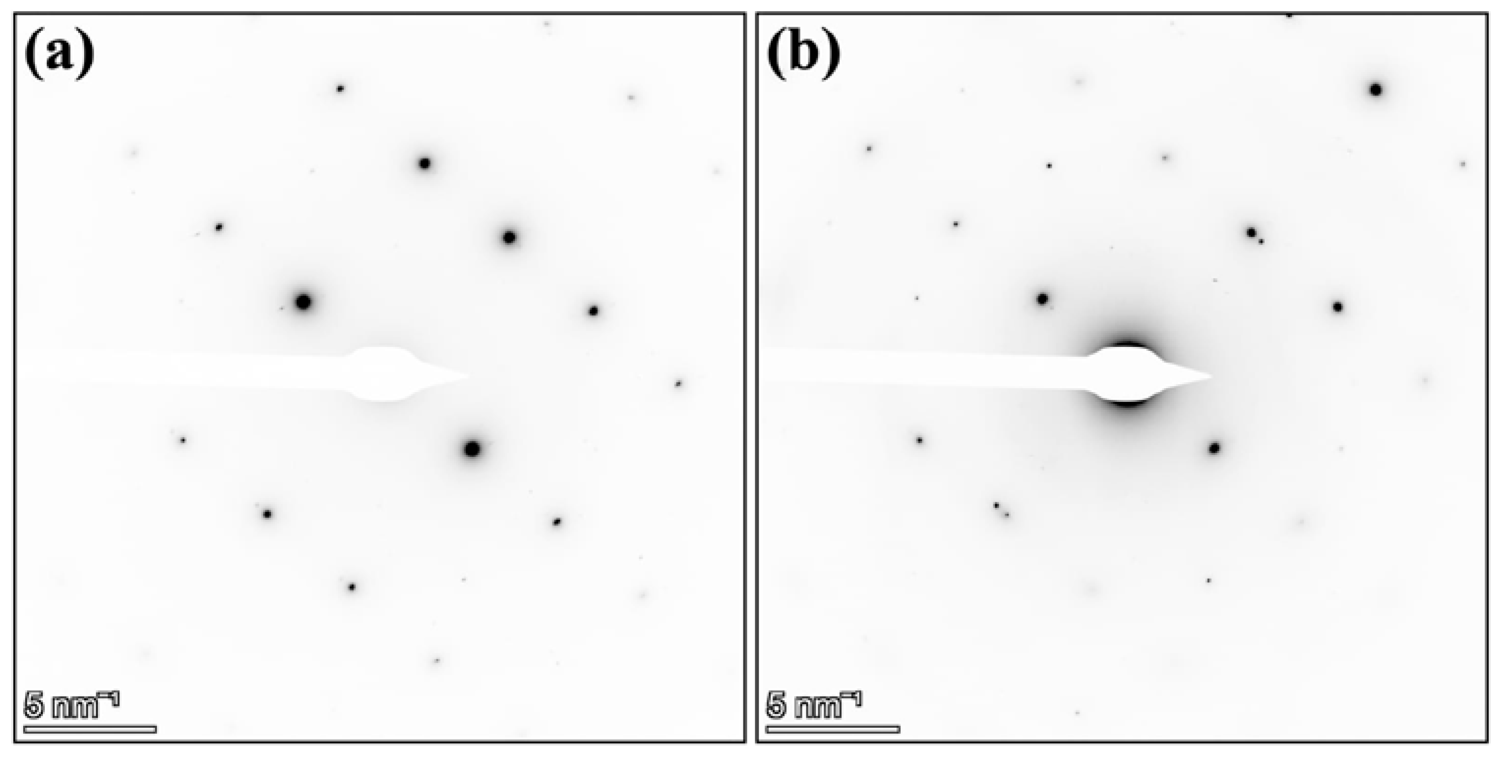
3.2. Characterisation with S/TEM
The electron-transparent piece attached to the MEMS e-chip as shown in
Figure 1i was loaded into the electron-microscope.
Figure 2a shows a BF-TEM micrograph taken at low-magnification indicating that the sample was stationary on the MEMS chip during both loading procedures into the holder and into the electron-microscope.
Figure 2a also indicates that the sample is covering four holes of the membrane of the MEMS e-chip. A high-magnification BF-TEM micrograph was taken from the hole indicated with a blue square in
Figure 2a: as shown in
Figure 2b, the sample is high-quality and electron-transparent, thus demonstrating the viability of the proposed sample preparation methodology.
It is worth emphasising that, when using the SEM-FIB for producing samples for MEMS e-chips, Pt is often deposited in specific areas of the sample in order to weld it onto the e-chip membrane [
2]. This step may introduce a significant yield of Pt contamination onto the surfaces of the electron-transparent specimen, which may compromise the MEMS experiments. The same is expected to occur upon interaction of either Ga or Xe ion beams with the metallic specimens during the stages of trenching, milling, cutting and polishing within the SEM-FIB. Conversely, in the several steps of the sample preparation methodology reported in this work neither Pt, Ga nor Xe are used; therefore, the sample will be free of those contaminants when compared to samples made within the SEM-FIB.
3.3. Paint Bake of AlMgZn(Cu) Alloy within a S/TEM
In order to evaluate both the quality and performance of the electron-transparent sample during a MEMS experiment a paint bake treatment was performed in situ in the STEM, which consisted of heating the AlMgZn(Cu) alloy up to 458 K for 1200 s. The LAADF micrograph in
Figure 3a shows the microstructure of the alloy prior to paint bake, which is composed of nanometer-sized Guinier–Preston zones (or simply GP Zones) and a high density of dislocations, given that the alloy was 2% deformed. Note that this is similar microstructure to that found in a conventionally produced AlMgZn(Cu) alloy [
18].
Upon paint bake, the microstructural evolution of the AlMgZn(Cu) alloy was monitored in real-time using the BF-STEM and LAADF detectors, the latter of which is shown in the micrographs in
Figure 3b–e, the former being reported in [
18]. A reorganization of the initial dislocation structure was observed to take place, including complete annihilation of pre-existing dislocations. During the experiment, the sample experienced minimal drift, only on the order of few nanometers, which was easily corrected manually with stage movement.
The SAED patterns shown in
Figure 4a,b exhibit the microstructure of the AlMgZn(Cu) alloy before and after the paint bake treatment. It is worth emphasising that the SAED patterns before and after the experiment do not show any Debye–Scherrer rings commonly associated with polycrystalline nanometer-sized artefacts introduced by Pt and Ga contamination when using samples produced via the SEM-FIB technique. As this is an experiment performed with an electron-transparent lamella at the nanoscale, the results may not correspond directly to those reported by Stemper, where heat treatment was performed in bulk specimens [
18].
3.4. Post-Experiment Impurity Analysis
STEM-EDX was used to analyse the elements present in the sample after the in situ STEM paint bake treatment.
Figure 5 shows a long-exposure (2 h) STEM-EDX raw spectrum collected from the whole area corresponding to the micrograph in
Figure 4b. The intensity axis (y-axis) of the STEM-EDX plot in
Figure 5 was set to logarithmic scale in order to better evaluate the presence of minor elemental peaks and a locally estimated scatterplot smoothing (LOESS) fit was used to better identify the peaks’ positions in the energy axis (x-axis). In order to define the relevance of a peak with respect to the background noise, the relative intensity of each identified peak was calculated against the strongest signal peak, e.g., the Al Kα peak index 7 located at 1.487 keV. Peaks with less than 0.01% of relative intensity were not considered.
Using this methodology, 20 peaks were identified in the STEM-EDX raw spectrum. The peaks’ indexes, as well as their energy and relative intensity, were extracted from the plot. The results are shown in
Table 1 and the accuracy of the STEM-EDX detector is noted. Most of the peaks are confirmed to have an energy match (with their expected position using reference values in the software Velox) in the third decimal place. Given such accuracy, the absence of contaminants such as Pt (Lα = 9.442 keV and Mα = 2.050 keV) and Ga (Kα = 9.251 keV and Lα = 1.098 keV) is remarkably noted. Minor impurities were identified as coming from the alloy production: Ca and Zr with extremely low relative intensity: 0.13% and 0.01% respectively. The presence of O is expected as Al self-passivates. Due to overlap between multiple different elements, the peaks corresponding to labels 3, 9, 10, 12, 17 and 18 were not properly identified, although their relative intensity is below 1%; therefore, we assume these impurities are from the inner microscope electronics, holder, e-chip or background noise.
The only contaminant observed with relative intensity of 1.6% was the element C (peak label 1). It is well known that EDX precludes the identification of the element C [
19], but the presence of this small peak can indeed be attributed to carbonaceous contamination either in the surface of the AlMgZn(Cu) sample or in the MEMS e-chip. However, this C contamination can be mitigated with the use of plasma cleaning, which was not applied in this work. Regardless of the minor C contamination and the presence of small impurities, the experiment and its outcomes were not in any way affected as confirmed by the detailed post-paint bake electron-microscopy analysis. No artefacts were observed to nucleate and grow on the alloy microstructure as a result of the experiment.
4. Conclusions
An alternative method for producing good-quality and implantation-free electron-transparent samples for MEMS experiments in situ within a S/TEM was introduced in this paper. The method consisted of using electropolished 3 mm disks from metallic samples with an electron-transparent hole in the center. The disk is then subjected to a set of precise cuts in order to separate the electron-transparent region into smaller pieces of around ≈50 µm. The electron-transparent piece can be transferred to pristine MEMS e-chips, with a high-quality animal hair used as a micrometer-sized manipulation tool.
The introduced methodology is faster than SEM-FIB and it allows the sample preparation of multiple samples from only one 3 mm electropolished disk. A paint bake experiment of an AlMgZn(Cu) alloy was performed in order to attest the quality of the sample and its stability during an in situ STEM experiment. Yield of minor impurities were observed to come from the Al alloy itself rather than the sample preparation method. The only minor extrinsic contamination observed was C, which is commonly identified when using the EDX technique for elemental estimation. None of the minor impurities nor C contamination were observed to affect the results of the paint bake experiment as no artefacts were observed to form and evolve in the sample.
This sample preparation methodology works well for both ductile and brittle metallic 3 mm electropolished disks, but it has not been yet tested for 3 mm dimpled and ion-polished ceramic discs.
Author Contributions
Conceptualization: S.P., C.R.Q., M.A.T. and P.D. Methodology: M.A.T., S.P. and C.R.Q. Valida-tion, C.R.Q., J.G., D.S.R.C., L.S. Formal analysis: M.A.T. and T.M.K. Investigation: M.A.T., T.M.K., D.S.R.C. and C.R.Q. Resources: L.S. Data curation: M.A.T. Writing—original draft preparation: M.A.T., C.R.Q. Writing—review and editing: S.P., M.A.T., C.R.Q., P.D., T.M.K., D.S.R.C., L.S. and J.G. Visualization: M.A.T., S.P., C.R.Q., T.M.K., D.S.R.C., P.D. Supervision: S.P. Project administra-tion: S.P. Funding acquisition: S.P. All authors have read and agreed to the published version of the manuscript.
Funding
The European Research Council (ERC) science grant “TRANSDESIGN” provided funding for the research reported in this work through the Horizon 2020 program under contract 757961. The electron-microscopy facility used in this work received funding from the Austrian Research Promotion Agency (FFG) project known as “3DnanoAnalytics” under contract number FFG-No. 858040.
Data Availability Statement
The raw/processed data required to reproduce these finding cannot be shared at this time as the data also forms part of an ongoing study.
Conflicts of Interest
The authors declare no conflict of interest.
References
- Noh, K.; Sun, L.; Chen, X.; Wen, J.; Dillon, S. In Situ TEM Characterization of Electrochemical Systems. Microsc. Microanal. 2011, 17, 1572–1573. [Google Scholar] [CrossRef] [Green Version]
- Zhong, X.L.; Schilling, S.; Zaluzec, N.J.; Burke, M.G. Sample Preparation Methodologies for In Situ Liquid and Gaseous Cell Analytical Transmission Electron Microscopy of Electropolished Specimens. Microsc. Microanal. 2016, 22, 1350–1359. [Google Scholar] [CrossRef] [PubMed] [Green Version]
- Damiano, J.; Nackashi, D.P.; Mick, S.E. A MEMS based Technology Platform for in-situ TEM Heating Studies. Microsc. Microanal. 2008, 14, 1332–1333. [Google Scholar] [CrossRef]
- Novák, L.; Stárek, J.; Vystavěl, T.; Mele, L. MEMS-based Heating Element for in-situ Dynamical Experiments on FIB/SEM Systems. Microsc. Microanal. 2016, 22, 184–185. [Google Scholar] [CrossRef] [Green Version]
- Hattar, K.; Han, J.; Saif, T.; Robertson, I.M. Development and Application of a MEMS-Based In Situ TEM Straining Device for Ultra-Fine Grained Metallic Systems. Microsc. Microanal. 2004, 10, 50–51. [Google Scholar] [CrossRef]
- Tochigi, E.; Sato, T.; Shibata, N.; Fujita, H.; Ikuhara, Y. In situ STEM Mechanical Experiments at Atomic-Resolution Using a MEMS Device. Microsc. Microanal. 2019, 25, 1884–1885. [Google Scholar] [CrossRef] [Green Version]
- Dillon, S.J.; Liu, Y. In-Situ TEM in Complex Environments: Photocatalysis. Microsc. Microanal. 2012, 18, 1072–1073. [Google Scholar] [CrossRef]
- Sun, L. In-situ TEM Study on Solar Cell. Microsc. Microanal. 2020, 26, 3160. [Google Scholar] [CrossRef]
- Li, W.; Li, M.; Wang, X.; Xu, P.; Yu, H.; Li, X. An in-situ TEM microreactor for real-time nanomorphology & physicochemical parameters interrelated characterization. Nano Today 2020, 35, 100932. [Google Scholar]
- Imrich, P.J.; Kirchlechner, C.; Kiener, D.; Dehm, G. In Situ TEM Microcompression of Single and Bicrystalline Samples: Insights and Limitations. JOM 2015, 67, 1704–1712. [Google Scholar] [CrossRef]
- Tuck, K.; Ellis, M.; Geisberger, A.; Skidmore, G.; Foster, P. FIB Prepared TEM Sample Lift-out Using MEMS Grippers. Microsc. Microanal. 2004, 10, 1144–1145. [Google Scholar] [CrossRef]
- Vijayan, S.; Jinschek, J.R.; Kujawa, S.; Greiser, J.; Aindow, M. Focused Ion Beam Preparation of Specimens for Micro-Electro-Mechanical System-based Transmission Electron Microscopy Heating Experiments. Microsc. Microanal. 2017, 23, 708–716. [Google Scholar] [CrossRef] [PubMed]
- Giannuzzi, L.A.; Stevie, F.A. A review of focused ion beam milling techniques for TEM specimen preparation. Micron 1999, 30, 197–204. [Google Scholar] [CrossRef]
- Mayer, J.; Giannuzzi, L.A.; Kamino, T.; Michael, J. TEM Sample Preparation and FIB-Induced Damage. MRS Bull. 2007, 32, 400–407. [Google Scholar] [CrossRef] [Green Version]
- Ernst, A.; Wei, M.; Aindow, M. A Comparison of Ga FIB and Xe-Plasma FIB of Complex Al Alloys. Microsc. Microanal. 2017, 23, 288–289. [Google Scholar] [CrossRef] [Green Version]
- Bender, H.; Franquet, A.; Drijbooms, C.; Parmentier, B.; Clarysse, T.; Vandervorst, W.; Kwakman, L. Surface contamination and electrical damage by focused ion beam: Conditions applicable to the extraction of TEM lamellae from nanoelectronic devices. Semicond. Sci. Technol. 2015, 30, 114015. [Google Scholar] [CrossRef]
- Estivill, R.; Audoit, G.; Barnes, J.-P.; Grenier, A.; Blavette, D. Preparation and Analysis of Atom Probe Tips by Xenon Focused Ion Beam Milling. Microsc. Microanal. 2016, 22, 576–582. [Google Scholar] [CrossRef] [PubMed]
- Stemper, L.; Tunes, M.A.; Dumitraschkewitz, P.; Mendez-Martin, F.; Tosone, R.; Marchand, D.; Curtin, W.A.; Uggowitzer, P.J.; Pogatscher, S. Giant hardening response in AlMgZn(Cu) alloys. Acta Mater. 2021, 206, 116617. [Google Scholar] [CrossRef]
- Isabell, T.C.; Fischione, P.E.; O’Keefe, C.; Guruz, M.U.; Dravid, V.P. Plasma Cleaning and Its Applications for Electron Microscopy. Microsc. Microanal. 1999, 5, 126–135. [Google Scholar] [CrossRef] [PubMed] [Green Version]
| Publisher’s Note: MDPI stays neutral with regard to jurisdictional claims in published maps and institutional affiliations. |
© 2021 by the authors. Licensee MDPI, Basel, Switzerland. This article is an open access article distributed under the terms and conditions of the Creative Commons Attribution (CC BY) license (http://creativecommons.org/licenses/by/4.0/).