Article

Performance Enhancement in N2 Plasma Modified AlGaN/AlN/GaN MOS-HEMT Using HfAlOX Gate Dielectric with Γ-Shaped Gate Engineering

Department of Electrical Engineering, Institute of Microelectronics, National Cheng Kung University, Tainan 701, Taiwan
*
Author to whom correspondence should be addressed.
These authors contributed equally to this work.
Materials 2021, 14(6), 1534; https://doi.org/10.3390/ma14061534
Submission received: 16 February 2021 / Revised: 11 March 2021 / Accepted: 19 March 2021 / Published: 21 March 2021

Abstract

:
In this paper, we have demonstrated the optimized device performance in the Γ-shaped gate AlGaN/AlN/GaN metal oxide semiconductor high electron mobility transistor (MOS-HEMT) by incorporating aluminum into atomic layer deposited (ALD) HfO2 and comparing it with the commonly used HfO2 gate dielectric with the N2 surface plasma treatment. The inclusion of Al in the HfO2 increased the crystalline temperature (~1000 °C) of hafnium aluminate (HfAlOX) and kept the material in the amorphous stage even at very high annealing temperature (>800 °C), which subsequently improved the device performance. The gate leakage current (IG) was significantly reduced with the increasing post deposition annealing (PDA) temperature from 300 to 600 °C in HfAlOX-based MOS-HEMT, compared to the HfO2-based device. In comparison with HfO2 gate dielectric, the interface state density (Dit) can be reduced significantly using HfAlOX due to the effective passivation of the dangling bond. The greater band offset of the HfAlOX than HfO2 reduces the tunneling current through the gate dielectric at room temperature (RT), which resulted in the lower IG in Γ-gate HfAlOX MOS-HEMT. Moreover, IG was reduced more than one order of magnitude in HfAlOX MOS-HEMT by the N2 surface plasma treatment, due to reduction of N2 vacancies which were created by ICP dry etching. The N2 plasma treated Γ-shaped gate HfAlOX-based MOS-HEMT exhibited a decent performance with IDMAX of 870 mA/mm, GMMAX of 118 mS/mm, threshold voltage (VTH) of −3.55 V, higher ION/IOFF ratio of approximately 1.8 × 10⁹, subthreshold slope (SS) of 90 mV/dec, and a high VBR of 195 V with reduced gate leakage current of 1.3 × 10⁻¹⁰ A/mm.

1. Introduction

In recent years, the wide band gap semiconductors have been widely used in high power electronic applications due to its high power density and high power conversion efficiency [1]. As of today, the AlGaN/GaN based high electron mobility transistors (HEMTs) are the most promising devices for high power and high frequency applications due to their unique properties such as wide band gap (3.4 eV of GaN), large breakdown field (>3 MV/cm), high density of two-dimensional electron gas (2 DEG) (~1013/cm2), low intrinsic carrier density, and high saturation velocity (~ 2 × 10 7 / cm 2 ) [2,3,4,5]. Due to the safety and power saving concerns, the recessed gate GaN-based HEMTs are desirable to realize the normally-off operation [6]. However, Ki-Sik et al. and Zhe at al. reported that the electron transport characteristics could be seriously affected by the interface states in fully recessed HEMTs, due to the completely etched AlGaN barrier layer [7,8].
In order to avoid the degradation of the transport characteristics of the carrier the partially recessed GaN HEMT structure was proposed [9]. The Cl2-based inductive coupled plasma (ICP) dry etching has been widely used, to realize the partially recessed-gate structure. However, the gate recess process induced the trap states in the device, leading to the severe gate leakage, worse current collapse, and very low breakdown voltage (VBR) [6,10]. Baik et al. reported that the N2 plasma treatment could effectively improve the surface morphology and ohmic contacts in GaN HEMTs by reducing the N2 vacancies, created by ICP dry etching [11].
In addition to the N2 surface treatment, to reduce the gate leakage current significantly, the metal oxide semiconductor high electron mobility transistor (MOS-HEMT) with an insulating dielectric have also been widely investigated. Numerous gate dielectrics have been experimented, such as SiO2 [12], AlN [13], Al2O3 [14], MgCaO [15], HfO2 [16], ZrO2 [17], TiO2 [18], etc. The dielectric layer not only can suppress the gate leakage current, but also can be used as a passivation layer to suppress the current collapse phenomenon [19]. Among the many used dielectrics, HfO2-based MOS-HEMTs can achieve much more efficient electrostatic control due to their high dielectric constant (k). However, due to the insufficient barrier height, the HfO2-based GaN MOS-HEMT suffers from a high gate leakage current, which subsequently deteriorates the device performance [20]. Thus, to reduce the gate leakage current without the reduction of gate controllability, the HfO2-based stack gate dielectric layer such as HfO2/Y2O3 [21], HfO2/Al2O3 [16], HfO2/AlN [22] or Hf-ternary oxide HfSiOX [20], HfZrO [23], etc. have also been investigated. However, owing to the lower crystalline temperature, e.g., Y2O3 (~ <425 °C) [24] and HfZrO (500~550 °C) [25], the respective MOS-HEMT might not be applicable in a high temperature.
A previous study has shown that the inclusion of Al into HfO2 could improve the interface properties and reduce the gate leakage current in hafnium aluminate (HfAlOX)-based MOS-HEMTs [26,27]. HfO2 provides a high dielectric constant (k ~ 25) but poor conduction band offset to GaN (~1.51 eV), while Al2O3 offers a larger conduction band offset to GaN (~1.96 eV) but it has a relatively lower dielectric constant (k ~ 9) [27]. To improve the channel controllability a high-k material is preferred, whereas a large conduction band offset is required to reduce the gate leakage current.
In addition, a high temperature sustainability is much more important for a high power application. Since the phase change from amorphous to crystalline will rise to the leakage current, the crystalline temperature of HfO2 (~400 °C) is much lower than Al2O3 (~900 °C) [27]. Previous reports also suggested that the HfO2 suffers severely from the interface state and border state densities than Al2O3, which affects the device performances significantly [26,28]. Thus, by incorporation of Al into HfO2 the thermal stability of the ternary compound, i.e., HfAlOX could be improved significantly.
The crystallization temperature of HfAlOX could give rise to ~1000 °C with 45.5% of Al [26]. The conduction band offset of HfAlOX is also much higher (~1.61 eV) [27], with a high dielectric constant (k~14) [29]. Moreover, due to the incorporation of Al, the interface state density is effectively reduced with the passivation of the dangling bond in HfAlOX, which helps the improvement in the device performance significantly [30]. To date, the direct observation of the enhancement of device performance in HfAlOX-based MOS-HEMTs with N2 surface plasma alteration using the Γ - shaped gate structure, has not yet been investigated.
With this aim in mind, in this work, we have demonstrated the improvement of device performance in Γ - gate AlGaN/AlN/GaN MOS-HEMT with the Al doped HfO2 gate dielectric and N2 surface plasma modulation. The inclusion of Al into HfO2 increased the crystalline temperature of HfAlOX, which reduced the gate leakage current at a high PDA temperature (~600 °C). The interface state density of HfAlOX MOS-HEMT is reduced nearly one order of magnitude, which improved the hysteresis behaviour of the device. Moreover, the use of gate field plate (FP) increased the breakdown voltage (VBR ) of the device. The N2 plasma treated Γ -shaped gate HfAlOX-based MOS-HEMT exhibited a decent performance with IDMAX of 870 mA/mm, GMMAX of 118 mS/mm, threshold voltage (VTH) of −3.55 V, higher ION/IOFF ratio of approximately 1.8 × 10 9 , subthreshold slope (SS) of 90 mV/dec, and a VBR of 195 V with the reduced gate leakage current of 1.3 × 10 10 A/mm.

2. Materials and Methods

The AlGaN/AlN/GaN-epitaxy was grown on a 6-inch low resistive (111) Si substrate by the metal organic chemical vapour deposition (MOCVD) system. The epitaxial layer consists of a 5.5 μm GaN buffer layer, a 200 nm GaN channel layer, a 1 nm AlN layer and a 25 nm Al0.23Ga0.77N barrier layer, and a 2 nm GaN cap layer. The measured Hall mobility, sheet carrier concentration, and sheet resistance were found to be 1800 cm2/V·s, 8 × 1012 cm−2, and 434 Ω/◻, respectively.
To achieve the device isolation the mesa etching was employed by using the inductive coupled plasma reactive ion etching (ICP-RIE) system under the Cl2/BCl3 environment. After that, the source and drain regions were defined using UV-photolithography, followed by Ti/Al/Ni/Au (25/150/30/120 nm) metal stacks were deposited by the electron beam (e-beam) evaporation system. Then, the rapid thermal annealing (RTA) took place at 875 °C for 45 s in N2 ambient to ensure the good ohmic contact. After that, the gate recess area was defined by the ELS-7500 EX electron beam lithography (EBL) system. Subsequently, the GaN and AlGaN layers under the gate were partially recessed while using low power ICP-RIE. After that, the N2 plasma treatment was done by RF-sputter and the sample was transferred to the atomic layer deposition (ALD) chamber (Picosun) to deposit the gate dielectric. The 10 nm thick hafnium aluminate (HfAlOX) was deposited as the gate dielectric by ALD at 250 °C. As for the 10 nm HfAlOX deposition, three cycles of Al2O3 were first deposited, then four cycles of HfO2, and one cycle of Al2O3 were cyclically deposited until the total thickness of 10 nm. Then, the sample was coated with an electron resist and baked at 180 °C for 7.5 min. After that, the Γ -shaped gate region was defined by the e-beam lithography system. Finally, the Ni/Au (80/100 nm) gate metal stack was deposited by the e-gun evaporator. In addition, (i) the Γ -shaped gate MOS-HEMT with the HfO2 gate dielectric, (ii)   Γ -shaped gate HEMT, and (iii) non-recessed HEMT (C-HEMT) were also fabricated following the same process as the control samples. In addition, to examine the high temperature sustainability of HfAlOX, the MOS-HEMTs were fabricated with three different post deposition annealing (PDA) temperatures, i.e., 300, 600, and 800 °C for 1 min, and compared with HfO2 MOS-HEMT. The schematic of the AlGaN/AlN/GaN Γ -shaped gate MOS-HEMT is shown in Figure 1a. All the devices were fabricated with the same gate length (LG = 0.5 µm) and LGD/LSD (2/2 µm).

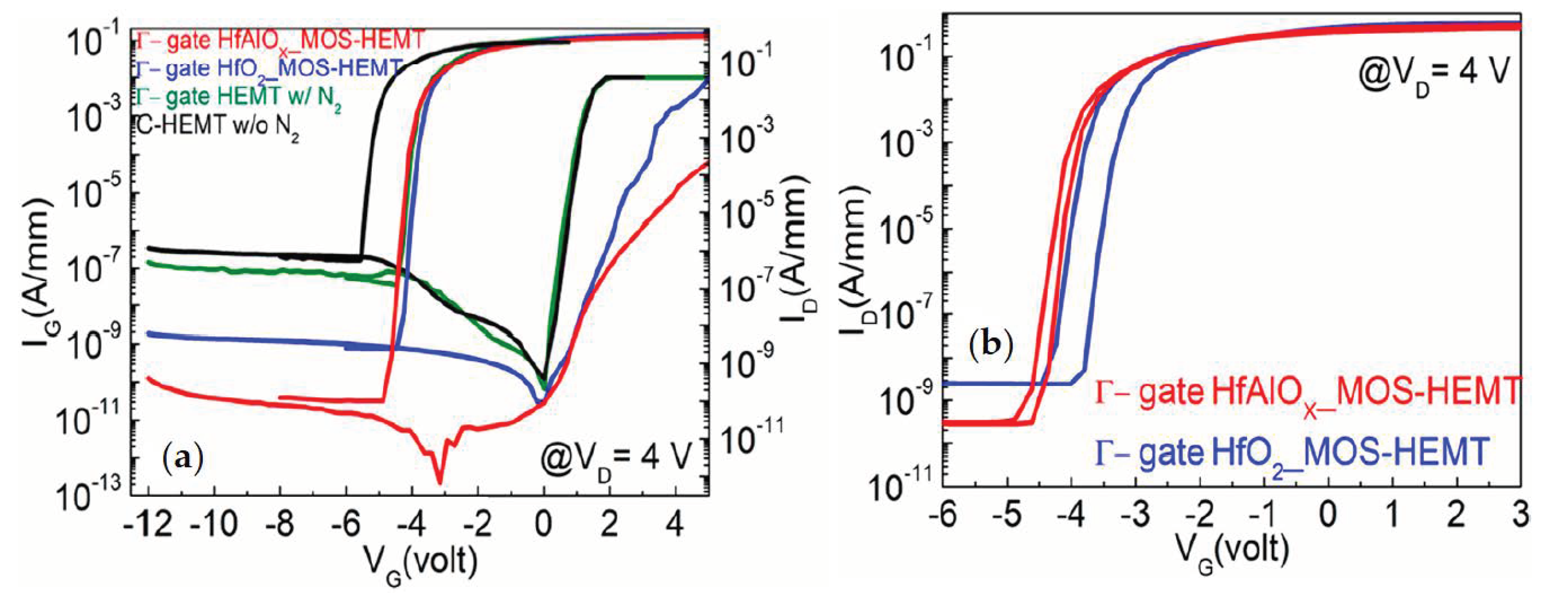
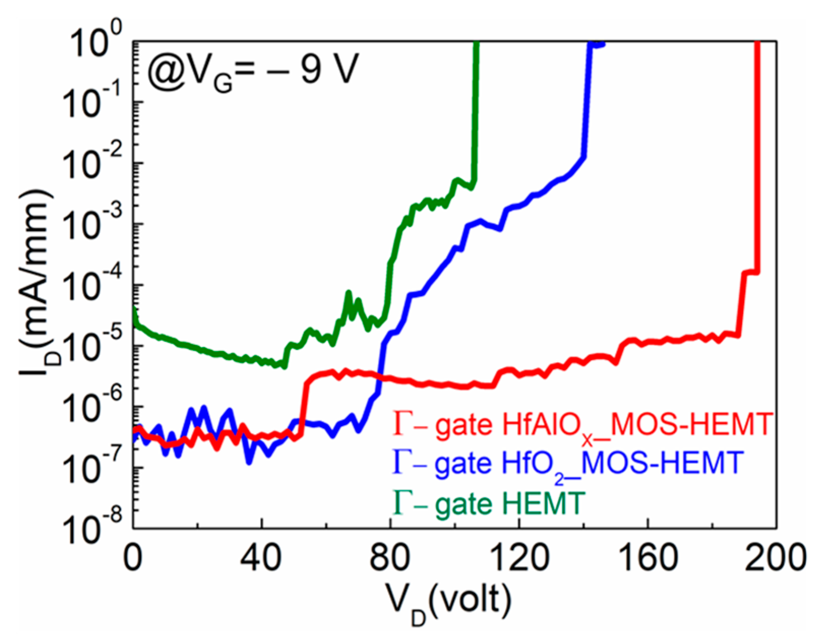
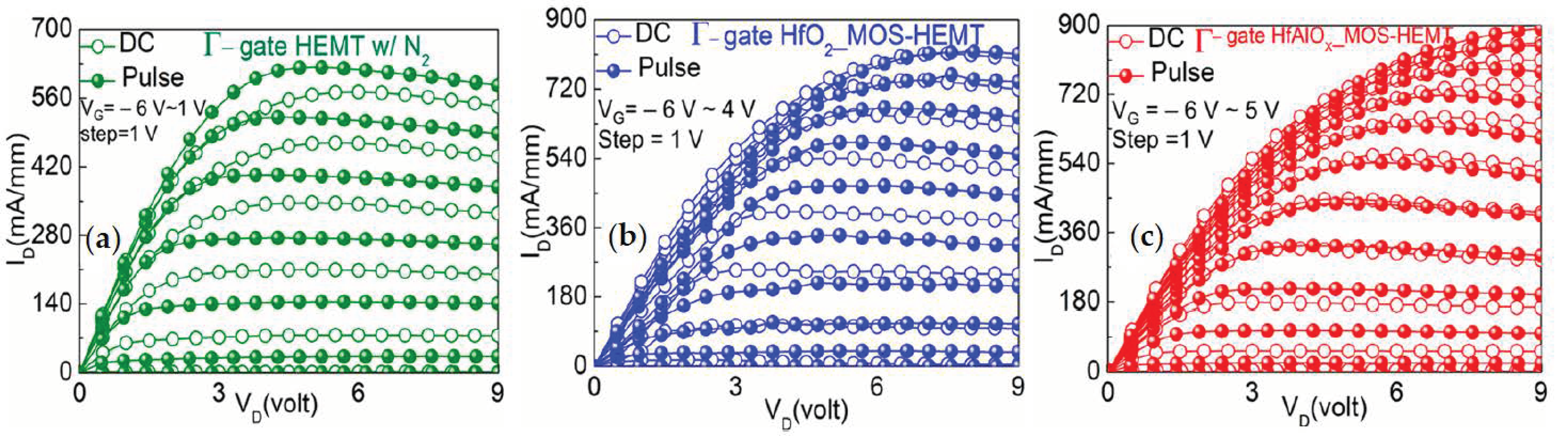
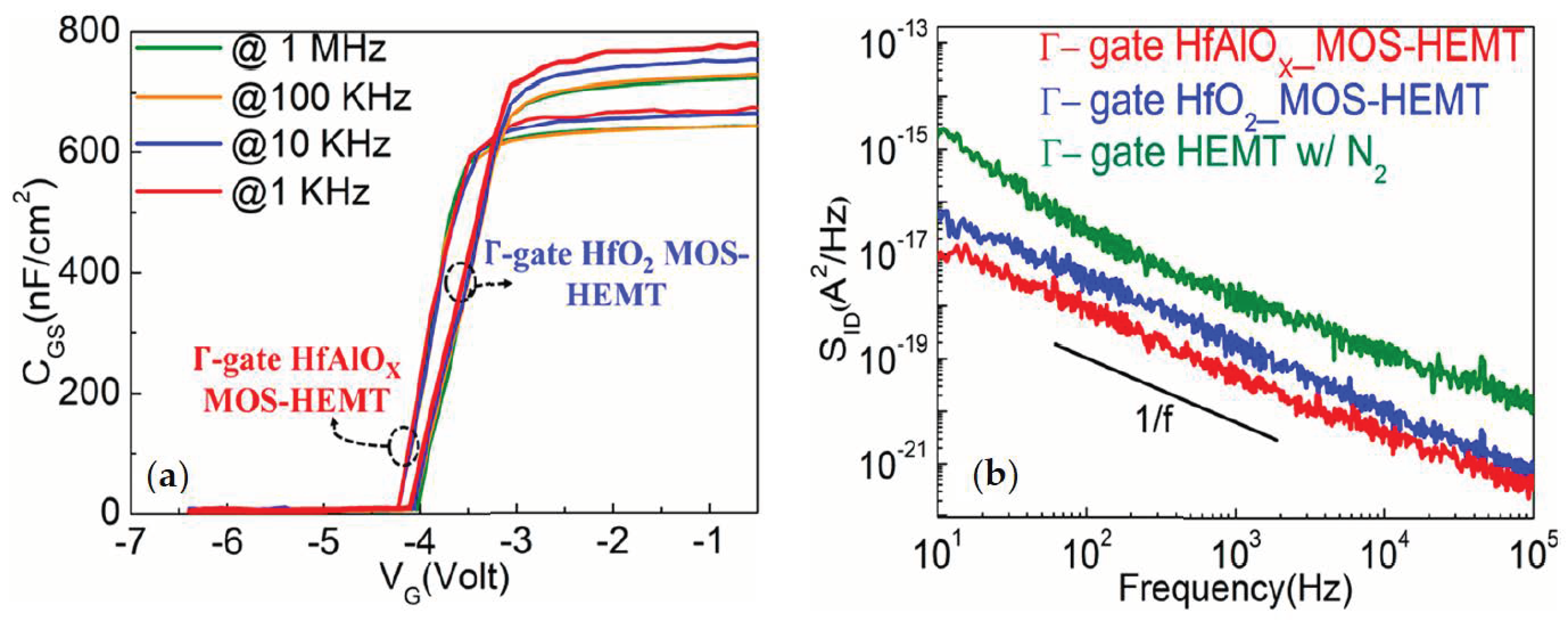
3. Results and Discussion

Figure 1b–i shows the typical transmission electron microscope (TEM, JEM-2010 Electron Microscope; JEOL Co. 200 KV) images of the HfO2- and HfAlOX-based MOS-HEMT. Without the intermixing of layers, a quite smooth oxide/GaN interface was observed. In order to compare the thermal stability of HfO2 and HfAlOX, the PDA was done at 300 °C and 600 °C for 1 min and the characteristics were analyzed. Figure 1b,c shows the TEM images of the   Γ -gate HfO2 and HfAlOX MOS-HEMTs with the PDA at 300 °C. It was noticed that the gate dielectrics were in amorphous stage, i.e., no crystalline lattice fringes were found after the PDA at 300 °C. From Figure 1d, it can be observed that the amorphous phase of HfO2 was changed to polycrystalline with the increasing annealing temperature from 300 to 600 °C. In addition, the selected area diffraction pattern (SADP) was used to analyze the details of the crystal diffraction by TEM, as shown in Figure 1e. Some diffraction peaks were found in the 600 °C annealed HfO2 MOS-HEMT. As the AlGaN is a single crystal, thus, the diffraction ring is about the HfO2 crystallization.
On the other hand, from Figure 1f,g it can be clearly understood that the HfAlOX was still in the amorphous stage at 600 °C. No diffraction peak was found in the SADP image, which further proved the aforementioned statement. In order to further analyze the thermal stability of HfAlOX, the material was annealed at 800 °C for 1 min. The TEM and SADF images proved that HfAlOX was still amorphous, as shown in Figure 1h,i. The results revealed that the crystallization temperature of HfO2 was improved to a great extent by the incorporation of Al. Figure 1j shows the energy-dispersive X-ray spectroscopy (EDX) measurement with a line scan mode of HfAlOX film. It can be observed that the Hf and Al atoms are distributed uniformly. The ratio between Al and Hf in HfAlOX is about 1:2.
Figure 2a,b shows the gate leakage (IG) characteristics of HfO2- and HfAlOX-based MOS-HEMTs with different PDA temperatures. The gate leakage current of HfO2 MOS-HEMT was increased approximately two orders of magnitude with the increasing annealing temperature to 600 °C, as shown in Figure 2a. As the TEM images confirmed that the HfO2 phase changes from amorphous to polycrystalline with the increasing PDA temperature, thus the additional high leakage path along the grain boundaries through the poly crystalline dielectrics increased IG with the PDA temperature [26]. The IG values (@ VG = −12 V) were found to be approximately 10−7 and 10−8 A/mm (10−9 A/mm) orders of magnitude for Γ -gate HfO2 MOS-HEMTs with 600 and 300 °C PDA (w/o PDA). From Figure 2b, it can be observed that the IG values were decreased about two orders of magnitude with the increasing annealing temperature from 300 to 600 °C in HfAlOX MOS-HEMTs. The decreased trap density with the increasing annealing temperature might be one possible reason for the reduction in the leakage current [26]. The IG (@ VG = −12 V) was increased from 10−9 to 10−8 mA/mm, when the temperature raised from room temperature (RT) to 300 °C, and then the gate leakage was reduced approximately to 10−10 mA/mm, with further increments of the PDA temperature to 600 °C. At a higher temperature, the growth of SiO2 at the interface resulted in the reduction in IG [26].
In order to analyze the effects of nitrogen (N2) plasma treatment after ICP etching, on the gate leakage current, the IG–VG characteristics were calibrated from Γ -gate HEMT and HfAlOX MOS-HEMTs with and without the N2 plasma treatment, as shown in Figure 3a,b. It can be clearly observed that the gate leakage current was reduced more than one order of magnitude in Γ -gate HfAlOX MOS-HEMTs, whereas the IG was reduced approximately two orders of magnitude in the Γ -gate partially recessed HEMT by the N2 plasma treatment. The N2 vacancies, created by ICP dry etching, could be filled by the nitrogen radicals generated from the pure N2 plasma. In addition, reducing the dangling bonds by forming Ga-N bonds resulted in activating the surface, which correspondingly reduced the gate leakage current [31].
The typical drain current-voltage characteristics of the Γ -gate HEMT-, HfO2-, HfAlOX-based MOS-HEMT, and non-recessed HEMT is shown in Figure 4. The maximum drain currents (IDMAX) of the HfAlOX- (@VG = 5 V) and HfO2- (@VG = 4 V) based MOS-HEMTs were found to be 870 and 775 mA/mm, respectively. Whereas, IDMAX values (@VG = 1 V) were found to be 570 and 520 mA/mm for the recessed and non-recessed HEMT, respectively, which is comparatively much lower than Γ -gate MOS-HEMT. Owing to the large gate leakage current, the HEMTs were not biased with the high gate voltage [32]. Henceforth, due to the insertion of the gate dielectrics the gate leakage current can be effectively suppressed, which resulted in the improvement of the IDMAX in the MOS-HEMT.
To understand the gate controllability of the N2-plasma treated Γ -gate HEMT-, HfO2-, and HfAlOX-based MOS-HEMT and C-HEMT, the transfer characteristics were calibrated at VD = 4 V, as shown in Figure 5. The threshold voltage (VTH) is defined as the gate bias intercept point of the linear extrapolation of ID at peak transconductance (GMMAX) [33]. The threshold voltages were found to be −3.55, −3.41, and −3.55 V for Γ -gate HEMT-, HfO2-, and HfAlOX-based MOS-HEMT, respectively. In comparison, the VTH of the non-recessed HEMT was found to be −4.9 V. The partially gate recessed and the use of field plate structure resulted in the positive shifting of VTH in   Γ -gate HEMT and MOS-HEMTs. The maximum transconductances were found to be 139, 116, and 118 mS/mm for the partially recessed HEMT-, HfO2-, and HfAlOX-based MOS-HEMT, respectively. The insertion of the gate dielectric layer, increased the distance between the gate and 2DEG channel. Therefore, the controllability of the gate is decreased which resulted in the reduction of the transconductance. The GMMAX was found to be 114 mS/mm for the non-recessed HEMT.
Figure 6a shows the subthreshold characteristics as a function of the gate voltage (@ VD = 4 V) for Γ -gate HEMT-, HfO2-, and HfAlOX-based MOS-HEMT with the N2-plasma treatment, and non-recessed HEMT. From Figure 6a, it is clearly observed that the subthreshold drain leakage current was decreased more than two orders of magnitude in the HfAlOX-based MOS-HEMT, than the Γ -shaped gate HEMT. The HfAlOX gate dielectric improved the metal/semiconductor junction which subsequently reduced the drain leakage current. The subthreshold drain leakage current is dominated by the reverse biased gate leakage current (IG) in the off-state [34]. Thus, the reduction of the reverse biased gate leakage current in the MOS-HEMT, resulted in the decrement of the subthreshold drain leakage current, as shown in Figure 6a.
The subthreshold swing (SS) also depends on the IG. To understand the gate controllability, the SS values were extracted for different devices from Figure 6a. The SS values were found to be 101, 86, and 90 mV/dec for the N2-plasma treated partially recessed HEMT-, HfO2-, and HfAlOX-based MOS-HEMT, respectively. The current ON/OFF ratio (ION/IOFF) of the aforementioned devices were found to be 2.9 ×   10 6 , 2.3 ×   10 8 , and 1.8 ×   10 9 , respectively. The SS and ION/IOFF were found to be 110 mV/dec and 1.04 ×   10 6 , respectively for the non-recessed HEMT.
The reduction of the off-state gate leakage current is important in GaN HEMTs for their application in the electrical circuit. In general, it is also important to achieve a low flicker noise and low power consumption. The reversed and forward gate leakage I-V characteristics of the N2-plasma treated Γ -gate HEMT-, HfO2-, and HfAlOX-based MOS-HEMT and C-HEMT are shown in Figure 6a. It is clearly revealed that the reverse biased gate leakage current of Γ -gate MOS-HEMT was reduced more than two orders of magnitude than the Γ -gate or non-recessed HEMT due to the insertion of gate oxide as expected. The reversed biased gate leakage current (@ VG = −12 V) were found to be 1.5 × 10 7 , 1.7 × 10 9 , and, 1.3 × 10 10 A/mm for the N2-plasma treated Γ -gate HEMT-, HfO2-, HfAlOX-based MOS-HEMT. In particular, the HfAlOX-based device exhibited the lowest IG among all the devices. Due to the inclusion of Al in HfO2, the band gap increased from ~ 5.8 eV to greater than 6.5 eV for HfAlOX with ~50% of Al, which is consistent with the large band gap of Al2O3 (~8.1 eV) [26]. The greater band offset of the HfAlOX than HfO2, effectively reduced the tunneling current which results in the reduction of the gate leakage current [26]. It can also be noted that the forward leakage current (@ VG = 5 V) also reduced more than three orders of magnitude in the HfAlOX-based MOS-HEMT than the other devices, due to the large band offset. In comparison with the other devices, for C-HEMT without FP and the N2 surface treatment, the IG was found to be approximately (@ VG = −12 V) 3.7 × 10 7 A/mm.
To understand the hysteresis behavior of the gate dielectrics, the double sweep subthreshold transfer characteristics of Γ -gate HfO2 and HfAlOX MOS-HEMT were measured, as shown in Figure 6b. It is clearly seen that the HfAlOX-based MOS-HEMT (~150 mV) exhibited a much smaller hysteresis than the HfO2-based devices (~484 mV). With the inclusion of Al into HfO2 the interface state density was reduced due to the effective passivation of the dangling bonds in HfAlOX than HfO2 [30]. The incorporation of Al into HfO2 also reduced the border traps which resulted in the reduction of hysteresis in HfAlOX [26].
The off-state breakdown characteristics of different devices is shown in Figure 7. The breakdown voltages were found to be 107, 145, and 195 V for the Γ -gate HEMT-, HfO2-, and HfAlOX-based MOS-HEMT, respectively. The defect states caused by ICP dry etching increased the gate leakage, resulting in the significant reduction of the breakdown voltage (VBR) in the Γ -gate HEMT. As discussed earlier, due to the inclusion of Al into HfO2 the Γ -gate/HfAlOX interface was improved with a greater dangling bond passivation with the increased band gap and reduced IG, which resulted in a much higher VBR in the HfAlOX- based MOS-HEMT compared to the HfO2-based device.
The current collapse is an important issue for the electrical performance of AlGaN/GaN HEMTs, due to the electron trapping at the AlGaN surface states between the gate and the drain the current collapse occurred [31]. To investigate the effectiveness of the HfAlOX gate dielectric with the field plate structure on the current degradation, the gate lag measurements were employed. Figure 8a–c shows the drain current response of the Γ -gate HEMT-, HfO2-, and HfAlOX-based MOS-HEMT with the field plate structure. The pulse width is 500 μs and the pulse period is 50 ms. From the observations, it was clearly revealed that the current collapse phenomenon was effectively suppressed with the gate dielectric in the partially recessed MOS-HEMT. The drain-source current collapse was improved in the HfAlOX-based MOS-HEMT to 4% (@VD = 8 V, VG = 0 V), while for the HfO2-based MOS-HEMT and partially-recessed HEMT it was found to be approximately 13% and 18%, respectively. Most of the surface states presented at the source-drain access regions might have been passivated with the combined effects of the N2 plasma treatment and HfAlOX surface passivation with the application of the gate field plate.
In order to understand the reduction of trap states of Γ - gate HfO2 and HfAlOX-based MOS-HEMTs, the capacitance-voltage (C-V) measurements were done for the devices at different frequencies, as shown in Figure 9a. The interface state densities (Dit) were extracted from the previously reported formula [35] to be 1.8 × 10 12 and 7.1 ×   10 12   eV 1 · cm 2 for the HfAlOX- and HfO2-based MOS-HEMTs, respectively. In addition, the interface quality between the gate dielectric and the GaN layer could also be evaluated from the frequency dependent C-V measurement shown in Figure 9a. The interval of the C-V curve improved to 60 mV from 130 mV for the HfAlOX device, indicating the excellent interface quality between the gate dielectric and GaN layer [36,37].
Low-frequency noise measurements are an effective method for studying the electron trapping and de-trapping behaviour. Figure 9b shows the low-frequency noise characteristics, measured at VDS = 2.9 V and VGS = −3.9 V, with frequencies ranging from 10 to 100 kHz, for the Γ -gate HEMT-, HfO2-, and HfAlOX-based MOS-HEMT. In the noise characteristics, the variation of noise current density SID (A2/Hz) with the frequency was measured. The 1/f-noise characteristics are directly related to the presence of the electron trap and de-trapping between the 2DEG channels and the traps presented in the GaN buffer layer [38]. It was observed that SID of the Γ -gate MOS-HEMT was more than one order lower than the partially recessed HEMT. The gate dielectrics significantly reduced the gate leakage currents and passivated the S/D access region, which subsequently improved the interface quality, as discussed earlier. Consequently, the insertion of gate dielectric layer can suppress the flicker noise. In particular, due to the better interface quality with the lower interface density, the noise current density was found one order lower in HfAlOX-based MOS-HEMT (~10−17 A2/Hz) than the HfO2-based device (10−16 A2/Hz) at a low frequency. Table 1 shows the comparison of the N2 plasma treated Γ - gate HEMT-, HfO2-, HfAlOX-based MOS-HEMT and non-recessed HEMT. Table 2 shows the comparison of electrical performances of   Γ -gate HfAlOX-based MOS-HEMT with different Al2O3 and HfO2-based MOS-HEMTs. The performance is comparable with the previous reports.

4. Conclusions

In summary, we have demonstrated the comparative study of N2 plasma treated Γ - shaped gate AlGaN/AlN/GaN MOS-HEMT with HfO2 and HfAlOX as gate dielectrics. The off-state gate leakage current was significantly reduced with the increasing PDA temperature from 300 to 600 °C in the HfAlOX-based MOS-HEMT compared to the HfO2-based devices. Due to the inclusion of Al into HfO2, the crystallization temperature was significantly improved to ~1000 °C of HfAlOX. Moreover, due to the higher conduction band offset of HfAlOX to GaN (~1.61 eV), the gate leakage current was effectively reduced in HfAlOX MOS-HEMT even at the higher temperature. The interface state density (Dit) in the HfAlOX-based MOS-HEMT was effectively reduced compared to the HfO2 device, due to the effective passivation of the dangling bonds, which subsequently improved the hysteresis and current collapse characteristics. Due to the reduction of N2 vacancies, created by ICP dry etching, the gate leakage current was reduced more than one order of magnitude by the N2 surface plasma treatment. The Dit values were improved to 1.8 × 10 12 eV 1 · cm 2 from 7.1 × 10 12   eV 1 · cm 2 for HfAlOX MOS-HEMT than HfO2 MOS-HEMT. The N2 plasma treated Γ -shaped gate HfAlOX MOS-HEMT exhibited a decent performance with IDMAX of 870 mA/mm, GMMAX of 118 mS/mm, threshold voltage (VTH) of −3.55 V, higher ION/IOFF ratio of approximately 1.8 × 10 9 , subthreshold slope (SS) of 90 mV/dec, a VBR of 195 V with reduced current collapse of 4%, and gate leakage current of 1.3 × 10 10 A/mm.

Author Contributions

Device preparation and characterization, S.-K.Y.; characterization, data analysis and writing of the paper, S.M.; data analysis and manuscript revision, S.-K.Y., S.M., Z.-G.W. and Y.-H.W.; monitoring the progress of the paper and editing, Y.-H.W. All authors have read and agreed to the published version of the manuscript.

Funding

This research was funded by the Ministry of Science and Technology, Taiwan, grant numbers MOST 106-2221-E-006-219-MY3 and MOST 109-2221-E-06-075-MY2 and Transcom. Inc., Taiwan, grant number 109S0172.

Institutional Review Board Statement

Not applicable.

Informed Consent Statement

Not applicable.

Data Availability Statement

The data presented in this study are available on request from the corresponding author.

Acknowledgments

The flicker noise measurements in the Taiwan Semiconductor Research Institute, National Applied Research Laboratories, Taiwan are highly appreciated.

Conflicts of Interest

The authors declare no conflict of interest.

References

  1. Hu, J.; Zhang, Y.; Sun, M.; Piedra, D.; Chowdhury, N.; Palacios, T. Materials and processing issues in vertical GaN power electronics. Mater. Sci. Semicond. Process. 2018, 78, 75–84. [Google Scholar] [CrossRef] [Green Version]
  2. Ardaravičius, L.; Matulionis, A.; Liberis, J.; Kiprijanovic, O.; Ramonas, M.; Eastman, L.F.; Shealy, J.R.; Vertiatchikh, A. Electron drift velocity in AlGaN/GaN channel at high electric fields. Appl. Phys. Lett. 2003, 83, 4038–4040. [Google Scholar] [CrossRef]
  3. Basu, S.; Singh, P.K.; Sze, P.W.; Wang, Y.H. AlGaN/GaN Metal oxide-semiconductor high electron mobility transistor with liquid phase deposited Al2O3 as gate dielectric. J. Electrochem. Soc. 2010, 157, 947–951. [Google Scholar] [CrossRef]
  4. Borga, M.; Meneghini, M.; Benazzi, D.; Canato, E.; Püsche, R.; Derluyn, J.; Abid, I.; Medjdoub, F.; Meneghessoa, G.; Zanoni, E. Buffer breakdown in GaN-on-Si HEMTs: A comprehensive study based on a sequential growth experiment. Microelectron. Reliab. 2019, 100, 1–5. [Google Scholar] [CrossRef]
  5. Mazumder, S.; Wang, Y.H. Investigation of HfSiOX Passivation Effect on AlGaN/GaN HEMT. In Proceedings of the 2020 International Symposium on Devices, Circuits and Systems (ISDCS), Howrah, India, 4–6 March 2020; pp. 1–4. [Google Scholar]
  6. Jun, L.; Zhao, S.L.; Mi, M.H.; Hou, B.; Yang, X.L.; Zhang, J.C.; Ma, X.H.; Hao, Y. Trap states induced by reactive ion etching in AlGaN/GaN high-electron-mobility transistors. Chin. Phys. B 2015, 24, 117305. [Google Scholar]
  7. Im, K.S.; Ha, J.B.; Kim, K.W.; Lee, J.S.; Kim, D.S.; Choi, H.C.; Lee, J.H. AlGaN/GaN-based normally-off GaN MOSFET with stress controlled 2DEG source and drain. Phys. Status Solidi 2010, 7, 2013–2015. [Google Scholar] [CrossRef]
  8. Xu, Z.; Wang, J.; Cai, Y.; Liu, J.; Jin, C.; Yang, Z.; Wang, M.; Yu, M.; Xie, B.; Wu, W.; et al. Enhancement mode (E-Mode) AlGaN/GaN MOSFET with 10−13 A/mm leakage current and 1012 ON/ OFF current ratio. IEEE Electron Device Lett. 2014, 35, 1200–1202. [Google Scholar] [CrossRef]
  9. Han, K.; Zhu, L. GaN MOSHEMT employing HfO2 as a gate dielectric with partially etched barrier. Semicond. Sci. Technol. 2017, 32, 095004. [Google Scholar] [CrossRef]
  10. Adak, S.; Swain, S.K.; Singh, A.; Pardeshi, H.; Pati, S.K.; Sarkar, C.K. Study of HfAlO/AlGaN/GaN MOS-HEMT with source field plate structure for improved breakdown voltage. Phys. E 2014, 64, 152–157. [Google Scholar] [CrossRef]
  11. Min, B.J.; Yoon, S.; Won, K.T.; Lam, L.J. Enhancement of magnetic properties in (Ga,Mn)N nanowires due to plasma treatment. Appl. Phys. Lett. 2006, 89, 152113. [Google Scholar]
  12. Mazumder, S.; Li, S.H.; Wu, Z.G.; Wang, Y.H. Combined Implications of UV/O3 Interface Modulation with HfSiOX Surface Passivation on AlGaN/AlN/GaN MOS-HEMT. Crystals 2021, 11, 136. [Google Scholar] [CrossRef]
  13. Tsurumi, N.; Ueno, H.; Murata, T.; Ishida, H.; Uemoto, Y.; Ueda, T.; Inoue, K.; Tanaka, T. AlN passivation over AlGaN/GaN HFETs for surface heat spreading. IEEE Trans. Electron. 2010, 57, 980–985. [Google Scholar] [CrossRef]
  14. Dutta, G.; Das Gupta, N.; Das Gupta, A. Effect of Sputtered-Al2O3 Layer Thickness on the Threshold Voltage of III-Nitride MIS-HEMTs. IEEE Trans. Electron. 2016, 63, 1450–1458. [Google Scholar] [CrossRef]
  15. Zhou, H.; Lou, X.; Kim, S.B.; Chabak, K.D.; Gordon, R.G.; Ye, P.D. Enhancement-mode AlGaN/GaN fin-MOSHEMTs on Si substrate with atomic layer epitaxy MgCaO. IEEE Electron Device Lett. 2017, 38, 1294–1297. [Google Scholar] [CrossRef]
  16. Yue, Y.; Hao, Y. AlGaN/GaN MOS-HEMT with HfO2 Dielectric and Al2O3 Interfacial Passivation Layer Grown by Atomic Layer Deposition. IEEE Electron Device Lett. 2008, 29, 838–840. [Google Scholar] [CrossRef]
  17. Byun, Y.C.; Lee, J.G.; Meng, X.; Lee, J.S. Low temperature (100 °C) atomic layer deposited-ZrO2 for recessed gate GaN HEMTs on Si. Appl. Phys. Lett. 2017, 111, 082905. [Google Scholar] [CrossRef]
  18. Wu, T.Y.; Lin, S.K.; Sze, P.W.; Huang, J.J.; Chien, W.C.; Hu, C.C.; Tsai, M.J.; Wang, Y.H. AlGaN/GaN MOSHEMTs With Liquid-Phase-Deposited TiO2 as Gate Dielectric. IEEE Trans. Electron Devices 2009, 56, 2911–2916. [Google Scholar] [CrossRef]
  19. Shen, L.; Zhang, D.; Cheng, X. Performance Improvement and Current Collapse Suppression of Al2O3/AlGaN/GaN HEMTs Achieved by Fluorinated Graphene Passivation. IEEE Electron Device Lett. 2017, 38, 596–599. [Google Scholar] [CrossRef]
  20. Li, S.; Hu, Q.; Wang, X.; Li, T. Improved Interface Properties and Dielectric Breakdown in Recessed AlGaN/GaN MOSHEMTs Using HfSiOx as Gate Dielectric. IEEE Electron Device Lett. 2019, 40, 295–298. [Google Scholar] [CrossRef]
  21. Shi, Y.T.; Xu, W.Z.; Zeng, C.K.; Ren, F.F.; Ye, J.D.; Zhou, D.; Chen, D.J.; Zhang, R.; Zheng, Y.; Lu, H. High-k HfO2-Based AlGaN/GaN MIS-HEMTs With Y2O3 Interfacial Layer for High Gate Controllability and Interface Quality. IEEE J. Electron Devices Soc. 2019, 8, 15–19. [Google Scholar] [CrossRef]
  22. Murugapandiyan, P.; Mohanbabu, A.; Rajya Lakshmi, V.; Ramakrishnan, V.N.; Varghese, A.; Wasim, M.; Baskaran, S.; Kumar, R.S.; Janakiraman, V. Performance analysis of HfO2/InAlN/AlN/GaN HEMT with AlN buffer layer for high power microwave applications. J. Sci. Adv. Mater. Devices 2020, 5, 192–198. [Google Scholar] [CrossRef]
  23. Cui, X.; Cheng, W.; Hua, Q.; Liang, R.; Hu, W.; Wang, Z.L. Enhanced performances of AlGaN/GaN HEMTs with dielectric engineering of HfZrOx. Nano Energy 2020, 68, 104361. [Google Scholar] [CrossRef]
  24. Rastogi, A.C.; Sharma, R.N. Structural and electrical characteristics of metal-insulator-semiconductor diodes based on Y2O3 dielectric thin films on silicon. J. Appl. Phys. 1992, 71, 5041. [Google Scholar] [CrossRef]
  25. Jung, H.S.; Lee, S.A.; Rha, S.H.; Lee, S.Y.; Kim, H.K.; Kim, D.H.; Oh, K.H.; Park, J.M.; Kim, W.H.; Song, M.W.; et al. Impacts of Zr Composition in Hf1-xZrxOy Gate Dielectrics on Their Crystallization Behavior and Bias-Temperature-Instability Characteristics. IEEE Trans. Electron. 2011, 58, 2094–2103. [Google Scholar] [CrossRef]
  26. Zhu, W.J.; Tamagawa, T.; Gibson, M.; Furukawa, T.; Ma, T.P. Effect of Al Inclusion in HfO2 on the Physical and Electrical Properties of the Dielectrics. IEEE Electron Device Lett. 2002, 23, 649–651. [Google Scholar] [CrossRef]
  27. Colon, A.; Shi, J. High-K insulating materials for AlGaN/GaN metal insulator semiconductor heterojunction field effect transistors. Solid State Electron. 2014, 99, 25–30. [Google Scholar] [CrossRef]
  28. Lin, J.; Monaghan, S.; Cherkaoui, K.; Povey, I.M.; Sheehan, B.; Hurley, P.K. Examining the relationship between capacitance-voltage hysteresis and accumulation frequency dispersion in InGaAs metal-oxide semiconductor structures based on the response to post-metal annealing. Microelectron. Eng. 2017, 178, 204–208. [Google Scholar] [CrossRef]
  29. Mohanbabu, A.; Mohankumar, N.; Godwin Raj, D.; Sarkar, P. Efficient III-Nitride MIS-HEMT devices with high-k gate dielectric for high-power switching boost converter circuits. Superlattice Microstruct. 2017, 103, 270–284. [Google Scholar] [CrossRef]
  30. Liu, L.; Xi, Y.; Ahn, S.; Ren, F.; Gila, B.P.; Pearton, S.J.; Kravchenko, I.I. Characteristics of gate leakage current and breakdown voltage of AlGaN/GaN high electron mobility transistors after postprocess annealing. J. Vac. Sci. Technol. B Microelectron. Nanom. Struct. 2014, 32, 1–5. [Google Scholar] [CrossRef]
  31. Liu, S.C.; Chen, B.Y.; Lin, Y.C.; Hsieh, T.E.; Wang, H.C.; Chang, E.Y. GaN MIS-HEMTs with Nitrogen Passivation for Power Device Applications. IEEE Electron Device Lett. 2014, 35, 1001–1003. [Google Scholar]
  32. Zheng, Y.Y.; Yue, H.; Cheng, Z.J.; Qian, F.; Yu, N.J.; Hua, M.X. A study on Al2O3 passivation in GaN MOS-HEMT by pulsed stress. Chin. Phys. B 2008, 17, 1405. [Google Scholar] [CrossRef]
  33. Cai, Y.; Zhou, Y.; Lau, K.M.; Chen, K.J. Enhancement-Mode AlGaN/GaN HEMTs with Low On-Resistance and Low Knee Voltage. IEEE Trans. Electron. 2006, 89, 1025–1030. [Google Scholar] [CrossRef]
  34. Rahman, M.M.; Kim, J.G.; Kim, D.H.; Kim, T.W. Characterization of Al Incorporation into HfO2 Dielectric by Atomic Layer Deposition. Micromechanics 2019, 10, 361. [Google Scholar]
  35. Kalb, W.L.; Batlogg, B. Calculating the trap density of states in organic field-effect transistors from experiment: A comparison of different methods. Phys. Rev. B 2010, 81, 1–13. [Google Scholar] [CrossRef] [Green Version]
  36. Marron, T.; Takashima, S. Impact of annealing on ALD Al2O3 gate dielectric for GaN MOS devices. Phys. Status Solidi C 2012, 9, 907–910. [Google Scholar] [CrossRef]
  37. Wang, Q.; Cheng, X.; Zheng, L.; Shen, L.; Li, J.; Zhang, D.; Qian, R.; Yu, Y. Interface engineering of an AlNO/AlGaN/GaN MIS diode induced by PEALD alternate insertion of AlN in Al2O3. RSC Adv. 2017, 7, 11745–11751. [Google Scholar] [CrossRef] [Green Version]
  38. Reddy, M.S.P.; Park, W.S.; Im, K.S.; Lee, J.H. Dual-surface modification of AlGaN/GaN HEMTs using TMAH and piranha solutions for enhancing current and 1/f-Noise Characteristics. IEEE J. Electron Devices Soc. 2018, 6, 791–796. [Google Scholar] [CrossRef]
  39. Medjdoub, F.; Sarazin, N.; Tordjman, M.; Magis, M.; di Forte-Poisson, M.A.; Knez, M.; Delos, E.; Gaquiere, C.; Delage, S.L.; Kohn, E. Characteristics of Al2O3/AlInN/GaN MOSHEMT. Electron. Lett. 2007, 43, 691–692. [Google Scholar] [CrossRef]
  40. Suria, A.J.; Yalamarthy, A.S.; Heuser, T.A.; Bruefach, A.; Chapin, C.A.; So, H.; Senesky, D.G. Thickness engineering of atomic layer deposited Al2O3 films to suppress interfacial reaction and diffusion of Ni/Au gate metal in AlGaN/GaN HEMTs up to 600 C in air. App. Phys. Lett. 2017, 110, 253505. [Google Scholar] [CrossRef]
  41. Freedsman, J.J.; Egawa, T.; Yamaoka, Y.; Yano, Y.; Ubukata, A.; Tabuchi, T.; Matsumoto, K. Normally-OFF Al2O3/AlGaN/GaN MOS-HEMT on 8 in. Si with Low Leakage Current and High Breakdown Voltage (825 V). Appl. Phys. Express 2014, 7, 041003. [Google Scholar]
Figure 1. (a) Schematic illustration of Γ -shaped gate metal oxide semiconductor high electron mobility transistor (MOS-HEMT). TEM image of Γ -gate (b) HfO2 and (c) HfAlOX MOS-HEMT with the post deposition annealing (PDA) at 300 °C. (d) TEM image and (e) the selected area diffraction pattern (SADP) of Γ -gate HfO2 MOS-HEMT and (f) TEM image and (g) selected area diffraction pattern (SADP) of Γ -gate HfAlOX MOS-HEMT with PDA at 600 °C. (h) TEM image and (i) SADP of Γ -gate HfAlOX MOS-HEMT with PDA at 800 °C. (j) EDX line scan of HfAlOX.
Materials 14 01534 g001
Figure 2. Comparison of gate leakage characteristics of (a) Γ -gate HfO2 MOS-HEMT and (b) Γ -gate HfAlOX MOS-HEMT with the PDA at 300 and 600 °C and without the PDA.
Materials 14 01534 g002
Figure 3. Comparison of gate leakage characteristics of (a) Γ -gate HEMT and (b) Γ -gate HfAlOX MOS-HEMT with and without the N2 surface plasma treatment.
Materials 14 01534 g003
Figure 4. Comparison of drain current-voltage (ID–VD) characteristics of (a) Γ-gate HEMT (with the N2 plasma treatment) and non-recessed HEMT (w/o the N2 plasma treatment) and (b) Γ -gate HfO2 and HfAlOX MOS-HEMT with the N2 plasma treatment.
Materials 14 01534 g004
Figure 5. Comparison of transfer characteristics (ID–VG) (@ VD = 4 V) of (a) Γ -gate HEMT (with the N2 plasma treatment) and non-recessed HEMT (w/o the N2 plasma treatment) and (b) Γ -gate HfO2 and HfAlOX MOS-HEMT with the N2 plasma treatment.
Materials 14 01534 g005
Figure 6. Comparison of (a) subthreshold (@ VD = 4 V) and gate leakage (IG–VG) characteristics of Γ -gate HEMT and Γ -gate HfO2 and HfAlOX MOS-HEMT with the N2 plasma treatment and non-recessed HEMT (w/o the N2 plasma treatment). (b) Hysteresis characteristics of (@VD = 4 V) Γ -gate HfO2 and HfAlOX MOS-HEMT with the N2 plasma treatment.
Materials 14 01534 g006
Figure 7. Comparison of breakdown voltage characteristics of Γ -gate HEMT, HfO2, and HfAlOX MOS-HEMT with the N2 plasma treatment.
Materials 14 01534 g007
Figure 8. Comparison of pulsed ID-VD characteristics of (a) Γ -shaped gate HEMT, (b) HfO2, and (c) HfAlOX MOS-HEMT with the N2 plasma treatment.
Materials 14 01534 g008
Figure 9. Comparison of (a) C-V characteristics of Γ -gate HfO2 and HfAlOX MOS-HEMT at different frequencies and (b) flicker noise characteristics of Γ -gate HEMT, HfO2, and HfAlOX MOS-HEMT with the N2 plasma treatment.
Materials 14 01534 g009
Table 1. Comparison of N2 plasma treated Γ -gate HEMT and MOS-HEMTs and C-HEMT w/o the N2 plasma treatment.
ParametersNon-Recessed HEMTPartially-Recessed HEMTPartially-Recessed HfO2 MOS-HEMTPartially-Recessed HfAlOX MOS-HEMT
IDMAX (mA/mm)520 (VG = 1 V)570 (VG = 1 V)775 (VG = 4 V)870 (VG = 5 V)
VTH (V)−4.9−3.55−3.41−3.55
GMMAX (mS/mm) (@ VD = 4 V)114139116118
SS (mV/dec)1101018690
ION/IOFF1.04 × 10 6 2.9 × 10 6 2.3 × 10 8 1.8 × 10 9
IG (A/mm) (@VG =−12 V) 3.7 × 10 7 1.5 × 10 7 1.7 × 10 9 1.3 × 10 10
Current collapse (%)-18134
Dit ( eV 1 · cm 2 )- 2.1 × 10 13 7.1 × 10 12 1.8 × 10 12
Hysteresis (∆V) (V)--0.480.15
VBR (V)-107145195
Table 2. Comparison of Electrical performances of Γ -gate HfAlOX-based MOS-HEMT with Al2O3 and HfO2 MOS-HEMT.
ParametersRef. [21]Ref. [23]Ref. [39]Ref. [40]Ref. [41]This Work
Epi structureGaN/AlGaN/GaNGaN/AlGaN/AlN/GaNAlInN/AlN/GaNGaN/AlGaN/GaNGaN/AlGaN/AlN/GaNGaN/AlGaN/AlN/GaN
LG (µm)150.2501.50.5
Dielectric materialsHfO2/Y2O3HfZrOXAl2O3Al2O3Al2O3HfAlOX
Dielectric Thickness (nm)12/1205502010
IDMAX (mA/mm)6007051150~160300870
GMMAX (mS/mm)4.5 (@VD = 0.05 V)54 (@VD = 10 V)18577 (@VD = 15 V)79 (@VD = 8 V)118 (@VD = 4 V)
SS (mV/dec)7085--7490
ION/IOFF109106-- 9 × 10 8 1.8 × 10 9
IG10−10 A/mm
(@VG = −9 V)
~10−7 A/mm
(@VG = −10 V)
~10−4 A/mm
(@ VG = −15 V)
> 10−5 A/m2
(@ VG = −5 V)
10−11 A/mm
(@ VG = -6 V)
1.3 × 10 10 A/mm
(@VG = −12 V)
Current collapse (%)-< 9%---~4%
Dit (cm−2·eV−1)10121.1 × 109---1.8 × 10¹²
Publisher’s Note: MDPI stays neutral with regard to jurisdictional claims in published maps and institutional affiliations.

