Article

Device Modeling and Design of Inverted Solar Cell Based on Comparative Experimental Analysis between Effect of Organic and Inorganic Hole Transport Layer on Morphology and Photo-Physical Property of Perovskite Thin Film

Beijing Advanced Innovation Center for Materials Genome Engineering, Research Center for Sensor Technology, Beijing Key Laboratory for Sensor, MOE Key Laboratory for Modern Measurement and Control Technology, School of Automation, Beijing Information Science and Technology University, Jianxiangqiao Campus, Beijing 100101, China
*
Authors to whom correspondence should be addressed.
Materials 2021, 14(9), 2191; https://doi.org/10.3390/ma14092191
Submission received: 17 February 2021 / Revised: 9 April 2021 / Accepted: 19 April 2021 / Published: 24 April 2021

Abstract

:
It is crucial to find a good material as a hole transport layer (HTL) to improve the performance of perovskite solar cells (PSCs), devices with an inverted structure. Polyethylene dioxythiophene-poly (styrene sulfonate) (PEDOT:PSS) and inorganic nickel oxide (NiOx) have become hotspots in the study of hole transport materials in PSCs on account of their excellent properties. In our research, NiOx and PEDOT: PSS, two kinds of hole transport materials, were prepared and compared to study the impact of the bottom layer on the light absorption and morphology of perovskite layer. By the way, some experimental parameters are simulated by wx Analysis of Microelectronic and Photonic Structures (wxAMPS). In addition, thin interfacial layers with deep capture levels and high capture cross sections were inserted to simulate the degradation of the interface between light absorption layer and PEDOT:PSS. This work realizes the combination of experiment and simulation. Exploring the mechanism of the influence of functional layer parameters plays a vital part in the performance of devices by establishing the system design. It can be found that the perovskite film growing on NiOx has a stronger light absorption capacity, which makes the best open-circuit voltage of 0.98 V, short-circuit current density of 24.55 mA/cm2, and power conversion efficiency of 20.01%.

1. Introduction

For the past few years, the enhancement of perovskite solar cells (PSCs) in device performance has benefited from a large number of experimental and theoretical studies, which are aimed at the structure of devices and selection of materials [1,2,3,4,5,6,7,8,9]. In the fabrication of PSCs, the photophysical properties and morphology of the light absorption layer are critical factors affecting the performance of the entire device [10,11,12,13,14,15,16,17,18,19]. The bottom substrate will affect the perovskite film quality regardless of perovskite composition and preparing process [20,21]. Owing to their low hysteresis, inverted PSCs have attracted much attention, in which the selection of hole transport layer (HTL) is even more significant [22,23].
Guo et al. first reported inverted PSCs by employing polyethylene dioxythiophene-poly (styrene sulfonate) (PEDOT:PSS) as the HTL and achieved the power conversion efficiency (PCE) of 3.9% [24]. The perovskite film fabricated by Sun et al. by introducing the two-step method is thicker and denser and the prepared device with the PCE of 7.4% is achieved [25]. However, PEDOT: PSS was acid and hygroscopic in nature, leading to the degradation of perovskite layer, which would seriously affect the performance and stability of PSCs in a humid atmosphere [26,27,28,29]. Hence, other inorganic materials were adopted as HTLs, such as ZnO, CuSCN, NiOx, Cu2O, etc. [30,31,32,33,34]. PSCs assembled using NIOx as HTL have superior ambient stability [35]. Irwin et al. were the first to use NIOx instead of PEDOT: PSS [32] demonstrated solar cells. In the study of Chen et al., the device with 3% K-doped NiOx as HTL had the optimal property, with a top PCE value of 17.05% and a filling coefficient of 74% [36].Wang et al. increased PCE with the increase of short-circuit current by preparing devices with the inverted structure [37]. Lian et al. further improved the performance of NiOx/PMMA-based devices by improving the interaction of methoxy groups with Pb2+ and carbonyl and the interface contact [38]. Compared with PEDOT:PSS, NiOx has a higher potential difference between the two kinds of electric charge transport layers because it has a deeper valence band which can generate an improved ohmic contact with the perovskite film.
Meredith et al. have investigated the perovskite structures deposited on different p-type organic transport layers [21]. The investigations display that the growth of perovskite layer has a great relationship with the substrate. The perovskite films grown on PEDOT:PSS might display pinholes and incomplete coverage as demonstrated in previous reports [20,23]. As a vital theoretical support for the research of device performance, numerical simulation helps us to make out the internal mechanism of devices in depth. The simulation designs of PSCs have been performed in many investigations, which modulate the device structure and film parameters for device optimization [1,2,3]. Some studies have indicated that the selection of hole transport materials affects the device performance in simulation design [2,7]. The alignments of the valence bands of perovskite layer and the HTL varies due to the differences in mobilities, band gap energies and electron affinities of these materials [7]. Furthermore, the high defect density of interface layer and the the perovskite film also generate opposite forces on the device’s performance, which is ascribed to the increase in charge carrier recombination [3,6,8,10].
In this study, two kinds of HTL materials were selected to research the impact of bottom layers on optical absorption and morphology of perovskite films. As the mainstream materials of the hole transport layer, they still have great research value. We used the test data from the film we made to set more real parameters in the simulation software, so that the simulation experiment results of the device can be more consistent with the reality. At the same time, a thin film with a high defect density and capture cross section was inserted between the perovskite films and HTL to characterize interface deterioration, improving the reliability of the simulation. In our design, this new method of combining experiment and simulation was used to explore device property. So far, almost no reports have been found that compare the performance of different hole transport layers through the combination of experiment and simulation as we have. This method is of great significance for research into PSCs.

2. Experimental and Simulation

2.1. Materials

Fluorine-doped SnO2 (FTO), nickel oxide solution (NiOx), and isopropanol (IPA) were purchased from Shanghai MaterWin New Materials Co., Ltd. (Shanghai, China). Dimethyl sulfoxide (DMSO) and N,N-dimethyl formamide (DMF) were purchased from Alfa Aesar (China) Co., Ltd. (Shanghai, China). Poly(3,4-ethylenedioxythiophene): poly (styrenesulfonate) (PEDOT:PSS), methylammonium iodide (MAI), and PbI2 were obtained from Xi’an Polymer Light Technology Corp (Xi’an China).

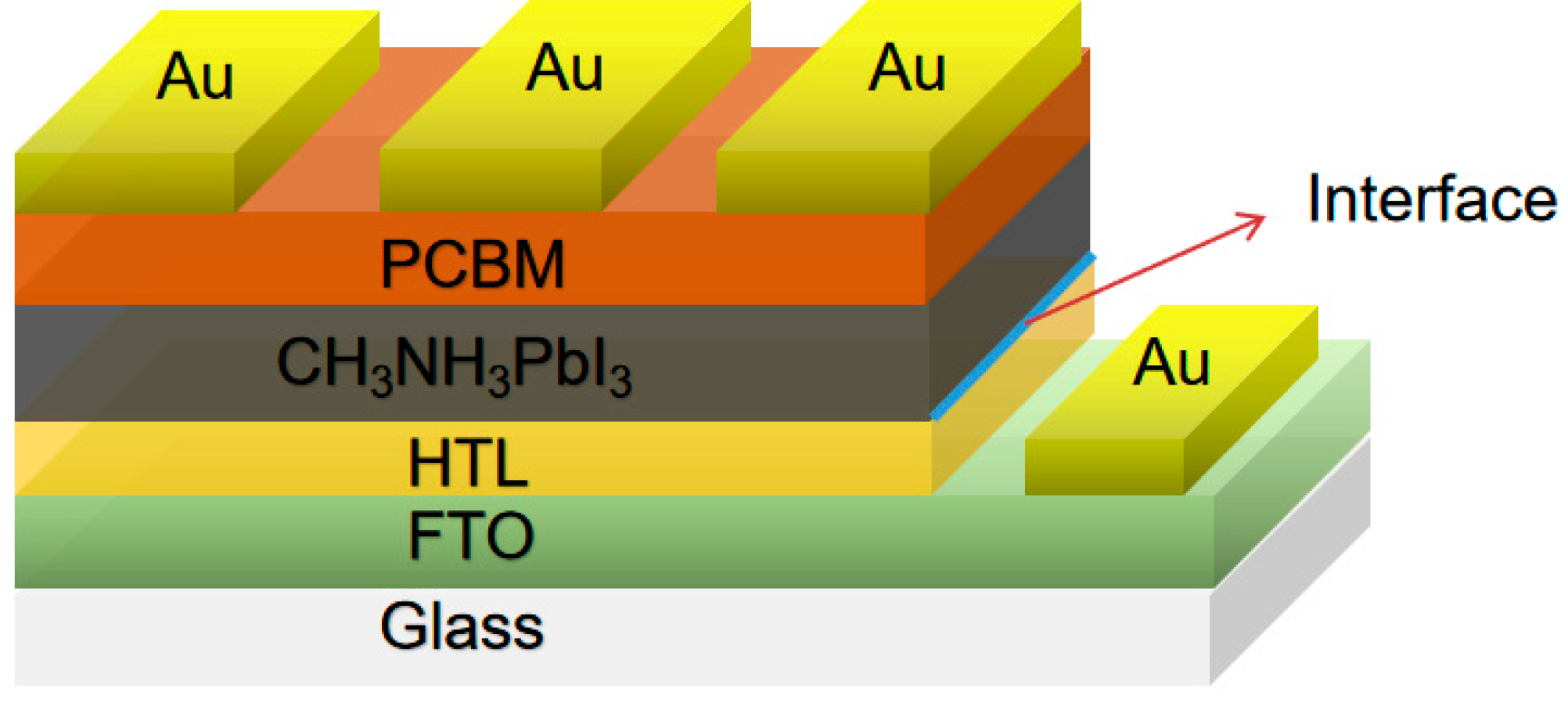
2.2. Device Fabrication

The FTO substrates were prepared by ultrasonic cleaning with the alcohol, glass water (2-propanol:deionized water:acetone = 1:1:1), and the blended solution (deionized water and detergent) for 15 min, respectively. The substrates were cleaned by ultraviolet ozone (UVO) for 90 min before spin-coating. The PEDOT:PSS solution was diluted in IPA, and then deposited on bottom substrate for 20 s at 1000 rpm. The substrate of FTO/PEDOT:PSS was placed on a hot plate for 5 min at 120 °C. Nickel oxide solution was deposited on the bottom substrate for 30 s at 4000 rpm. The FTO/NiOx substrate was annealed on a heating plate for 10 min at 150 °C and then calcined for 1 h at 350 °C in a muffle furnace with ceramic fiber (Huagang Tong Technology, Beijing, China). The PbI2 powder, completely dissolved in mixed solution of DMF and DMSO (volume ration = 1:4), spin-coated on FTO/PEDOT:PSS or FTO/NiOx substrate for 30 s at 1500 rpm. Furthermore, the MAI powder was dissolved in isopropanol solution and deposited on the PbI2 layer for 30 s at 1500 rpm. Finally, the samples were placed on a heating plate for 15 min at 150 °C.

2.3. Characterization

The microstructure of perovskite films was characterized by scanning electron microscopy (SEM) (Sigma, Zeiss, Jena, Germany). The absorption spectra of perovskite layers onto different substrates were analyzed by an ultraviolet (UV) visible absorption spectrometer (Avantes, Apeldoom, The Netherlands), and the photoluminescence spectra were examined by a LabRAW HR800 PL testing system (HORIBA Jobin Yvon, Paris, France).

2.4. Device Simulation Parameters

The device was designed with inverted structure by using sing wxAMPS. The temperature of the simulation was 300 K. The conventional parameters are listed in Table 1, as described in the results and discussion. The functional settings were as follows: defect type was neutral and the center of bandgap (Eg) was selected as defect energy level. The original defect densities of HTL and perovskite layer were 1013 cm−3 and 1014 cm−3, respectively. Gaussian energetic distribution was selected, and its characteristic energy was 0.1 eV. The original capture cross-section of function layers were 10−14 cm2. The work function of bottom and left electrode are 5.1 eV (Au) and 4.4 eV (FTO), respectively. The condition of AM1.5 illumination was applied to all simulations. A thin film (10 nm) was inserted between HTL and perovskite layer and its parameters were selected from the light absorption layer. Figure 1 shows the constitution of the PSCs. The electron transport layer we use in the simulation is [6,6]-phenyl-C61-butyric acid methyl ester (PCBM).

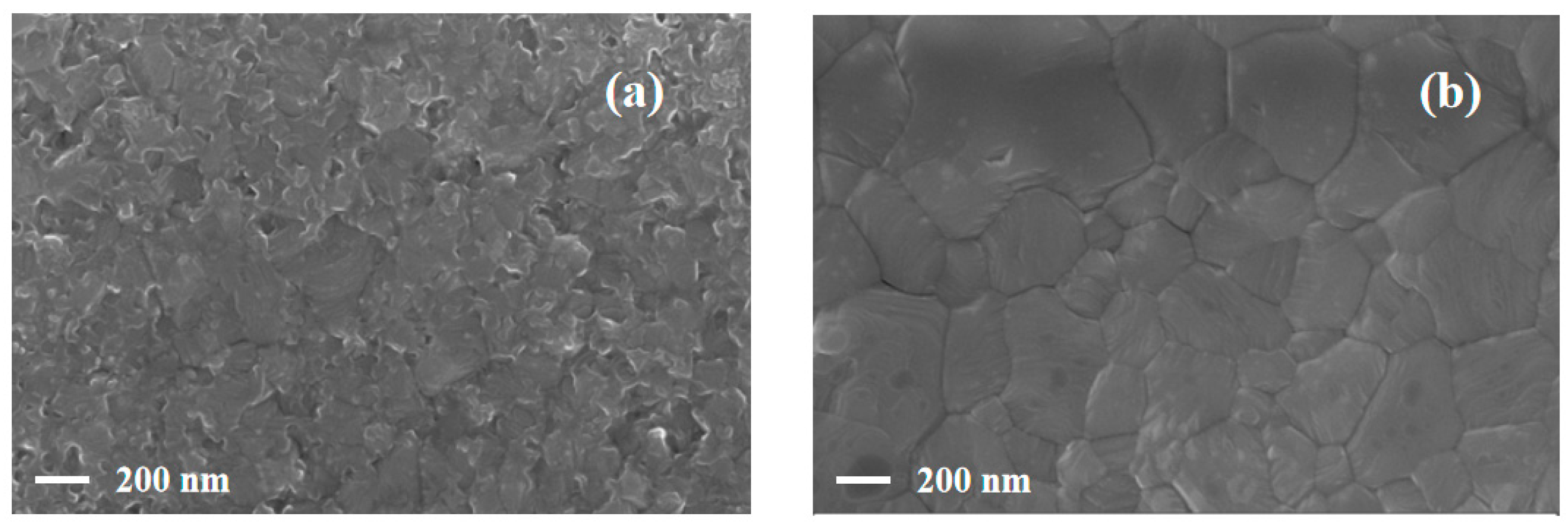
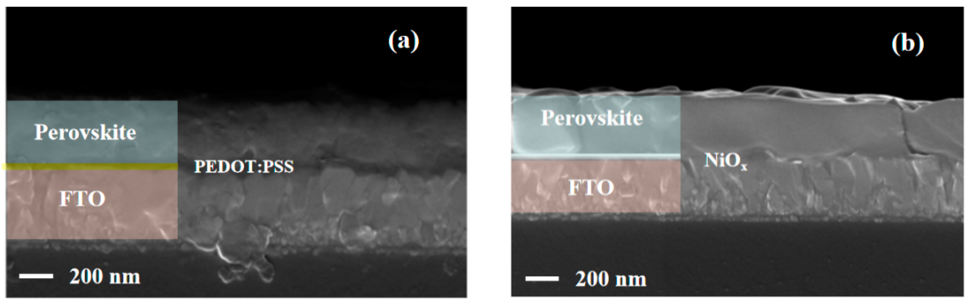
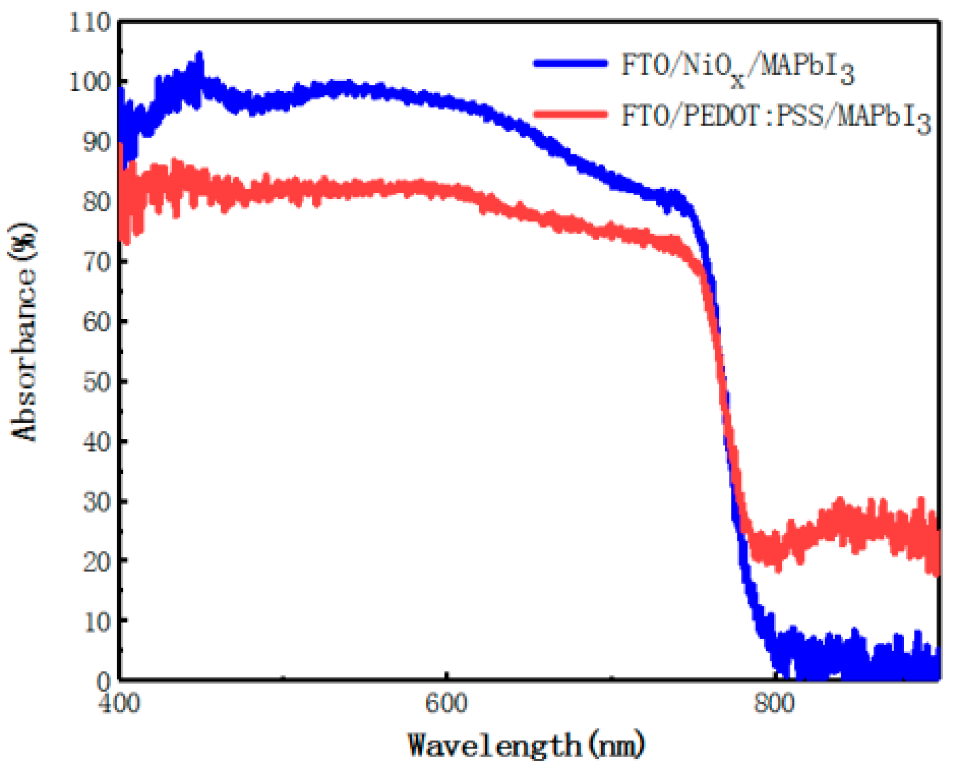
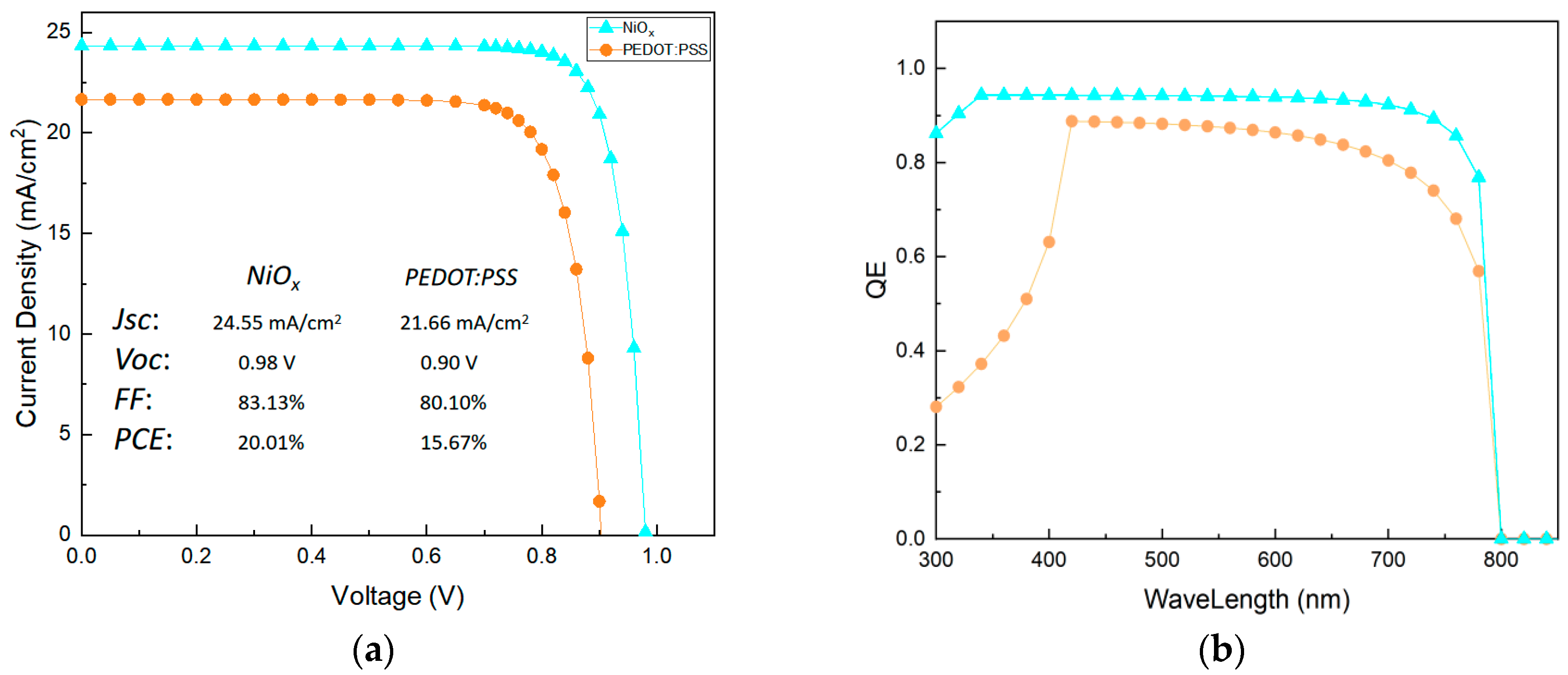
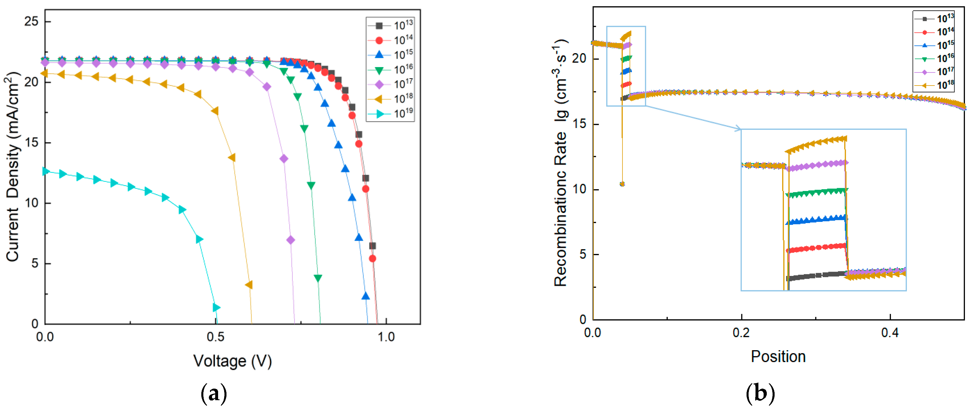
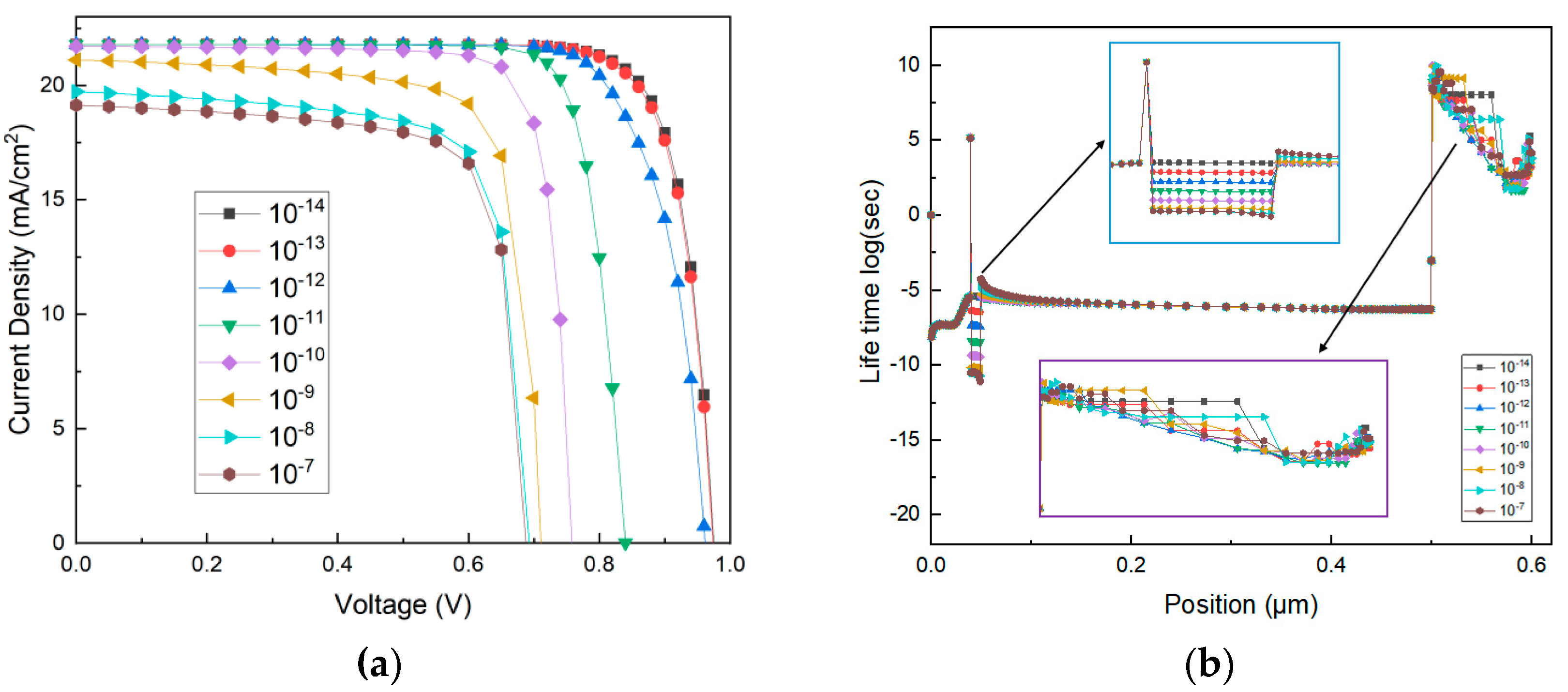
3. Results and Discussion

PEDOT:PSS and NiOx were adopted as organic and inorganic HTLs for inverted PSCs, respectively. Since the position of the valence band of NiOx is closer to that of CH3NH3PbI3 (MAPbI3), the open-circuit voltage (Voc) of the PSCs with NiOx as the HTL is higher than PEDOT:PSS [39]. The deposition of perovskite films on different organic substrates was studied in previous reports [21]. It was observed that different bottom substrates would had an influence on the growth of perovskite crystals.
The perovskite layer deposited on NiOx has a low defect density and a large grain size according to the literature report [39]. Figure 2 displays the surface morphology of perovskite layers grown on two kinds of bottom layer. The grain size of perovskite layer is smaller in Figure 2a and the accumulation of grains leads to the decrease in film flatness, which may result in the high defect density. From Figure 2b, the integral grains with large size and obvious grain boundaries are obtained. There are no pinholes on the surface and the results indicate that the NiOx bottom layer is more conducive to the deposition of the perovskite layer. The low-quality surface morphology may be ascribed to the deterioration of the interfacial layer.
To make out the influence of different HTLs on the morphology and photophysical characteristic of perovskite layers, two kinds of perovskite film with different structures (FTO/PEDOT:PSS/MAPBI3 and FTO/NiOx/MAPBI3) were prepared. From Figure 3a, the perovskite film deposited on the bottom layer has poor flatness. Past research has revealed that the hydrophilicity of PEDOT:PSS depends on the polar solvents treatment, which may impact the grain size and morphology of the perovskite [40,41]. In Figure 3b, NiOx is selected as the bottom layer of perovskite film. Compared to Figure 3a, the interface between the HTL and perovskite film is flatter. In addition, the perovskite film is compact with high quality. The main reason that PEDOT:PSS shows hygroscopicity is due to the nature of PSS (polystyrene sulfonate) [42]. Oxygen and humidity in PEDOT:PSS diffuse into the perovskite layer through the interface [43]. Perovskite structure would hydrolyze and degrade in a humid environment due to its sensitivity to moisture and oxygen, resulting in the destruction of the layered structure [26,27]. According to the report, conductive glass substrates could also be corroded by acidity, causing their components to invade the organic layer [30].
To research the impact of perovskite growth on different HTLs, the UV–vis absorption of light-absorption layers grown on two kinds of substrates (PEDOT:PSS and NiOx) are compared (Figure 4). Although there is no change in the composition of the perovskite, the enhancement of light absorption of the perovskite film deposited on NiOx layer can be seen in the wavelength ranging from 400 nm to 760 nm, which is due to improved surface morphology of perovskite film and higher optical transmittance of the NiOx layer.
The photoluminescence spectra of ITO/HTLs/perovskite structure are obtained, as shown in Figure 5. Both of the photoluminescence emission peaks are located at about 765 nm. However, the emission peaks of perovskite layers grown on organic HTL (PEDOT:PSS) was significantly increased, which was attributed to the weak hole transport capacity of PEDOT: PSS compared with that of NiOx. When the holes are transported away, the recombination of carriers is reduced, resulting in a decrease in photoluminescence intensity. Generally speaking, the lower the photoluminescence intensity, the better the device performance.
To improve the accuracy of simulation results, we set the perovskite layers deposited on the two hole transport layers with different optical absorption coefficients in the software for simulation, the parameters of which come from the absorption spectra (Figure 4). Furthermore, the above experimental data and the physical parameters of the material are combined to simulate for PSCs device by using wxAMPS. The simulation design will be introduced in the following content.
The physical parameters of different functional layers are provided in Table 1. Eg represents the band gap of different materials; Ӽe is the electron affinity; εr is the dielectric constant; μn and μp are the electron and hole mobility of the functional layer, respectively; NA and ND are the acceptor and donor impurity concentration; NC and NV are the effective density of states (DOS) of the valence band and conduction band, respectively; Value band offset is defined as the difference between the maximum value band (MVB) of the light absorbing layer and the hole transport layer. Energy diagrams of the constituting layers with different HTL materials are shown in Figure 6. These parameters are adopted from references [1,2,3,4,5,6,7,8].
The choice of hole transport layer is very important in inverted PSCs. Since light is incident from the hole transport layer side, the optical transmittance and absorption coefficient of the layer should also be considered. The introduction of these parameters will make the simulation results more accurate. As an inorganic material, NiOx has good optical transmittance. To better simulate the impact of the NiOx film on a device, the absorption coefficient of the material is calculated and is written as:
K = α λ π
where K is the extinction coefficient, α is the absorption coefficient, and λ is the wavelength. The parameters are obtained from the reports [44,45]. The absorption coefficient of the PEDOT:PSS layer is given by the Lambert–Beer law from:
A ( λ ) = lg ( 1 T ) = α ( λ )   ×   l   ×   c
where A(λ) is the absorbance; T is the light transmittance; l is the thickness of the absorbing layer and c is the concentration of the substance [46].
Figure 7a shows the J-V (current density-voltage) curves of the design PSCs with different HTLs. We can observe that the short-circuit current density (Jsc) of the PSCs with PEDOT as the HTL has a significant reduction due to the change of photophysical property of the perovskite film. The open-circuit voltage loss is also greater than that of device with NiOx as the HTL. The perovskite film deposited on NiOx layer has a high-quality morphology, so its defect density is low, resulting in a reduction in non-radiative recombination. The device series resistance increase is caused by the low hole mobility of the organic HTL and some point defects of the perovskite layer, which results in reduction of the fill factor. Therefore, the selection of the hole transport layer has an impact on the performance of the PSCs. After many simulations, it was found that when the thickness of perovskite on NiOx substrate is 390 nm, the power conversion efficiency (PCE) has the best value of 20.09%. When the thickness of perovskite on the PEDOT substrate is 620 nm, the best power conversion efficiency is 15.85%. The PCEs and J-V curves simulation results are as shown in Tables S1 and S2, Figures S1 and S2 (Supplementary Materials).
The quantum efficiency (QE) of devices with different HTLs is shown in Figure 7b. We can observe that the quantum efficiency of the device with NiOx as the HTL rises rapidly to 0.95, in the wavelength range of 300–340 nm, reaching the maximum. The difference in quantum efficiency in the front stage is caused by the difference in optical transmittance of the hole transport layer, which is reflected in the optical absorption coefficient and film thickness of the HTL. The device with NiOx as the HTL maintains a s quantum efficiency in the wavelength range of 340–750 nm, maintaining above 90%. However, the quantum efficiency of the device with PEDOT as the HTL shows significant decline within the same range, and the value is lower than that of the NiOx device. This is due to the poor morphology, and film thickness of the perovskite grown on different HTL materials. The difference is reflected in the setting of the optical absorption coefficient of the perovskite layers of different devices (refer to the absorption spectra). In addition, the decrease of quantum efficiency may be due to the lower electron and hole mobility of the PEDOT:PSS layer, which affects the collection of charge.
As mentioned before, the HTL is used as bottom side for the inverted PSCs, which impacts the growth of perovskite film. Research shows in the reference that the defect density of the interlayer between the perovskite film and the HTL has a significant influence on the performance of the device. It can be made out that the perovskite film grown on organic HTL has a structural deterioration at the interlayer from the SEM images. PEDOT:PSS showed hygroscopic due to the nature of PSS [42]. Moisture and oxygen will diffuse into the light absorption layer through the HTL, causing decomposition of perovskite and a lot of point defects at the interface [43]. On the original structure of PSCs, it is difficult to quantify the interface defect density. Therefore, an interfacial layer is inserted between HTL and perovskite film. By selecting parameters from the perovskite layer, the thickness of the film is determined to be 10 nm. However, the interface layer is of high defect density and high capture cross-section because of the destruction of the structure.
The J-V curves of devices with various defect densities of interface layer are shown in Figure 8a. It can be observed that the Voc of the device decreases unlinearly with the increase of defect density of the interface layer. The Voc of the PSCs is the same as the case of the original device, as the defect density is 1014 cm−3. As the defect density increases, the loss of Voc enhances significantly. In addition, the presence of the defect states causes a slow reduction in Jsc in the order of 1013 cm−3–1018 cm−3 and then dropping to about 13 mA/cm2 when the defect density is 1019 cm−3.
Due to the increase of the non-radiative recombination at the interface, the deep trap energy levels generated by several point defects result in the decrease of the device performance. The recombination rate of devices with different interface defect density is shown in Figure 8b. We can find that as the defect density increases, the recombination rate of the device enhances significantly at the position of 40–50 nm, which corresponds to the interlayer with a thickness of 10 nm. The point defects of deteriorated interface cause the generation of deep trap energy levels, which leads to the trap-assisted non-radiative recombination. The defect density magnitude was set in the simulation software varies from 1014 cm−3 to 1019 cm−3, which greatly affects the charge transport and recombination rate of devices. When the defect density is high, the decrease in Jsc and a significant voltage loss can be observed. Therefore, the increase in defect density generates a negative influence on device performance.
The initial capture cross-section of electrons and holes is 1014 cm2, which gives a carrier diffusion length of about 100 nm [47]. To illustrate the deterioration mechanism of the heterojunction, a thin functional layer with high capture cross-section is inserted between perovskite layer and PEDOT:PSS to research the effect of carrier lifetime on device property. The J-V curves with various capture cross sections of interface layers are shown in Figure 9a. The enhancement of capture cross section results in the voltage loss and decrease in Jsc in the range of 1014 cm to 107 cm. This indicates that the high capture cross section of the interface layer generates a negative influence on the device performance.
The degradation of device performance may be due to the enhancement of the recombination rate and reduction in carrier lifetime caused by the high capture cross-section at the interface. To account for the phenomenon, the interface layer is considered with capture cross-section varying from 10−14 cm2 to 10−7 cm2. As shown in Figure 9b, the reduction of the hole lifetime is observed in the range of 40–50 nm, corresponding to the position of the interface layer. Lifetime and recombination will affect the carrier diffusion length, which has a marked affect on the device performance. It is worth noting that the enhanced capture cross-section of the interlayer affects the carrier lifetime of electron transport layer.

4. Conclusions

In this study, the morphology and optical absorption of perovskite layers grown on different HTLs were compared. The spin-coating on different hole transport layers will affect the morphology of perovskite. Therefore, there is a certain relationship between the absorption coefficient and the morphology when the simulation is carried out in this case. The NiOx bottom layer is conducive to the growth of flat perovskite with high-quality morphology and enhancement of absorption. Then, the optical absorption parameters were introduced to the simulation software for the device design. To clarify the deteriorating interface between perovskite layer and PEDOT: PSS, a thin film with high defect density and capture cross-section was inserted, which caused the increase in recombination and reduction of carrier lifetime. The introduction of interface layer had a negative impact on device performance, manifested in the voltage loss and decrease in current density. The device design established in our work has performed well in both experiment and simulation, which supported the investigation of the impact of HTL materials and parameters of interlayer on device performance. The method combining experimental and simulated approaches, rarely used in previous studies, has great potential in studying the properties of PSCs.

Supplementary Materials

The following are available online at https://www.mdpi.com/article/10.3390/ma14092191/s1, Table S1: Device efficiencies for different perovskite film thicknesses on NiOx, Table S2: Device efficiencies for different perovskite film thicknesses on PEDOT:PSS, Figure S1: J-V curves of the device efficiencies for different perovskite film thicknesses on NiOx, Figure S2: J-V curves of the device efficiencies for different perovskite film thicknesses on PEDOT:PSS.

Author Contributions

Conceptualization, X.Z. and J.Z.; methodology, H.R.; software, J.C.; validation, X.Z., J.Z. and X.W.; formal analysis, X.W.; investigation, X.W. and Y.W.; resources, X.L.; data curation, Z.Z.; writing—original draft preparation, X.W.; writing—review and editing, C.Z.; visualization, B.R.; supervision, X.Z.; project administration, K.S. All authors have read and agreed to the published version of the manuscript.

Funding

This research was funded by the National Natural Science Foundation of China, grant number 61875186 and 61901009”, State Key Laboratory of Advanced Optical Communication Systems Networks of China (2021GZKF002) and Beijing Key Laboratory for Sensors of BISTU (No. 2019CGKF007).

Data Availability Statement

The data used to support the findings of this study are available from the corresponding author upon request.

Conflicts of Interest

The authors declare that they have no known competing financial interests or personal relationships that could have appeared to influence the work reported in this paper.

References

  1. Liu, F.; Zhu, J.; Wei, J.; Li, Y.; Lv, M.; Yang, S.; Zhang, B.; Yao, J.; Dai, S. Numerical simulation: Toward the design of high-efficiency planar perovskite solar cells. Appl. Phys. Lett. 2014, 104, 253508. [Google Scholar] [CrossRef]
  2. Wang, Y.; Xia, Z.G.; Liang, J.; Wang, X.W.; Liu, Y.M.; Liu, C.; Zhang, S.D.; Zhou, H. Towards printed perovskite solar cells with cu-prous oxide hole transporting layers: A theoretical design. Semicond. Sci. Technol. 2015, 30, 054004.1–054004.7. [Google Scholar]
  3. Wang, T.; Chen, J.; Wu, G.; Li, M. Optimal design of efficient hole transporting layer free planar perovskite solar cell. Sci. China Mater. 2016, 59, 703–709. [Google Scholar] [CrossRef] [Green Version]
  4. Yang, W.; Yao, Y.; Wu, C.-Q. Origin of the high open circuit voltage in planar heterojunction perovskite solar cells: Role of the reduced bimolecular recombination. J. Appl. Phys. 2015, 117, 095502. [Google Scholar] [CrossRef]
  5. Minemoto, T.; Murata, M. Device modeling of perovskite solar cells based on structural similarity with thin film inorganic semiconductor solar cells. J. Appl. Phys. 2014, 116, 054505. [Google Scholar] [CrossRef]
  6. Yadav, P.; Pandey, K.; Bhatt, P.; Raval, D.; Tripathi, B.; Pandey, M.K.; Kumar, M. Exploring the performance limiting parameters of perovskite solar cell through experimental analysis and device simulation. Sol. Energy 2015, 122, 773–782. [Google Scholar] [CrossRef]
  7. Casas, G.; Cappelletti, M.; Cédola, A.; Soucase, B.M.; Blancá, E.P.Y. Analysis of the power conversion efficiency of perovskite solar cells with different materials as Hole-Transport Layer by numerical simulations. Superlattices Microstruct. 2017, 107, 136–143. [Google Scholar] [CrossRef]
  8. Chouhan, A.S.; Jasti, N.P.; Avasthi, S. Effect of interface defect density on performance of perovskite solar cell: Correlation of simulation and experiment. Mater. Lett. 2018, 221, 150–153. [Google Scholar] [CrossRef] [Green Version]
  9. Li, J.; Cao, H.-L.; Jiao, W.-B.; Wang, Q.; Wei, M.; Cantone, I.; Lü, J.A. Abate. Biological impact of lead from halide perovskites re-veals the risk of introducing a safe threshold. Nat. Commun 2020, 11, 310. [Google Scholar] [CrossRef] [PubMed] [Green Version]
  10. Wang, S.; Jiao, S.; Tian, D.; Chen, H.-S.; Jiao, H.; Tu, J.; Liu, Y.; Fang, D.-N. A Novel Ultrafast Rechargeable Multi-Ions Battery. Adv. Mater. 2017, 29, 1606349. [Google Scholar] [CrossRef]
  11. Bi, D.; El-Zohry, A.M.; Hagfeldt, A.; Boschloo, G. Improved Morphology Control Using a Modified Two-Step Method for Efficient Perovskite Solar Cells. Acs. Appl. Mater. Interfaces 2014, 6, 18751–18757. [Google Scholar] [CrossRef] [PubMed]
  12. Li, W.; Fan, J.; Li, J.; Mai, Y.; Wang, L. Controllable Grain Morphology of Perovskite Absorber Film by Molecular Self-Assembly toward Efficient Solar Cell Exceeding 17%. J. Am. Chem. Soc. 2015, 137, 10399–10405. [Google Scholar] [CrossRef] [PubMed]
  13. Salim, T.; Sun, S.; Abe, Y.; Krishna, A.; Grimsdale, A.C.; Lam, Y.M. Perovskite-based solar cells: Impact of morphology and de-vice architecture on device performance. J. Mater. Chem. A 2015, 3, 8943–8969. [Google Scholar] [CrossRef]
  14. Pathak, S.; Sepe, A.; Sadhanala, A.; Deschler, F.; Haghighirad, A.; Sakai, N.; Goedel, K.C.; Stranks, S.D.; Noel, N.; Price, M.; et al. Atmospheric Influence upon Crystallization and Electronic Disorder and Its Impact on the Photophysical Properties of Organic–Inorganic Perovskite Solar Cells. Acs. Nano 2015, 9, 2311–2320. [Google Scholar] [CrossRef]
  15. Zaman, M.M.U.; Imran, M.; Saleem, A.; Komboh, A.H.; Muhammad, A.; Khan, N.; Akhter, P. Potassium doped methylammo-nium lead iodide (MAPbI3) thin films as a potential absorber for perovskite solar cells; structural, morphological, electronic and optoelectric properties. Phys. B Condens. Matter 2017, 522, 57–65. [Google Scholar] [CrossRef]
  16. Freppon, D.; Men, L.; Burkhow, S.J.; Petrich, J.W.; Vela, J.; Smith, E.A. Photophysical properties of wavelength-tunable me-thylammonium lead halide perovskite nanocrystals. J. Mater. Chem. C 2017, 5, 118–126. [Google Scholar] [CrossRef] [Green Version]
  17. Kim, M.K.; Lee, H.S.; Pae, S.R.; Kim, S.R.; Lee, D.J.; Gereige, J.Y.; Park, I.; Shin, S. Effects of temperature and coating speed on the morphology of solution-sheared halide perovskite thin-film. J. Mater. Chem. A 2018, 48, 24911–24919. [Google Scholar] [CrossRef]
  18. Sara, B.N.; Luo, B.B.; Abdelmageed, G.; Pu, Y.C.; Zhang, C.; Jin, Z. Photophysical properties and improved stability of organ-ic-inorganic perovskite by surface passivation. J. Phys. Chem. C 2018, 122, 5799–15818. [Google Scholar]
  19. Li, J.; Huang, J.; Zhao, A.; Li, Y.; Wei, M. An inorganic stable Sn-based perovskite film with regulated nucleation for solar cell application. J. Mater. Chem. C 2020, 8, 8840–8845. [Google Scholar] [CrossRef]
  20. Meng, L.; You, J.; Guo, T.-F.; Yang, Y. Recent Advances in the Inverted Planar Structure of Perovskite Solar Cells. Acc. Chem. Res. 2016, 49, 155–165. [Google Scholar] [CrossRef] [PubMed]
  21. Lin, Q.; Armin, A.; Nagiri, R.C.R.; Burn, P.L.; Meredith, P. Electro-optics of perovskite solar cells. Nat. Photon. 2015, 9, 106–112. [Google Scholar] [CrossRef]
  22. You, J.; Yang, Y.; Hong, Z.; Song, T.-B.; Meng, L.; Liu, Y.; Jiang, C.; Zhou, H.; Chang, W.-H.; Li, G. Moisture assisted perovskite film growth for high performance solar cells. Appl. Phys. Lett. 2014, 105, 183902. [Google Scholar] [CrossRef] [Green Version]
  23. Heo, J.H.; Han, H.J.; Kim, D.; Ahn, T.K.; Im, S.H. Hysteresis-less inverted CH3NH3PbI3 planar perovskite hybrid solar cells with 18.1% power conversion efficiency. Energy Environ. Sci. 2015, 8, 1602–1608. [Google Scholar] [CrossRef]
  24. Jeng, J.-Y.; Chiang, Y.-F.; Lee, M.-H.; Peng, S.-R.; Guo, T.-F.; Chen, P.; Wen, T.-C. CH3NH3PbI3Perovskite/Fullerene Planar-Heterojunction Hybrid Solar Cells. Adv. Mater. 2013, 25, 3727–3732. [Google Scholar] [CrossRef] [PubMed]
  25. Sun, S.Y.; Salim, T.; Mathews, N.; Duchamp, M.; Boothroyd, C.; Xing, G.; Sum, T.C.; Lam, Y.M. The origin of high efficiency in lowtemperature solution-processable bilayer organometal halide hybridsolar cells. Energy Environ. Sci. 2014, 7, 399–407. [Google Scholar] [CrossRef] [Green Version]
  26. Jørgensen, M.; Norrman, K.; Krebs, F.C. Stability/degradation of polymer solar cells. Sol. Energy Mater. Sol. Cells 2008, 92, 686–714. [Google Scholar] [CrossRef]
  27. Kawano, K.; Pacios, R.; Poplavskyy, D.; Nelson, J.; Bradley, D.D.; Durrant, J.R. Degradation of organic solar cells due to air exposure. Sol. Energy Mater. Sol. Cells 2006, 90, 3520–3530. [Google Scholar] [CrossRef]
  28. Pacios, R.; Chatten, A.; Kawano, K.; Durrant, J.R.; Nelson, J.; Bradleyc, D.D.C. Effects of Photo-oxidation on the Performance of Poly[2-methoxy-5-(3′,7′-dimethyloctyloxy)-1,4-phenylenevinylene]:[6,6]-Phenyl C61-Butyric Acid Methyl Ester Solar Cells. Adv. Funct. Mater. 2010, 16, 2117–2126. [Google Scholar] [CrossRef]
  29. Li, J.; Hu, P.; Chen, Y.; Li, Y.; Wei, M. Enhanced Performance of Sn-Based Perovskite Solar Cells by Two-Dimensional Perovskite Doping. Acs. Sustain. Chem. Eng. 2020, 8, 8624–8628. [Google Scholar] [CrossRef]
  30. White, M.S.; Olson, D.C.; Shaheen, S.E.; Kopidakis, N.; Ginley, D.S. Inverted bulk-heterojunction organic photovoltaic device using a solution-derived ZnO underlayer. Appl. Phys. Lett. 2006, 89, 143517. [Google Scholar] [CrossRef]
  31. Takahashi, K.; Suzaka, S.; Sigeyama, Y.; Yamaguchi, T.; Yamaguchi, T.; Nakamura, J. Efficiency Increase by Insertion of Electro-deposited CuSCN Layer into ITO/Organic Solid Interface in Bulk Hetero-junction Solar Cells Consisting of Polythiophene and Fullerene. Chem. Lett. 2007, 36, 762–763. [Google Scholar] [CrossRef]
  32. Irwin, M.D.; Buchholz, D.B.; Hains, A.W.; Chang, R.P.H.; Markset, T.J. p-Type semiconducting nickel oxide as an efficien-cy-enhancing anode interfacial layer in polymer bulk-heterojunction solar cells. Proc. Natl. Acad. Sci. USA 2008, 105, 2783–2787. [Google Scholar] [CrossRef] [Green Version]
  33. Zuo, C.; Ding, L. Solution-Processed Cu2O and CuO as Hole Transport Materials for Efficient Perovskite Solar Cells. Small 2015, 11, 5528–5532. [Google Scholar] [CrossRef]
  34. Wang, S.; Jiao, S.; Wang, J.; Chen, H.-S.; Tian, D.; Lei, H.; Fang, D.-N. High-performance aluminum-ion battery with CuS@ C mi-crosphere composite cathode. Acs. Nano 2017, 11, 469–477. [Google Scholar] [CrossRef] [PubMed]
  35. Sajid, S.; Elseman, A.M.; Huang, H.; Ji, J.; Dou, S.; Jiang, H.; Liu, X.; Wei, D.; Cui, P.; Li, M. Breakthroughs in NiOx-HTMs towards Stable, Low-Cost and Efficient Perovskite Solar Cells. Nano Energy 2018, 51, 408–424. [Google Scholar] [CrossRef]
  36. Chen, P.-C.; Yang, S.-H. Potassium-Doped Nickel Oxide as the Hole Transport Layer for Efficient and Stable Inverted Perovskite Solar Cells. Acs. Appl. Energy Mater. 2019, 2, 6705–6713. [Google Scholar] [CrossRef]
  37. Wang, S.; Zhu, Y.; Wang, C.Y.; Ma, R.X. NH4F as an interfacial modifier for high performance NiOx-based inverted perovskite solar cells. Org. Electron. 2020, 78, 105627. [Google Scholar] [CrossRef]
  38. Lian, X.; Chen, J.; Shan, S.; Wu, G.; Chen, H. Polymer Modification on NiOx Hole Transport Layer Boosts Open-Circuit Voltage to 1.19 V for Perovskite Solar Cells. Acs. Appl. Mater. Interfaces 2020, 12, 46340–46347. [Google Scholar] [CrossRef]
  39. You, J.; Meng, L.; Song, T.-B.; Guo, T.-F.; Yang, Y.; Chang, W.-H.; Hong, Z.; Chen, H.; Zhou, H.; Chen, Q.; et al. Improved air stability of perovskite solar cells via solution-processed metal oxide transport layers. Nat. Nanotechnol. 2016, 11, 75–81. [Google Scholar] [CrossRef] [PubMed]
  40. Wu, P.-T.; Tsai, M.-C.; Guo, T.-F.; Fu, Y.-S. The impact at polar solvent treatment on p-contact layers (PEDOT:PSS or NiOx) of hybrid perovskite solar cells. Org. Electron. 2019, 73, 273–278. [Google Scholar] [CrossRef]
  41. Bi, C.; Wang, Q.; Shao, Y.; Yuan, Y.; Xiao, Z.; Huang, J. Non-wetting surface-driven high-aspect-ratio crystalline grain growth for efficient hybrid perovskite solar cells. Nat. Commun. 2015, 6, 7747. [Google Scholar] [CrossRef] [PubMed]
  42. De Jong, M.M.; Van Ijzendoorn, L.L.; De Voigt, M.M. Stability of the interface between indium-tin-oxide and poly(3,4-ethylenedioxythiophene)/poly(styrenesulfonate) in polymer light-emitting diodes. Appl. Phys. Lett. 2000, 77, 2255–2257. [Google Scholar] [CrossRef]
  43. Voroshazi, E.; Verreet, B.; Buri, A.; Müllera, R.; Nuzzod, D.D.; Heremans, P. Influence of cathode oxidation via the hole extrac-tion layer in polymer:fullerene solar cells. Org. Electron. 2011, 12, 736–744. [Google Scholar] [CrossRef]
  44. Sriram, S.; Thayumanavan, A. Structural, Optical and Electrical Properties of NiO Thin Films Prepared by Low Cost Spray Pyrolysis Technique. Int. J. Mater. Sci. Eng. 2014, 1, 118–121. [Google Scholar] [CrossRef]
  45. Sato, K.; Kim, S.; Komuro, S.; Zhao, X. Characteristics of Cu-doped amorphous NiO thin films formed by RF magnetron sputtering. Jpn. J. Appl. Phys. 2016, 55, 06GJ10. [Google Scholar] [CrossRef]
  46. Talukdara, H.; Sarkar, S.; Kundu, S. Electrical Investigation on Thin Films of Poly(3,4-Ethylenedioxythiophene): Poly (Sty-renesulfonate) in Presence of Cationic Polyelectrolyte. Aip. Conf. Proc. 2019, 2115, 030286. [Google Scholar]
  47. Ning, W.; Wang, F.; Wu, B.; Lu, J.; Yan, Z.; Liu, X.; Tao, Y.; Liu, J.; Huang, W.; Fahlman, M. Long Electron-Hole Diffusion Length in High-Quality Lead-Free Double Perovskite Films. Adv. Mater. 2018, 30, 1706246. [Google Scholar] [CrossRef]
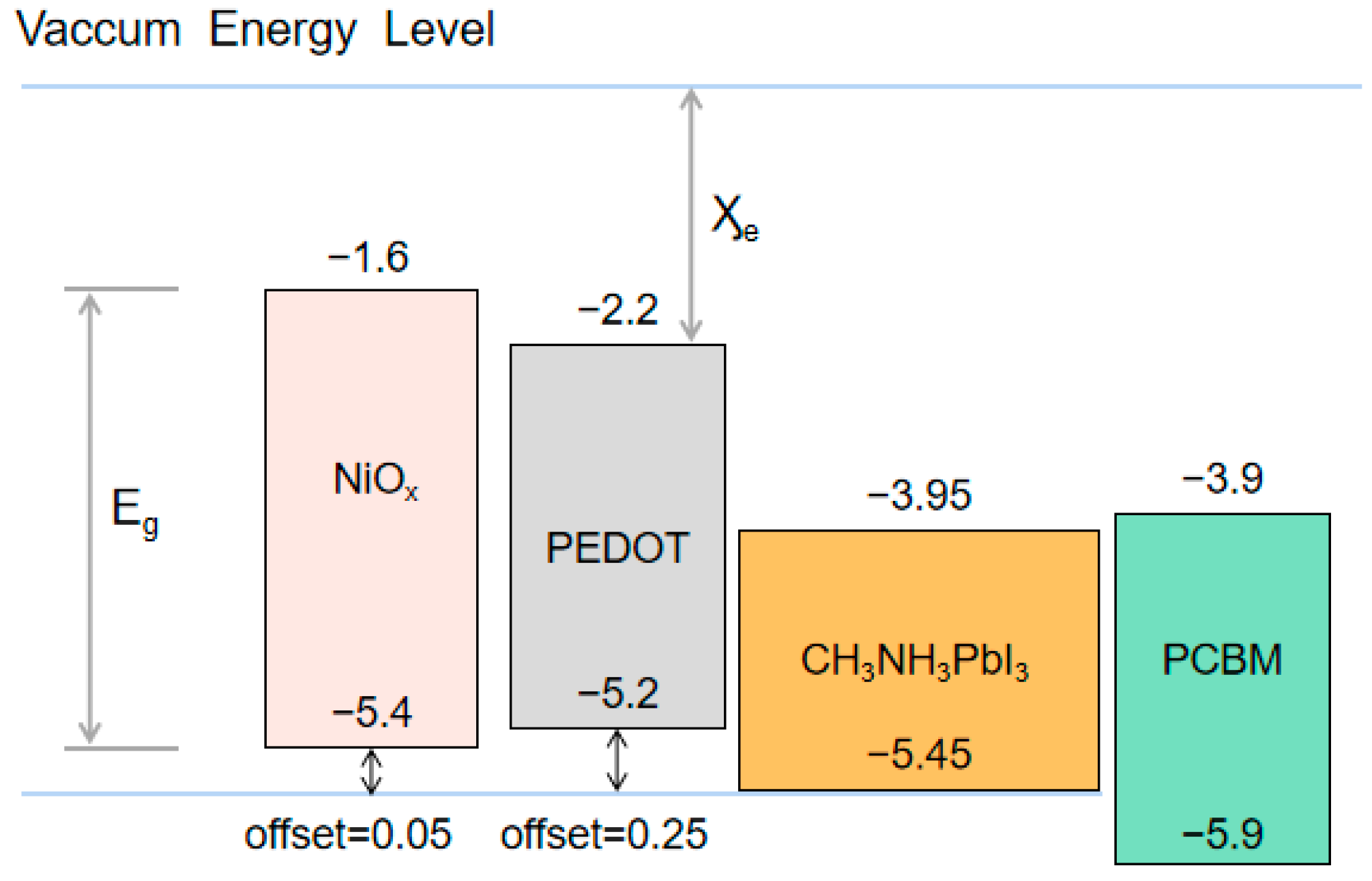
Figure 1. The device structure for simulation design.
Materials 14 02191 g001
Figure 2. Scanning electron microscope (SEM) top-view of perovskite layers: (a) the sample of fluorine-doped SnO2/polyethylene dioxythiophene:poly (styrene sulfonate) (FTO/PEDOT:PSS/MAPbI3); (b) the sample of FTO/NiOx/MAPbI3.
Materials 14 02191 g002
Figure 3. Cross-sectional SEM images: (a) the sample of FTO/PEDOT:PSS/MAPbI3; (b) the sample of FTO/NiOx/MAPbI3.
Materials 14 02191 g003
Figure 4. Ultraviolet–visible (UV–Vis) absorption spectra of perovskite films on different hole transport layers (HTL).
Materials 14 02191 g004
Figure 5. Photoluminescence spectra of perovskite light-absorption layer films deposited on different HTLs.
Materials 14 02191 g005
Figure 6. Energy diagrams of the constituting layers with different HTL materials.
Materials 14 02191 g006
Figure 7. Simulation results of the proposed PSC with different HTL (a) J-V curves (b) quantum efficiency (QE) curves.
Materials 14 02191 g007
Figure 8. Simulation results of the proposed PSC with different defect density (cm−3) of the interface between PEDOT:PSS and CH3NH3PbI3 (a) J-V curves (b) recombination rate.
Materials 14 02191 g008
Figure 9. Simulation of the proposed PSC with capture cross-section (cm2) of interface between PEDOT:PSS and CH3NH3PbI3 (a) J-V curves (b) hole lifetime.
Materials 14 02191 g009
Table 1. Basic parameters for simulation of perovskite solar cells (PSCs) in this study [1,2,3,4,5,6,7,8].
Basic ParametersNiOxPEDOT:PSSInterface LayerCH3NH3PbI3PCBM
Eg (eV)3.831.51.52
Ӽe (eV)1.62.23.953.953.9
εr117.530303.9
Thickness (nm)304010500/450100
μn (cm2V−1s−1)2.8014140.2
μp (cm2V−1s−1)2.80.00114140
NA(cm3)1.5 × 10181 × 10186 × 10146 × 10140
ND(cm−3)00002.93 × 1017
NC(cm−3)1 × 10181 × 10162.5 × 10202.5 × 10202.5 × 1021
NV(cm−3)1 × 10181 × 10192.5 × 10202.5 × 10202.5 × 1021
Value band offset (eV)0.050.25---
Publisher’s Note: MDPI stays neutral with regard to jurisdictional claims in published maps and institutional affiliations.

