
Parasitic Current Induced by Gate Overlap in Thin-Film Transistors


Abstract
:1. Introduction
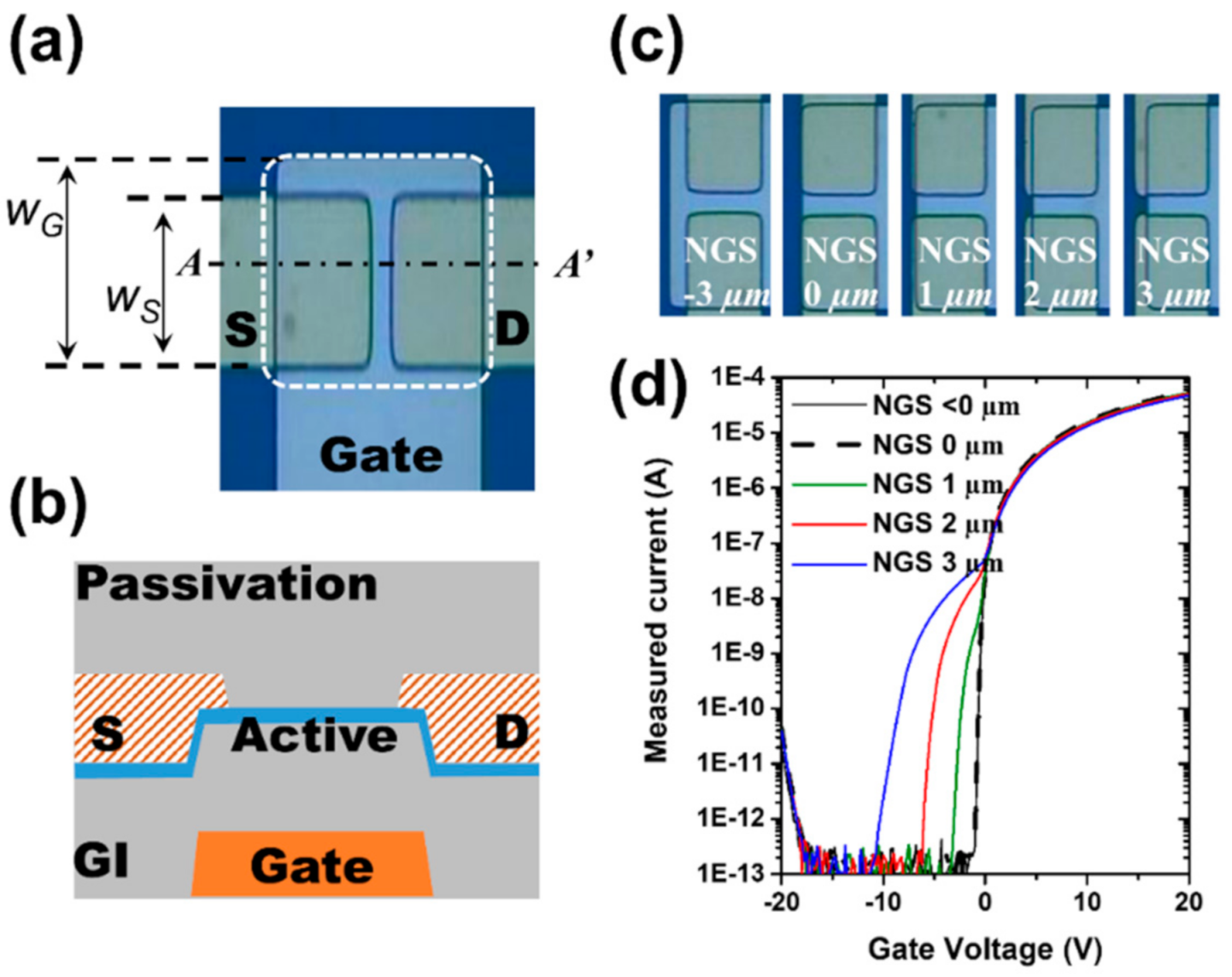
2. Devices and Experiment
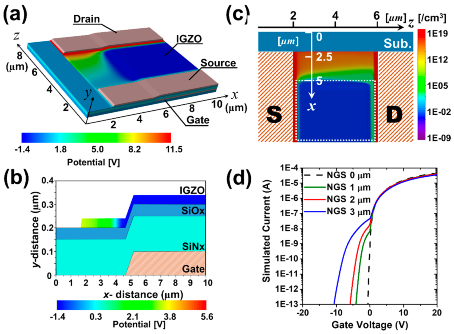
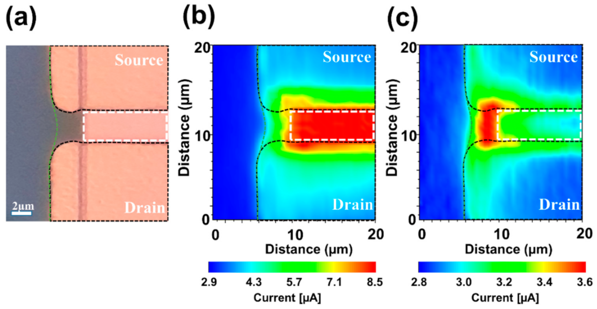
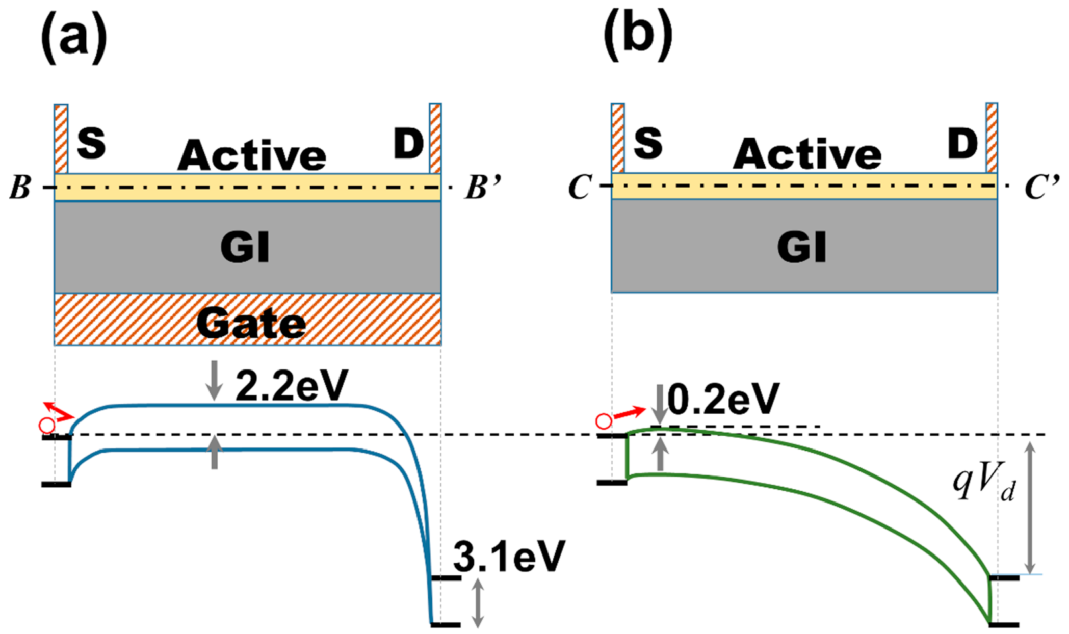
3. Results and Discussion
4. Conclusions
Author Contributions
Funding
Institutional Review Board Statement
Informed Consent Statement
Data Availability Statement
Conflicts of Interest
References
- Nomura, K.; Ohta, H.; Ueda, K.; Kamiya, T.; Hirano, M.; Hosono, H. Thin-film transistor fabricated in single-crystalline transparent oxide semiconductor. Science 2003, 300, 1269–1272. [Google Scholar] [CrossRef]
- Takahashi, T.; Fujii, M.N.; Miyanaga, R.; Miyanaga, M.; Ishikawa, Y.; Uraoka, Y. Unique degradation under AC stress in high-mobility amorphous In–W–Zn–O thin-film transistors. Appl. Phys. Express 2020, 13, 054003. [Google Scholar] [CrossRef]
- Lee, H.; Abe, K. A Study on the Effect of Pulse Rising and Falling Time on Amorphous Oxide Semiconductor Transistors in Driver Circuits. IEEE Electron Device Lett. 2020, 41, 896–899. [Google Scholar] [CrossRef]
- Takahashi, T.; Miyanaga, R.; Fujii, M.N.; Tanaka, J.; Takechi, K.; Tanabe, H.; Bermundo, J.P.; Ishikawa, Y.; Uraoka, Y. Hot carrier effects in InGaZnO thin-film transistor. Appl. Phys. Express 2019, 12, 094007. [Google Scholar] [CrossRef]
- Noh, H.Y.; Kim, J.; Kim, J.-S.; Lee, M.-J.; Lee, H.-J. Role of Hydrogen in Active Layer of Oxide-Semiconductor-Based Thin Film Transistors. Crystals 2019, 9, 75. [Google Scholar] [CrossRef] [Green Version]
- Hong, S.Y.; Kim, H.J.; Kim, D.H.; Jeong, H.Y.; Song, S.H.; Cho, I.T.; Noh, J.; Yun, P.S.; Lee, S.W.; Park, K.S.; et al. Study on the Lateral Carrier Diffusion and Source-Drain Series Resistance in Self-Aligned Top-Gate Coplanar InGaZnO Thin-Film Transistors. Sci. Rep. 2019, 9, 6588. [Google Scholar] [CrossRef] [PubMed]
- Yang, C.; Chang, T.; Liao, P.; Chen, L.; Chen, B.; Chou, W.; Chen, G.; Lin, S.; Yeh, C.; Tsai, C.; et al. Drain-Induced-Barrier-Lowing-Like Effect Induced by Oxygen-Vacancy in Scaling-Down via-Contact Type Amorphous InGaZnO Thin-Film Transistors. IEEE J. Electron Devices Soc. 2018, 6, 685–690. [Google Scholar] [CrossRef]
- Myny, K. The development of flexible integrated circuits based on thin-film transistors. Nat. Electron. 2018, 1, 30–39. [Google Scholar] [CrossRef]
- Chen, H.T.; Cao, Y.; Zhang, J.L.; Zhou, C.W. Large-scale complementary macroelectronics using hybrid integration of carbon nanotubes and IGZO thin-film transistors. Nat. Commun. 2014, 5, 4097. [Google Scholar] [CrossRef]
- Ide, K.; Nomura, K.; Hosono, H.; Kamiya, T. Electronic Defects in Amorphous Oxide Semiconductors: A Review. Phys. Status Solidi 2019, 216, 1800372. [Google Scholar] [CrossRef]
- Fortunato, E.; Barquinha, P.; Martins, R. Oxide semiconductor thin-film transistors: A review of recent advances. Adv. Mater. 2012, 24, 2945–2986. [Google Scholar] [CrossRef] [PubMed]
- Lee, H.-J.; Cho, S.H.; Abe, K.; Lee, M.-J.; Jung, M. Impact of transient currents caused by alternating drain stress in oxide semiconductors. Sci. Rep. 2017, 7, 9782–9790. [Google Scholar] [CrossRef] [Green Version]
- Lee, S.; Li, X.; Mativenga, M.; Jang, J. Bulk-Accumulation Oxide Thin-Film Transistor Circuits with Zero Gate-to-Drain Overlap Capacitance for High Speed. IEEE Electron Device Lett. 2015, 36, 1329–1331. [Google Scholar] [CrossRef]
- Jeong, J.; Hong, Y. Gate Overlap Optimization and Performance Variation for Thin-Film Transistors with Source/Drain Edge Waviness. Jpn. J. Appl. Phys. 2010, 49, 036501. [Google Scholar] [CrossRef]
- Lee, H.-J.; Abe, K.; Noh, H.Y.; Kim, J.-S.; Lee, H.; Lee, M.-J. Analysis of the hump phenomenon and needle defect states formed by driving stress in the oxide semiconductor. Sci. Rep. 2019, 9, 11977. [Google Scholar] [CrossRef]
- Mativenga, M.; Haque, F.; Um, J.G.; Siddik, A.B. Impact of Source-to-Gate and Drain-to-Gate Overlap Lengths on Performance of Inverted Staggered a-IGZO TFTs with an Etch Stopper. IEEE Trans. Electron Devices 2020, 67, 3152–3156. [Google Scholar] [CrossRef]
- Valletta, A.; Gaucci, P.; Mariucci, L.; Fortunato, G.; Templier, F. “Hump” characteristics and edge effects in polysilicon thin film transistors. J. Appl. Phys. 2008, 104, 124511. [Google Scholar] [CrossRef]
- Huang, C.F.; Peng, C.Y.; Yang, Y.J.; Sun, H.C.; Chang, H.C.; Kuo, P.S.; Chang, H.L.; Liu, C.Z.; Liu, C.W. Stress-Induced Hump Effects of p-Channel Polycrystalline Silicon Thin-Film Transistors. IEEE Electron Device Lett. 2008, 29, 1332–1335. [Google Scholar] [CrossRef]
- Mativenga, M.; Seok, M.; Jang, J. Gate bias-stress induced hump-effect in transfer characteristics of amorphous-indium-galium-zinc-oxide thin-fim transistors with various channel widths. Appl. Phys. Lett. 2011, 99, 122107. [Google Scholar] [CrossRef]
- Choi, S.-H.; Han, M.-K. Effect of channel widths on negative shift of threshold voltage, including stress-induced hump phenomenon in InGaZnO thin-film transistors under high-gate and drain bias stress. Appl. Phys. Lett. 2012, 100, 043503–043505. [Google Scholar] [CrossRef] [Green Version]
- Tsai, M.-Y.; Chang, T.-C.; Chu, A.-K.; Hsieh, T.-Y.; Chen, T.-C.; Lin, K.-Y.; Tsai, W.-W.; Chiang, W.-J.; Yan, J.-Y. High temperature-induced abnormal suppression of sub-threshold swing and on-current degradations under hot-carrier stress in a-InGaZnO thin film transistors. Appl. Phys. Lett. 2013, 103, 012101. [Google Scholar] [CrossRef]
- Jeong, C.-Y.; Lee, D.; Song, S.-H.; Kim, J.I.; Lee, J.-H.; Kwon, H.-I. A study on the degradation mechanism of InGaZnO thin-film transistors under simultaneous gate and drain bias stresses based on the electronic trap characterization. Semicond. Sci. Technol. 2014, 29, 045023. [Google Scholar] [CrossRef]
- Hwarim, I.; Hyunsoo, S.; Jaewook, J.; Yewon, H.; Yongtaek, H. Effects of defect creation on bidirectional behavior with hump characteristics of InGaZnO TFTs under bias and thermal stress. Jpn. J. Appl. Phys. 2015, 54, 03CB03. [Google Scholar]
- Lee, H.-J.; Abe, K.; Kim, J.S.; Lee, M.-J. Electron-blocking by the potential barrier originated from the asymmetrical local density of state in the oxide semiconductor. Sci. Rep. 2017, 7, 17963–17970. [Google Scholar] [CrossRef] [PubMed] [Green Version]
- Lee, H.-J.; Abe, K.; Cho, S.H.; Kim, J.; Bang, S.; Lee, M. Drain-Induced Barrier Lowering in Oxide Semiconductor Thin-Film Transistors with Asymmetrical Local Density of States. IEEE J. Electron Devices Soc. 2018, 6, 830–834. [Google Scholar] [CrossRef]
- Furuta, M.; Kamada, Y.; Kimura, M.; Hiramatsu, T.; Matsuda, T.; Furuta, H.; Li, C.; Fujita, S.; Hirao, T. Analysis of Hump Characteristics in Thin-Film Transistors with ZnO Channels Deposited by Sputtering at Various Oxygen Partial Pressures. IEEE Electron Device Lett. 2010, 31, 1257–1259. [Google Scholar] [CrossRef] [Green Version]
- Lee, M.-J.; Ahn, J.-H.; Sung, J.H.; Heo, H.; Jeon, S.G.; Lee, W.; Song, J.Y.; Hong, K.-H.; Choi, B.; Lee, S.-H.; et al. Thermoelectric materials by using two-dimensional materials with negative correlation between electrical and thermal conductivity. Nat. Commun. 2016, 7, 12011. [Google Scholar] [CrossRef] [Green Version]
- Sze, S.M.; Li, Y.; Ng, K.K. Physics of Semiconductor Devices, 3rd ed.; John Wiley & Sons: Hoboken, NJ, USA, 2006. [Google Scholar]


Publisher’s Note: MDPI stays neutral with regard to jurisdictional claims in published maps and institutional affiliations. |
© 2021 by the authors. Licensee MDPI, Basel, Switzerland. This article is an open access article distributed under the terms and conditions of the Creative Commons Attribution (CC BY) license (https://creativecommons.org/licenses/by/4.0/).
Share and Cite
Lee, H.-J.; Abe, K.; Kim, J.-S.; Yun, W.S.; Lee, M.-J. Parasitic Current Induced by Gate Overlap in Thin-Film Transistors. Materials 2021, 14, 2299. https://doi.org/10.3390/ma14092299
Lee H-J, Abe K, Kim J-S, Yun WS, Lee M-J. Parasitic Current Induced by Gate Overlap in Thin-Film Transistors. Materials. 2021; 14(9):2299. https://doi.org/10.3390/ma14092299
Chicago/Turabian StyleLee, Hyeon-Jun, Katsumi Abe, June-Seo Kim, Won Seok Yun, and Myoung-Jae Lee. 2021. "Parasitic Current Induced by Gate Overlap in Thin-Film Transistors" Materials 14, no. 9: 2299. https://doi.org/10.3390/ma14092299