Article

Performance Comparison of Lattice-Matched AlInN/GaN/AlGaN/GaN Double-Channel Metal–Oxide–Semiconductor High-Electron Mobility Transistors with Planar Channel and Multiple-Mesa-Fin-Channel Array

1
Department of Photonics, National Cheng Kung University, Tainan 701, Taiwan
2
Department of Electrical Engineering, National Central University, Zhongli 32001, Taiwan
3
Department of Electrical Engineering, Yuan Ze University, Taoyuan 320, Taiwan
*
Author to whom correspondence should be addressed.
Materials 2022, 15(1), 42; https://doi.org/10.3390/ma15010042
Submission received: 8 October 2021 / Revised: 18 December 2021 / Accepted: 19 December 2021 / Published: 22 December 2021

Abstract

:
In this work, Al0.83In0.17N/GaN/Al0.18Ga0.82N/GaN epitaxial layers used for the fabrication of double-channel metal–oxide–semiconductor high-electron mobility transistors (MOSHEMTs) were grown on silicon substrates using a metalorganic chemical vapor deposition system (MOCVD). A sheet electron density of 1.11 × 1013 cm−2 and an electron mobility of 1770 cm2/V-s were obtained. Using a vapor cooling condensation system to deposit high insulating 30-nm-thick Ga2O3 film as a gate oxide layer, double-hump transconductance behaviors with associated double-hump maximum extrinsic transconductances (gmmax) of 89.8 and 100.1 mS/mm were obtained in the double-channel planar MOSHEMTs. However, the double-channel devices with multiple-mesa-fin-channel array with a gmmax of 148.9 mS/mm exhibited single-hump transconductance behaviors owing to the better gate control capability. Moreover, the extrinsic unit gain cutoff frequency and maximum oscillation frequency of the devices with planar channel and multiple-mesa-fin-channel array were 5.7 GHz and 10.5 GHz, and 6.5 GHz and 12.6 GHz, respectively. Hooge’s coefficients of 7.50 × 10⁻⁵ and 6.25 × 10⁻⁶ were obtained for the devices with planar channel and multiple-mesa-fin-channel array operating at a frequency of 10 Hz, drain–source voltage of 1 V, and gate–source voltage of 5 V, respectively.

1. Introduction

In recent decades, silicon (Si)-based electronic devices have become dominant power devices used in various systems. To enhance their capability of operating at a higher voltage, higher current, higher temperature, higher frequency, and with better energy efficiency, gallium nitride (GaN)-based electronic devices have played the mainstream role of power semiconductor devices, which have recently benefited from their superior electrical and physical properties [1,2,3]. Despite the success of depletion-mode and enhancement-mode GaN-based single-channel metal–oxide–semiconductor high-electron mobility transistors (MOSHEMTs), active development of high-performance compelling devices is still needed. In general, the enhancement of both electron mobility (μn) and sheet electron density (nch) has been widely explored with the aim of improving the performances of GaN-based MOSHEMTs. However, it is technically difficult to grow an AlGaN layer with high Al content to achieve high μn and nch simultaneously. Recently, to simultaneously obtain both the enhanced μn and nch, multiple-channel structures were explored [4,5,6,7]. Furthermore, superior performances of higher current drive, low resistance, low-frequency noise, and improved linearity were demonstrated in multiple-channel MOSHEMTs [8,9,10]. Nevertheless, since lattice-matched heterostructured structures could reduce the failure caused by the inverse piezoelectric effect [11], lattice-matched barrier layers in multiple-channel structures remain a promising candidate for enhancing performance [12,13,14]. In this work, double-channel epitaxial layers of lattice-matched Al0.83In0.17N/GaN/Al0.18Ga0.82N/GaN were grown on Si substrates using a metalorganic chemical deposition (MOCVD, AIXTRON Group, Herzogenrath, Germany) system. Although several gate oxide layers were used in GaN-based MOSHEMTs [15,16,17,18,19,20], gallium oxide (Ga2O3)-based materials have become promising gate oxide layers due to their superior properties of high breakdown voltage, high radiation resistance, high thermal and chemical stability, high Baliga’s figure-of-merit, and better interface properties between Ga2O3 film and GaN-based semiconductors [21,22,23]. Furthermore, because high-quality and high-insulating amorphous Ga2O3 films could be deposited using a vapor cooling condensation system [24,25] and were successfully used in GaN-based MOSHEMTs previously [25,26], the system was used to deposit a 30-nm-thick Ga2O3 film as a gate oxide layer in this work. In addition, to improve interface properties, surface preparation was employed previously [27]. In this study, before depositing the Ga2O3 gate oxide layer, an (NH4)2Sx chemical solution was used to treat the sample surface to completely remove the undesired native oxide residing on the surface of the GaN-based semiconductors [28]. Recently, lattice-matched double-channel AlInN/GaN/AlGaN/GaN MOSHEMTs with multiple-mesa-fin-channel array were reported [29]. Although the compared performances of signal-channel MOSHEMTs with planar channel and multiple-mesa-fin-channel array were reported previously [30,31], a comparison of the performances of the multiple-channel MOSHEMTs with planar channel and multiple-mesa-fin-channel array has not yet been carried out. In this work, to compare the performances of the planar channel structure with the multiple-mesa-fin-channel array of double-channel MOSHEMTs, lattice-matched double-channel Al0.83In0.17N/GaN/Al0.18Ga0.82N/GaN MOSHEMTs with planar channel were fabricated and studied.

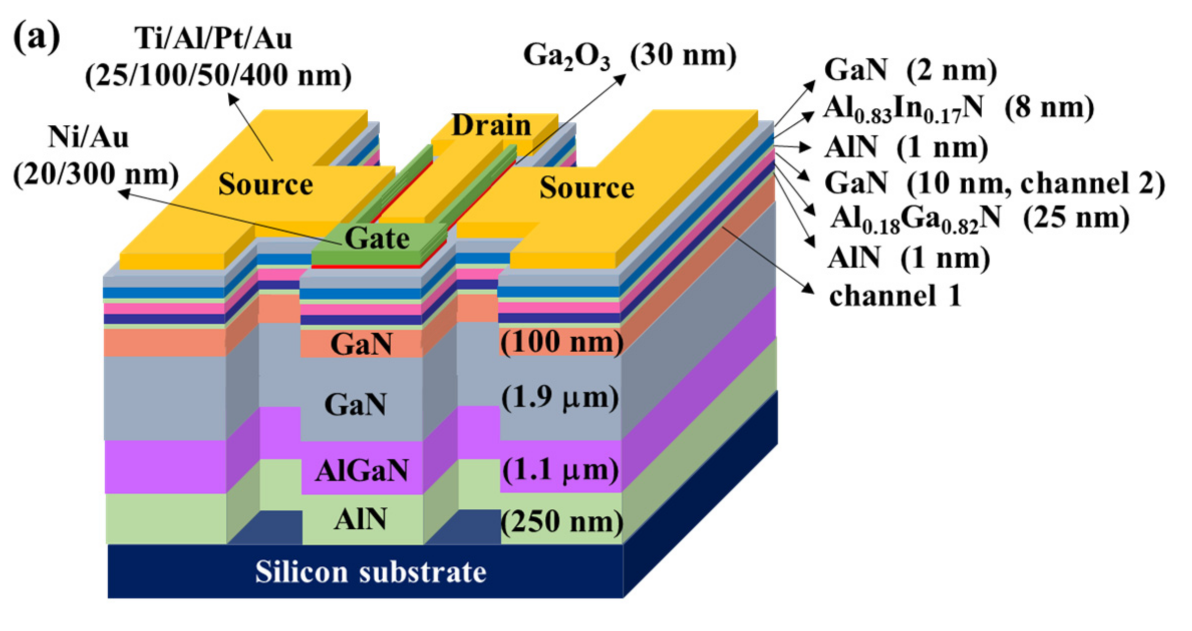
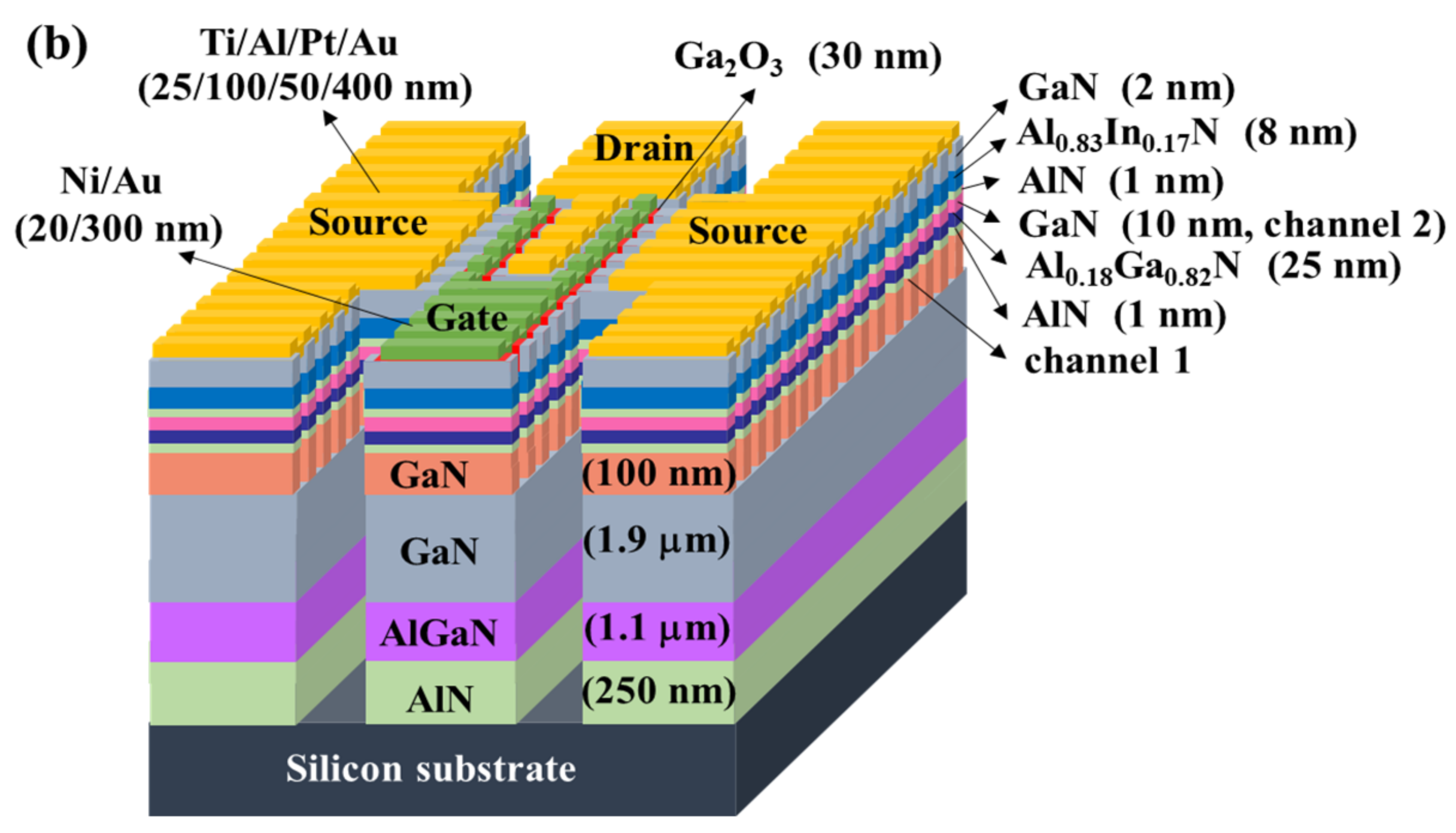
2. Epitaxial Growth and Results

A MOCVD system was utilized to grow epitaxial layers of Al0.83In0.17N/GaN/Al0.18Ga0.82N/GaN double-channel structure on Si substrate. The epitaxial structure included an AlN nucleation layer (250 nm), a graded AlGaN buffer layer (1.1 μm), a trimethylgallium (TMGa)-grown undoped GaN buffer layer (1.9 μm), a triethylgallium (TEGa)-grown GaN channel 1 layer (100 nm), an AlN spacer layer (1 nm), an Al0.18Ga0.82N barrier layer 1 (25 nm), a TEGa-grown GaN channel 2 layer (10 nm), an AlN spacer layer (1 nm), an Al0.83In0.17N barrier layer 2 (8 nm), and a GaN cap layer (2 nm). In the epitaxial growth, trimethylgallium (TMAl) and trimethylindium (TMIn) were used as the precursors for Al and In sources to grow the Al0.18Ga0.82N barrier layer and theAl0.83In0.17N barrier layer, respectively. In addition, ammonia (NH3) and hydrogen (H2) were respectively used as the nitrogen source and carrier gas for growing the 1.1-μm-thick graded AlGaN buffer layer and 1.9-μm-thick GaN buffer layer. The H2 carrier gas was replaced by nitrogen gas just before and at the end of the growth of the GaN buffer layer without growth interruption. Furthermore, by using a TEGa precursor to grow the GaN channel, the residual carbon concentration could be reduced to improve electron mobility due to the lower channel trapping [32].
Regarding the simulation of a one-dimensional (1D) Schrödinger–Poisson solver, double two-dimensional electron gas (2-DEG) channels were formed at the polarized Al0.18Ga0.82N/GaN interface and the band-discontinued lattice-matched Al0.83In0.17N/GaN interface [29]. Using a Hall measurement (Ecopia Crop., Anyang, Korea) at room temperature, the equivalent electron mobility of 1770 cm2/V-s and the equivalent sheet electron density of 1.11 × 1013 cm−2 were measured. To compare the performances of double-channel MOSHEMTs with planar channel and multiple-mesa-fin-channel array, the same epitaxial layers were used in this work.

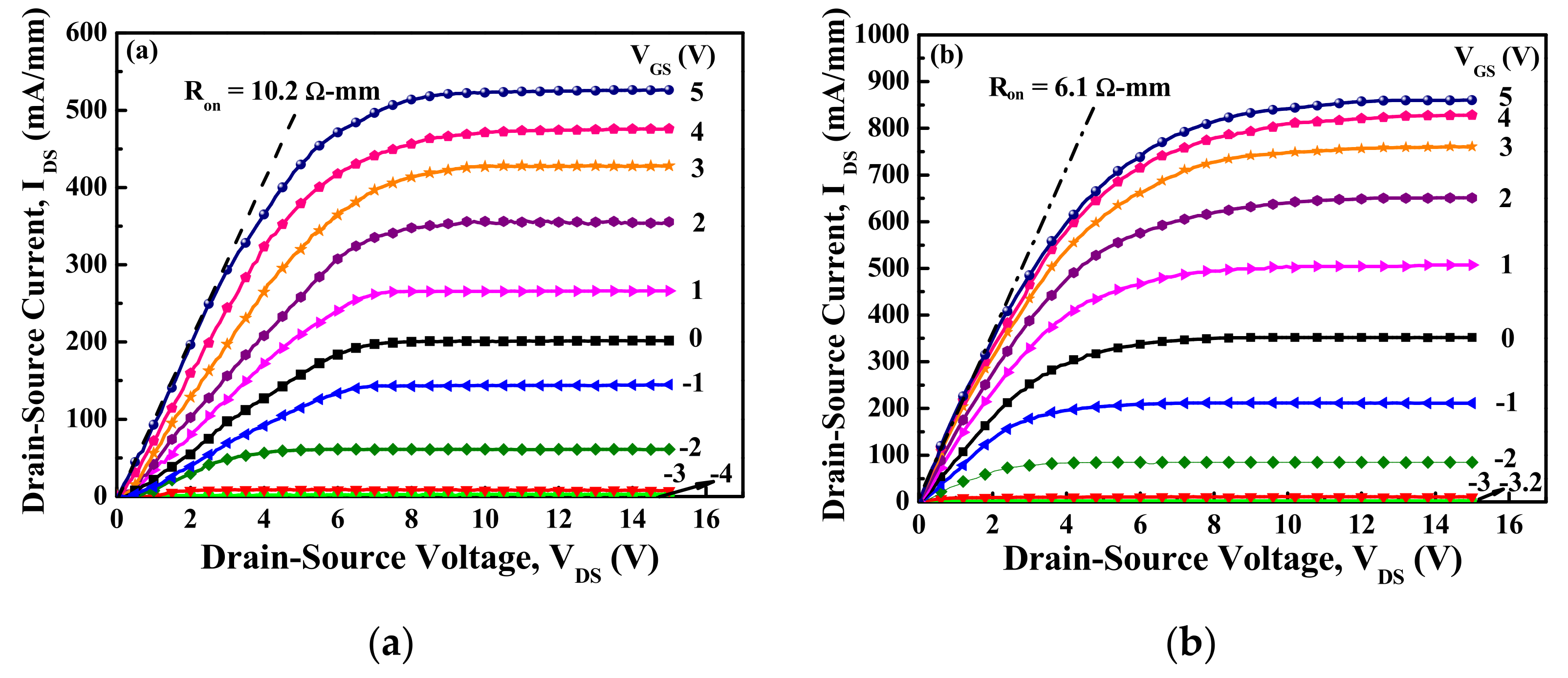
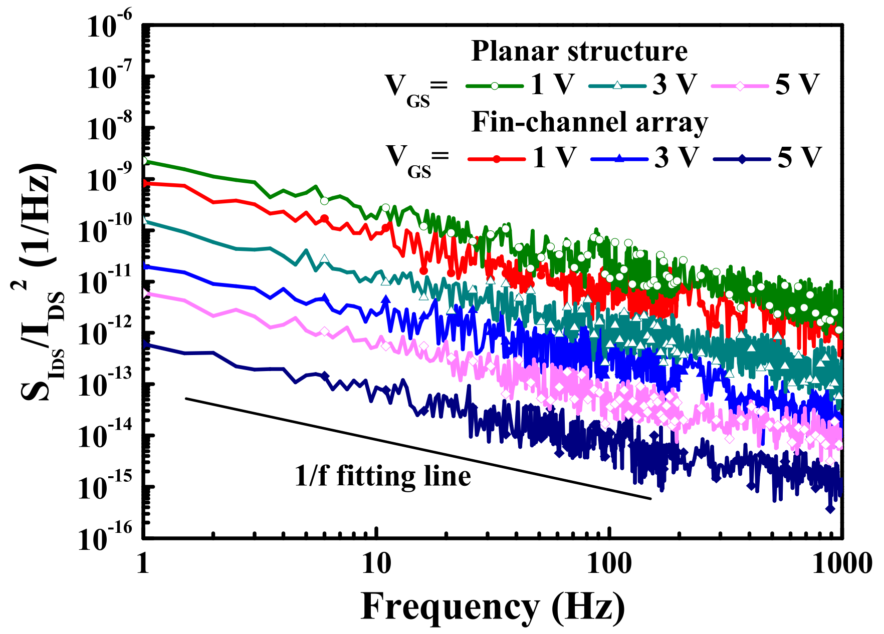
3. Results and Discussion

Figure 1a,b present the 3D schematic configuration of the double-channel Al0.83In0.17N/GaN/Al0.18Ga0.82N/GaN MOSHEMTs with planar channel and multiple-mesa-fin-channel array, respectively. Under the protection of a patterned 500-nm-thick Ni metal mask, the mesa isolation region (310 μm × 320 μm) of MOSHEMTs was etched down to Si substrate using a reactive-ion etching system with a BCl3 etchant. After removing the Ni mask using an HCl chemical solution, the sample surface was treated by an (NH4)2Sx chemical solution at 60 °C for 30 min to completely remove undesired native oxide. Using a standard photolithography system to open windows of the source electrode and drain electrode, laminated Ti/Al/Pt/Au (25/100/50/400 nm) metals were sequentially deposited and were then lifted off. By annealing the sample in a nitrogen environmental rapid-thermal annealing system at 850 °C for 1 min, an ohmic-contacted source electrode and drain electrode with a specific contact resistance of about 7.5 × 10⁶ Ω-cm2 were obtained. The separation between the source electrode and the drain electrode was 10 μm. After depositing a ZnO film (300 nm), the gate windows (length = 1 μm and width = 50 μm) placed at the central region between the source electrode and drain electrode were etched using a diluted HCl chemical solution under a photoresist mask. When the sample was repeatedly treated with a (NH4)2Sx chemical solution, a 30-nm-thick Ga2O3 film was deposited at about 80 K as the gate oxide layer using a vapor cooling condensation system. The deposition process and electrical properties of the amorphous Ga2O3 films deposited using this system were reported previously [25,33]. Prior to removing the ZnO mask, laminated Ni/Au (20/300 nm) gate metals were sequentially deposited by an electron beam evaporator. The double-channel planar Al0.83In0.17N/GaN/Al0.18Ga0.82N/GaN MOSHEMTs have a channel length of 10 μm and a channel width of 50 μm. In the same batch process, two samples of the double-channel MOSHEMTs with planar channel and multiple-mesa-fin-channel array were fabricated. Every sample included more than 200 devices. The uniformity and performance reproducibility of the MOSHEMTs were good.
In addition to the 500-nm-wide strip channel array patterned using an He-Cd laser interference photolithography system, similar fabrication processes of planar devices were utilized for fabricating devices with multiple-mesa-fin-channel array. However, within the same channel width of 50 μm, the total real channel width in the multiple-mesa-fin-channel array was 25.2 μm [29].
Using the measurement of an Agilent 4156C semiconductor parameter analyzer, Figure 2a,b respectively illustrate the typical drain–source current (IDS)−drain–source voltage (VDS) characteristics of the devices with planar channel and multiple-mesa-fin-channel array operating at various gate–source voltages (VGS). By normalizing the channel width of 50 μm, the normalized saturation drain–source current (IDSS) of the planar devices operating at VGS = 5 V and VDS = 10 V was 520.0 mA/mm, in which the real drain–source current was 26.0 mA. For the devices with multiple-mesa-fin-channel array, the IDSS was 842.7 mA/mm, in which the real drain–source current was 21.2 mA. It was worth noting that the real drain–source current in the devices with multiple-mesa-fin-channel array was less than that of the planar devices. When the on-resistance (Ron) of the devices was defined as the inverse slope of the IDS−VDS characteristics at VDS = 0 V and VGS = 5 V, the Ron = 10.2 Ω-mm of the planar devices was calculated and compared with the Ron = 6.1 Ω-mm of the devices with multiple-mesa-fin-channel array [29].
Figure 3 presents the IDS−VGS characteristics and the extrinsic transconductance (gm)−VGS characteristics of the devices with planar channel and multiple-mesa-fin-channel array operating at VDS = 10 V. In the gm−VGS characteristics shown in Figure 3, a double-hump transconductance performance was clearly observed in the planar devices; it corresponded to the effective gate modulation of the upper channel 2 and the lower channel 1, respectively. The maximum extrinsic transconductance (gmmax) of the double-hump behavior was 89.8 and 100.1 mS/mm, respectively. It was worth noting that the double-hump transconductance performance was not found in the devices with a multiple-mesa-fin-channel structure due to the better gate control capability caused by the modulation of the side-wall electrical field in the fin-channel [31]. In addition, the gmmax of 148.9 mS/mm was obtained in the single-hump transconductance. Compared with the performances of the devices with planar channel, the higher normalized saturation current, higher maximum extrinsic transconductance, and lower on-resistance in the devices with multiple-mesa-fin-channel array were contributed by the lower real drain–source current and the better heat dissipation driven by lateral heat flow within the fin-channel array [31]. If the threshold voltage (Vth) of the devices was defined as the VGS corresponding to the IDS = 1 μA/mm, the Vth of the planar devices was −3.8 V. Compared with a Vth of −3.2 V in the devices with a multiple-fin-channel array structure, the Vth was pushed toward a more positive value due to the early pinched-off effect [30,34].
An Agilent 8510C network analyzer (Agilent, CA, USA) was used to measure small-signal high-frequency performances of the MOSHEMTs. Figure 4 illustrates frequency-dependent short-circuit current gain and frequency-dependent maximum available power gain of the devices with planar channel and multiple-mesa-fin-channel array. The extrinsic unit gain cutoff frequency (fT) of 5.7 GHz and the maximum oscillation frequency (fmax) of 10.5 GHz of the planar devices were obtained. For the MOSHEMTs with multiple-mesa-fin-channel array, the fT and fmax were 6.5 GHz and 12.6 GHz, respectively [29].
In general, the low-frequency noise behaviors could be used to evaluate electron trapping and electron detrapping effects induced by traps, defects, and interface states in electronic devices [35]. The low-frequency noise characteristics of both the devices were measured using an Agilent 4156C low-noise bias supply, an HP 35670A dynamic signal analyzer, and a BTA 9812B noise analyzer. Figure 5 presents the normalized low-frequency noise power density S IDS f / I DS 2 −frequency (f) characteristics of the devices with planar channel and multiple-mesa-fin-channel array operating at VDS = 1 V. As shown in Figure 5, the normalized noise power density decreased with an increase in VGS voltage. The S IDS f / I DS 2 was about 5.4 × 10⁻¹³ Hz−1 and 8.7 × 10⁻¹⁴ Hz−1 for the devices with planar channel and multiple-mesa-fin-channel array operating at VGS = 5 V and VDS = 1 V at f = 10 Hz. Under the same operating conditions, the higher normalized noise power density in the planar devices was attributed to the larger channel area. Generally, Hooge’s coefficient α provided a useful figure-of-merit for evaluating electronic devices. The α value could be calculated as follows [36]:
α = S IDS f / I DS 2 · f · L G W G n ch V GS V th / V th
where LG = 1 μm is gate length and nch = 1.11 × 1013 cm−2 is channel electron density. In the planar devices, the gate width WG is 50 μm and the threshold voltage Vth is −3.8 V, while WG is 25.2 μm and Vth is −3.2 V in the devices with multiple-mesa-fin-channel array. The calculated α value of 7.50 × 10⁻⁵ and 6.25 × 10⁻⁶ for the MOSHEMTs with planar channel and multiple-mesa-fin-channel array operating at f = 10 Hz, VGS = 5 V, and VDS = 1 V was obtained. In addition to the result of low Hooge’s coefficient, the normalized noise power density was well fixed at 1/f. This behavior could imply that the flicker noise was the dominant noise in the devices.

4. Conclusions

Recently, planar channel structures and multiple-mesa-fin-channel array structures have been widely used for the fabrication of MOSHEMTs. In this study, to compare the performance of planar channel and multiple-mesa-fin-channel array used in double-channel MOSHEMTs, double-channel Al0.83In0.17N/GaN/Al0.18Ga0.82N/GaN epitaxial layers were grown on Si substrates using an MOCVD system. The performance comparisons of the double-channel MOSHEMTs with planar channel and multiple-mesa-fin-channel array are listed in Table 1. Compared with the performance of the double-channel MOSHEMTs with multiple-mesa-fin-channel array, double-hump transconductance behavior was observed in the double-channel planar MOSHEMTs owing to the effective gate modulation of the upper channel 2 and the lower channel 1 by the only top-side electrical field. However, in addition to the modulation of the top-side electrical field, the side-wall electric field in the multiple-mesa-fin-channel could perform at a better gate control capability. Consequently, the transconductance collapse was paved in the multiple-mesa-fin-channel. It was expected that the pavement efficiency could be enhanced by using narrower fin-channel. The extrinsic maximum double-hump transconductances of the double-channel planar MOSHEMTs were 89.8 and 100.1 mS/mm, respectively. In addition, the extrinsic maximum transconductance of the double-channel MOSHEMTs with multiple-mesa-fin-channel array was 148.9 mS/mm. Furthermore, compared with the performances of MOSHEMTs with a planar channel structure, better heat dissipation driven by the lateral heat flow in the parallel fin-channels could improve the direct-current performances and high-frequency performances [37]. The extrinsic unit gain cutoff frequency and maximum oscillation frequency of the MOSHEMTs with planar channel and multiple-mesa-fin-channel array were 5.7 and 10.5 GHz, and 6.5 and 12.6 GHz, respectively. Owing to the screening effect of the trapping probability, better noise performances were obtained in the MOSHEMTs with multiple-mesa-fin-channel array [31,38]. Hooge’s coefficient of the MOSHEMTs with planar channel and multiple-mesa-fin-channel array was 7.50 × 10⁻⁵ and 6.25 × 10⁻⁶, respectively. Although the multiple-mesa-fin-channel array exhibited superior advantages to the MOSHEMTs, its real drain–source current was less than that in the planar devices with the same channel width. Evaluating the power performances of devices with multiple-mesa-fin-channel array remains a challenging task.

Author Contributions

Conceptualization, C.-T.L.; data curation, H.-Y.L.; software and epitaxial growth, Y.-H.J. and J.-I.C. funding acquisition, C.-T.L.; investigation, H.-Y.L. and C.-T.L.; writing—original draft, C.-T.L.; writing—review and editing, H.-Y.L. and C.-T.L. All authors have read and agreed to the published version of the manuscript.

Funding

This research was funded by the Ministry of Science and Technology of Taiwan under the grants of MOST 109-2923-E-155-001, MOST 108-2221-E-006-215-MY3, and MOST 108-2221-E-155-029-MY3.

Institutional Review Board Statement

Not applicable.

Informed Consent Statement

Not applicable.

Data Availability Statement

The data presented in this study are available on request from the corresponding author.

Acknowledgments

The authors appreciate the financial support from the Ministry of Science and Technology of Taiwan.

Conflicts of Interest

The authors declare no conflict of interest.

References

  1. Roccaforte, F.; Greco, G.; Fiorenza, P.; Iucolano, F. An overview of normally-off GaN-based high electron mobility transistors. Materials 2019, 12, 1599. [Google Scholar] [CrossRef] [Green Version]
  2. Lee, H.Y.; Lin, C.H.; Wei, C.C.; Yang, J.C.; Chang, E.Y.; Lee, C.T. AlGaN/GaN enhancement-mode MOSHEMTs utilizing hybrid gate-recessed structure and ferroelectric charge trapping/storage stacked LiNbO3/HfO2/Al2O3 structure. IEEE Trans. Electron Devices 2021, 68, 3768–3774. [Google Scholar] [CrossRef]
  3. Zhang, S.; Ma, B.; Zhou, X.; Hua, Q.; Gong, J.; Liu, T.; Cui, X.; Zhu, J.; Guo, W.; Jing, L.; et al. Strain-controlled power devices as inspired by human reflex. Nat. Commun. 2020, 11, 326. [Google Scholar] [CrossRef] [PubMed]
  4. Heikman, S.; Keller, S.; Green, D.S.; DenBaars, S.P.; Mishra, U.K. High conductivity modulation doped AlGaN/GaN multiple channel heterostructures. J. Appl. Phys. 2003, 94, 5321–5325. [Google Scholar] [CrossRef]
  5. Chu, R.; Zhou, Y.; Liu, J.; Wang, D.; Chen, K.J.; Lau, K.M. AlGaN-GaN double-channel HEMTs. IEEE Trans. Electron Devices 2005, 52, 438–446. [Google Scholar] [CrossRef]
  6. Erine, C.; Ma, J.; Santoruvo, G.; Matioli, E. Multi-channel AlGaN/GaN In-plane-gate field-effect transistors. IEEE Electron Device Lett. 2020, 41, 321–324. [Google Scholar] [CrossRef]
  7. Chen, X.; Lv, D.D.; Zhang, J.F.; Zhou, H.; Ren, Z.Y.; Wang, C.; Wu, Y.; Wang, D.; Zhang, H.; Lei, Y.Y. Model of electron population and energy band diagram of multiple-channel GaN heterostructures. IEEE Trans. Electron Devices 2021, 68, 1557–1562. [Google Scholar] [CrossRef]
  8. Kamath, A.; Patil, T.; Adari, R.; Bhattacharya, I.; Ganguly, S.; Aldhaheri, R.W.; Hussain, M.A.; Saha, D. Double-channel AlGaN/GaN high electron mobility transistor with back barriers. IEEE Electron Device Lett. 2012, 33, 1690–1692. [Google Scholar] [CrossRef]
  9. Wei, J.; Liu, S.; Li, B.; Tang, X.; Lu, Y.; Liu, C.; Hua, M.; Zhang, Z.; Tang, G.; Chen, K.J. Low on-resistance normally-off GaN double-channel metal–oxide–semiconductor high-electron-mobility transistor. IEEE Electron Device Lett. 2015, 36, 1287–1290. [Google Scholar] [CrossRef]
  10. Jha, S.K.; Surya, C.; Chen, K.J.; Lau, K.M.; Jelencovic, E. Low-frequency noise properties of double channel AlGaN/GaN HEMTs. Solid-State Electron. 2008, 21, 606–611. [Google Scholar] [CrossRef]
  11. Joh, J.; Gao, F.; Palacios, T.; del Alamo, J.A. A model for the critical voltage for electrical degradation of GaN high electron mobility transistors. Microelectron. Reliab. 2010, 50, 767–773. [Google Scholar] [CrossRef]
  12. Lim, T.; Aidam, R.; Waltereit, P.; Henkel, T.; Quay, R.; Lozar, R.; Maier, T.; Kirste, L.; Ambacher, O. GaN-based submicrometer HEMTs with lattice-matched InAlGaN barrier grown by MBE. IEEE Electron Device Lett. 2010, 31, 671–673. [Google Scholar] [CrossRef]
  13. Mojaver, H.R.; Gosselin, J.L.; Valizadeh, P. Use of a bilayer lattice-matched AlInGaN barrier for improving the channel carrier confinement of enhancement-mode AlInGaN/GaN hetero-structure field-effect transistors. J. Appl. Phys. 2017, 121, 244502. [Google Scholar] [CrossRef]
  14. Shrestha, N.M.; Li, Y.; Chen, C.H.; Sanyal, I.; Tarng, J.H.; Chyi, J.I.; Samukawa, S. Design and simulation of high performance lattice matched double barrier normally off AlInGaN/GaN HEMTs. IEEE J. Electron. Devices Soc. 2020, 8, 873–878. [Google Scholar] [CrossRef]
  15. Chiou, Y.L.; Lee, C.T. Band alignment and performance improvement mechanisms of chlorine-treated ZnO-gate AlGaN/GaN metal–oxide–semiconductor high-electron mobility transistors. IEEE Trans. Electron Devices 2011, 58, 3869–3875. [Google Scholar] [CrossRef]
  16. Kim, H.S.; Kang, M.J.; Kim, J.J.; Seo, K.S.; Cha, H.Y. Effects of recessed-gate structure on AlGaN/GaN-on-SiC MIS-HEMTs with thin AlOxNy MIS gate. Materials 2020, 13, 1538. [Google Scholar] [CrossRef] [PubMed] [Green Version]
  17. Lee, C.T.; Yang, C.L.; Tseng, C.Y.; Chang, J.H.; Horng, R.H. GaN-based enhancement-mode metal-oxide-semiconductor high-electron mobility transistors using LiNbO3 ferroelectric insulator on gate-recessed structure. IEEE Trans. Electron Devices 2015, 62, 2481–2487. [Google Scholar] [CrossRef]
  18. Eller, B.S.; Yang, J.; Nemanich, R.J. Electronic surface and dielectric interface states on GaN and AlGaN. J. Vac. Sci. Technol. A 2013, 31, 050807. [Google Scholar] [CrossRef]
  19. Zhang, S.; Wei, K.; Zhang, Y.C.; Chen, X.J.; Huang, S.; Yin, H.B.; Liu, G.G.; Yuan, T.T.; Zheng, Y.K.; Wang, X.H.; et al. Well-suppressed interface states and improved transport properties of AlGaN/GaN MIS-HEMTs with PEALD SiN gate dielectric. Vacuum 2021, 191, 110359. [Google Scholar] [CrossRef]
  20. Zheng, Z.; Zhang, L.; Song, W.; Feng, S.; Xu, H.; Sun, J.; Yang, S.; Chen, T.; Wei, J.; Chen, K.J. Gallium nitride-based complementary logic integrated circuits. Nat. Electron. 2021, 4, 595–604. [Google Scholar] [CrossRef]
  21. Pearton, S.J.; Yang, J.; Cary IV, P.H.; Ren, F.; Kim, J.; Tadjer, M.J.; Mastro, M.A. A review of Ga2O3 materials, processing, and devices. Appl. Phys. Rev. 2018, 5, 011301. [Google Scholar] [CrossRef] [Green Version]
  22. Oon, H.S.; Cheong, K.Y. Recent development of gallium oxide thin film on GaN. Mater. Sci. Semicond. Process. 2013, 16, 1217–1231. [Google Scholar] [CrossRef]
  23. Shih, H.Y.; Chu, F.C.; Das, A.; Lee, C.Y.; Chen, M.J.; Lin, R.M. Atomic layer deposition of gallium oxide films as gate dielectrics in AlGaN/GaN metal–oxide–semiconductor high-electron mobility transistors. Nanoscale Res. Lett. 2016, 11, 235. [Google Scholar] [CrossRef] [Green Version]
  24. Lin, C.H.; Lee, C.T. Ga2O3-based solar-blind deep ultraviolet light-emitting diodes. J. Lumines. 2020, 224, 117326. [Google Scholar] [CrossRef]
  25. Lee, H.Y.; Chang, T.W.; Lee, C.T. AlGaN/GaN metal-oxide-semiconductor high-electron mobility transistors using Ga2O3 gate dielectric layer grown by vapor cooling condensation system. J. Electron. Mater. 2021, 50, 3748–3753. [Google Scholar] [CrossRef]
  26. Lee, H.Y.; Chang, T.W.; Chang, E.Y.; Rorsman, N.; Lee, C.T. Fabrication and characterization of GaN-based fin-channel array metal-oxide-semiconductor high-electron mobility transistors with recessed-gate and Ga2O3 gate insulator layer. IEEE J. Electron Devices Soc. 2021, 9, 393–399. [Google Scholar] [CrossRef]
  27. Chakroun, A.; Maher, M.; Al Alam, E.; Souifi, A.; Aimez, V.; Arès, R.; Jaouad, A. Optimized pre-treatment process for MOS-GaN devices passivation. IEEE Electron Device Lett. 2014, 35, 318–320. [Google Scholar] [CrossRef]
  28. Lin, Y.J.; Lee, C.T.; Chang, H.C. Changes in activation energies of donors and carrier concentration in Si-doped n-type GaN due to (NH4)2Sx treatment. Semicon. Sci. Technol. 2006, 21, 1167–1171. [Google Scholar] [CrossRef]
  29. Lee, H.Y.; Liu, D.S.; Chyi, J.I.; Chang, E.Y.; Lee, C.T. Lattice-matched AlInN/GaN/AlGaN/GaN heterostructured-double-channel metal-oxide-semiconductor high-electron mobility transistors with multiple-mesa-fin-channel array. Materials 2021, 14, 5474. [Google Scholar] [CrossRef]
  30. Lee, C.T.; Guo, J.C. Fin-gated nanochannel array gate-recessed AlGaN/GaN metal-oxide-semiconductor high-electron-mobility transistors. IEEE Trans. Electron Devices 2020, 67, 1939–1945. [Google Scholar] [CrossRef]
  31. Jia, J.J.; Lin, C.C.; Lee, C.T. Scaling effect in gate-recessed AlGaN/GaN fin-nanochannel array MOSHEMTs. IEEE Access 2020, 8, 158941–158946. [Google Scholar] [CrossRef]
  32. Sanyal, I.; Lee, Y.C.; Chyi, J.I.; Lin, K.L. High electron mobility AlInGaN/AlN/GaN heterostructures grown on 150-mm silicon substrate. SPIE Photonics West Proc. 2018, 10532, 1053213. [Google Scholar] [CrossRef]
  33. Lee, H.Y.; Lin, C.H.; Lee, C.T. Whole metal oxide p-i-n deep ultraviolet light-emitting diodes using i-Ga2O3 active emissive film. IEEE Photon. Technol. Lett. 2020, 32, 941–943. [Google Scholar] [CrossRef]
  34. Lu, B.; Matioli, E.; Palacios, T. Tri-gate normally-off GaN Power MISFET. IEEE Electron Device Lett. 2012, 33, 360–362. [Google Scholar] [CrossRef]
  35. Levinshtein, M.E.; Rumyantsev, S.L.; Gaska, R.; Yang, J.W.; Shur, M.S. AlGaN/GaN high electron mobility field effect transistors with low 1/f noise. Appl. Phys. Lett. 1998, 73, 1089–1091. [Google Scholar] [CrossRef]
  36. Hooge, F.N.; Kleinpenning, T.G.M.; Vandamme, L.K.J. Experimental studies on l/f noise, Rep. Prog. Phys. 1981, 44, 479–532. [Google Scholar] [CrossRef]
  37. Mikulics, M.; Kordoš, P.; Fox, A.; Kočan, M.; Lüth, H.; Sofer, Z.; Hardtdegen, H. Efficient heat dissipation in AlGaN/GaN heterostructure grown on silver substrate. Appl. Mater. Today 2017, 7, 134–137. [Google Scholar] [CrossRef]
  38. Vodapally, S.; Theodorou, C.G.; Bae, Y.; Ghibaudo, G.; Cristoloveanu, S.; Im, K.S.; Lee, J.H. Comparison for 1/f noise characteristics of AlGaN/GaN FinFET and planar MISHFET. IEEE Trans. Electron Devices 2017, 64, 3634–3638. [Google Scholar] [CrossRef]
Figure 1. Epitaxial structure and three-dimensional schematic configuration of double-channel MOSHEMTs with (a) planar channel and (b) multiple-mesa-fin-channel array.
Materials 15 00042 g001aMaterials 15 00042 g001b
Figure 2. Typical drain–source current−drain–source voltage characteristics of double-channel MOSHEMTs with (a) planar channel and (b) multiple-mesa-fin-channel array [29].
Materials 15 00042 g002
Figure 3. Drain–source current−gate–source voltage characteristics and extrinsic transconductance/gate–source voltage characteristics of double-channel MOSHEMTs operating at drain–source voltage of 10 V.
Materials 15 00042 g003
Figure 4. Short-circuit current gain and maximum available power gain as a function of frequency of double-channel MOSHEMTs.
Materials 15 00042 g004
Figure 5. Frequency-dependent normalized noise power density spectra of double-channel MOSHEMTs operating at drain–source voltage of 1 V.
Materials 15 00042 g005
Table 1. Performance comparisons of the double-channel MOSHEMTs with planar channel and multiple-mesa-fin-channel array.
MOSHEMTsPlanar ChannelMultiple-Mesa-Fin-Channel Array
Characteristics
Drain–source current, IDS
at VDS = 10 V and VGS = 5 V
520.0 mA/mm842.7 mA/mm
on-resistance, Ron
at VDS = 0 V and VGS = 5 V
10.2 Ω-mm6.1 Ω-mm
Transconductance, gm
at VDS = 10 V
89.8 and 100.1 mS/mm148.9 mS/mm
Threshold voltage, Vth
at IDS = 1 μA/mm
−3.8 V−3.2 V
Unit gain cutoff frequency, fT5.7 GHz6.5 GHz
Maximum oscillation frequency, fmax10.5 GHz12.6 GHz
Hooge’s coefficient, α7.50 × 1056.25 × 106
Publisher’s Note: MDPI stays neutral with regard to jurisdictional claims in published maps and institutional affiliations.

