
Artificial Anisotropy in Ge2Sb2Te5 Thin Films after Femtosecond Laser Irradiation

 , ,
, ,  , ,
, ,  and
and 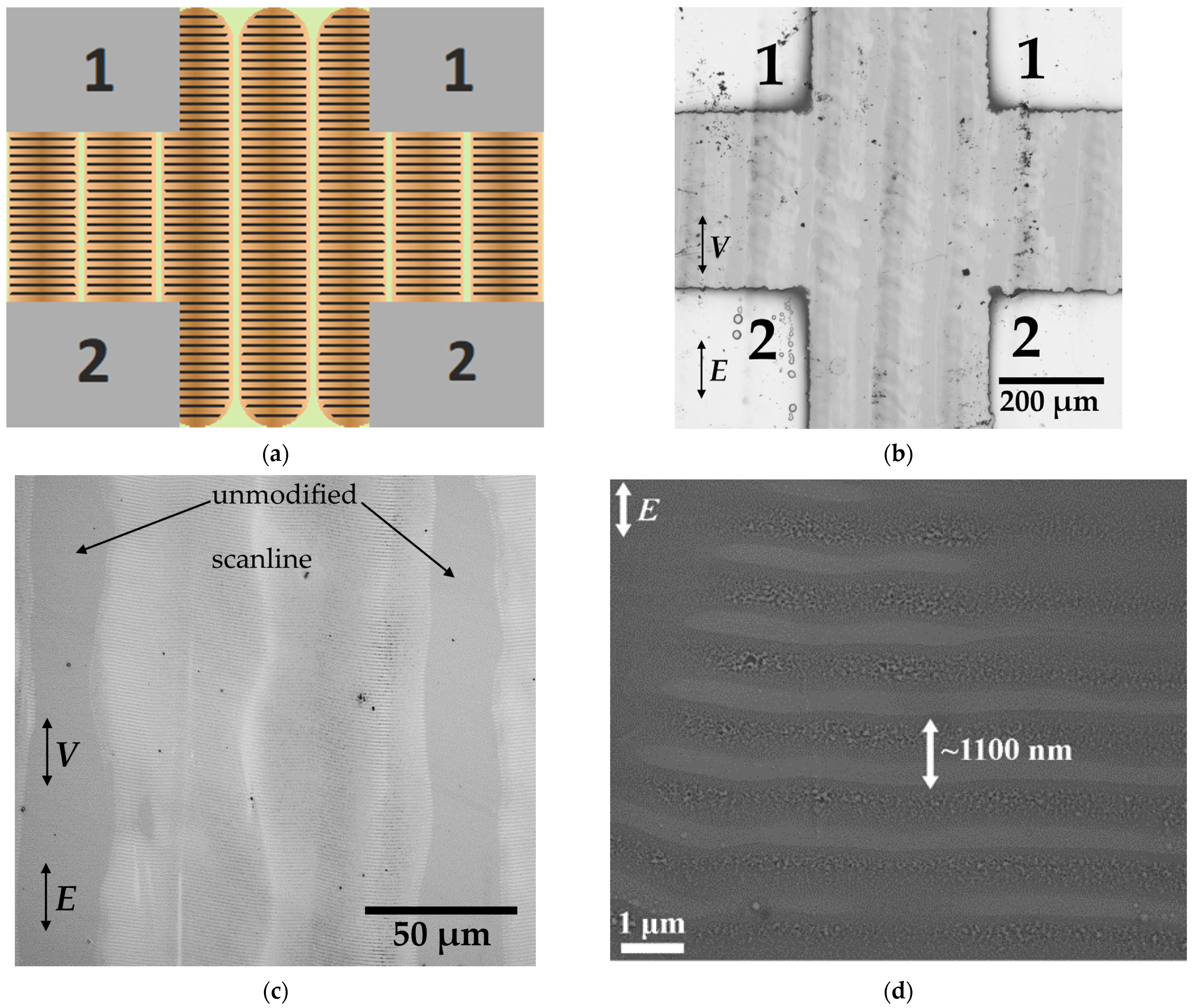
Abstract
:1. Introduction
2. Materials and Methods
3. Results and Discussion
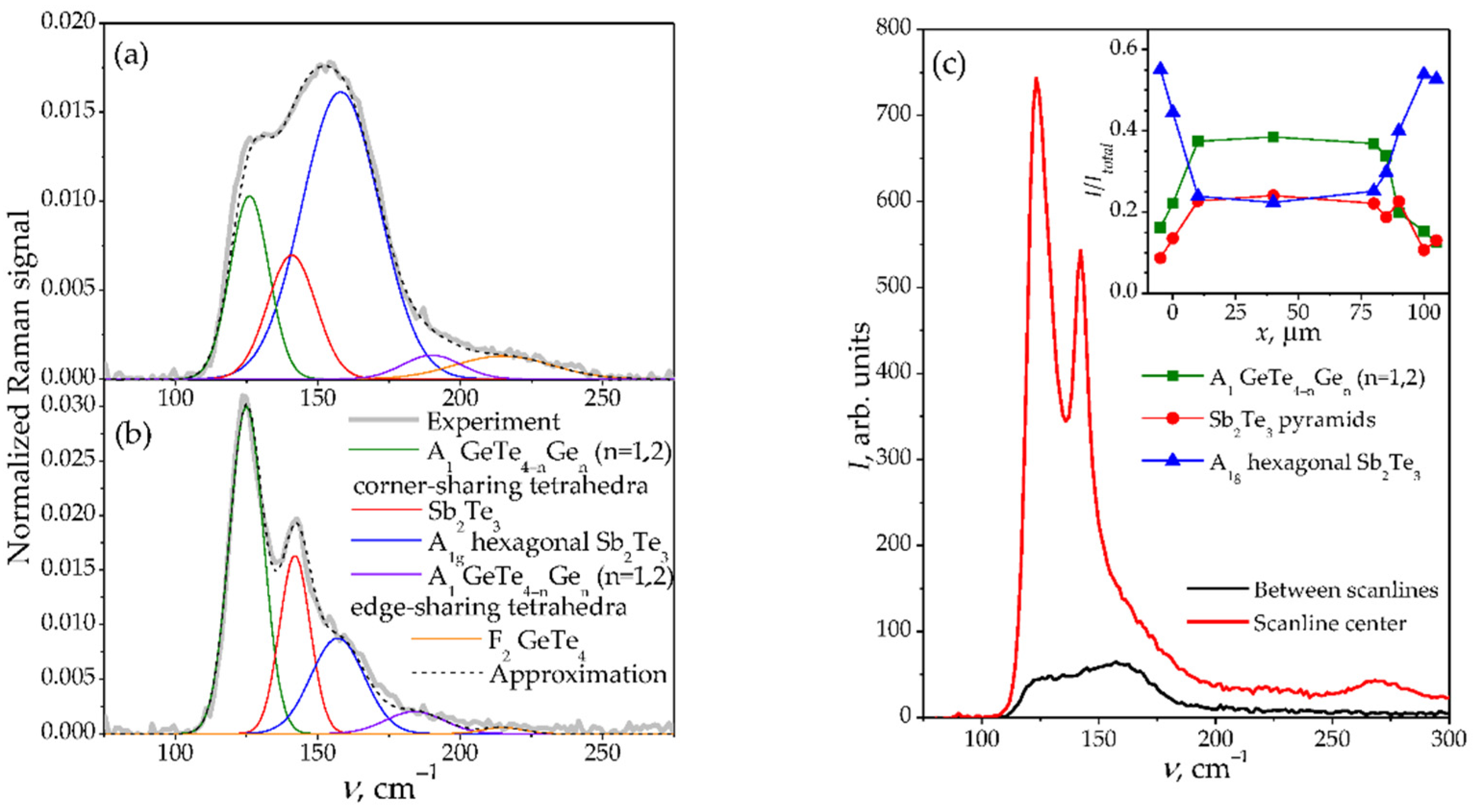
3.1. Structural Properties

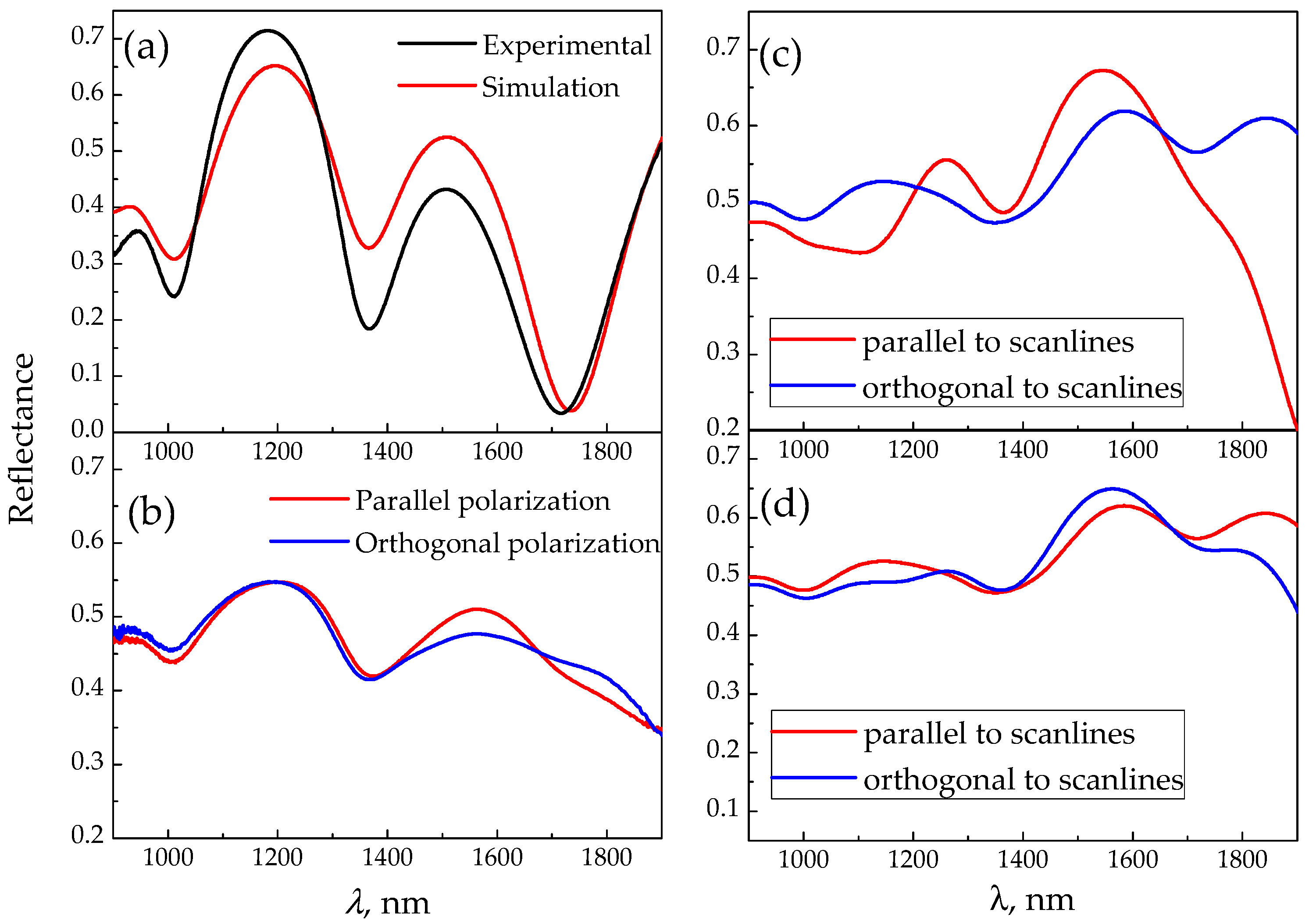
3.2. Optical Properties
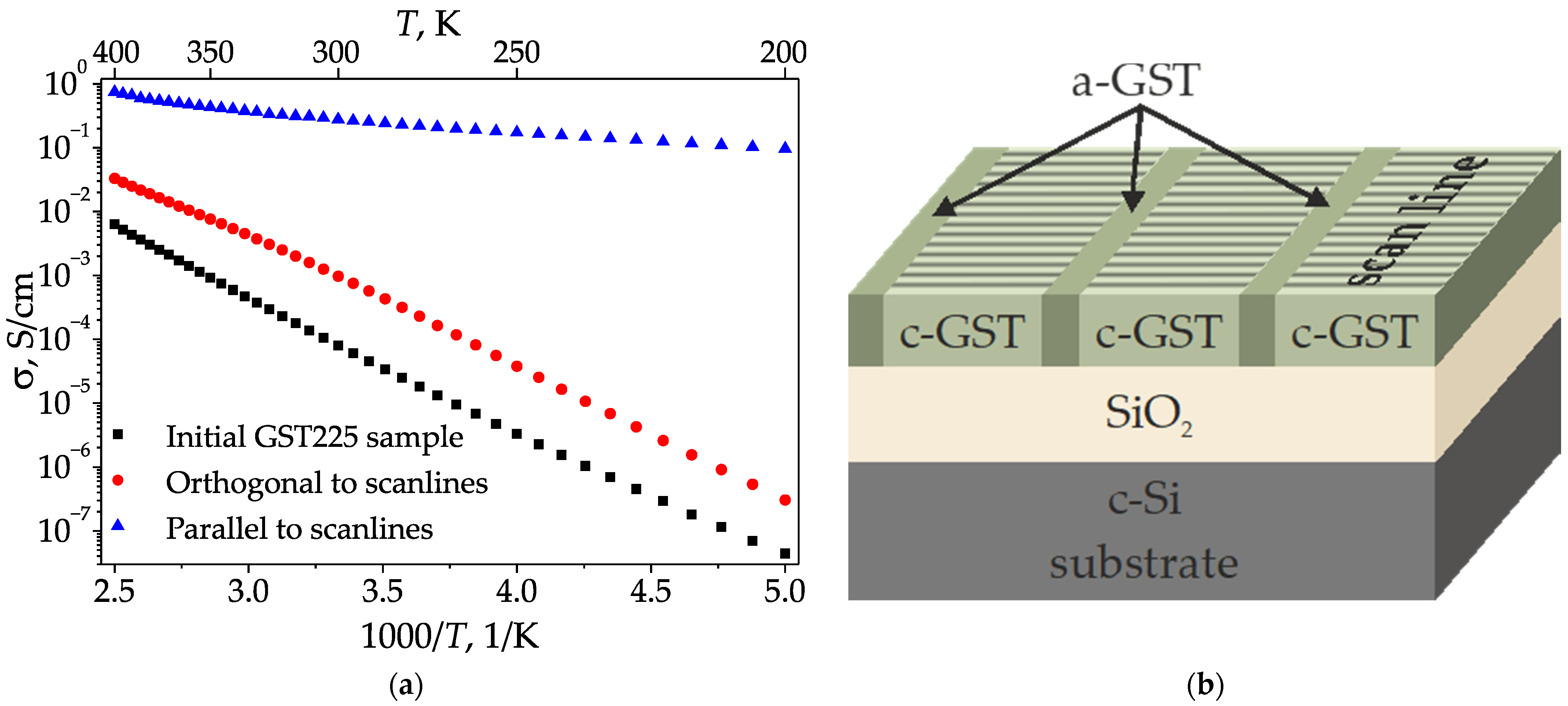
3.3. Electrophysical Properties
4. Conclusions
Author Contributions
Funding
Institutional Review Board Statement
Informed Consent Statement
Data Availability Statement
Acknowledgments
Conflicts of Interest
References
- Born, M.; Wolf, E. Form birefringence. In Principles of Optics: Electromagnetic Theory of Propagation, Interference and Diffraction of Light, 7th ed.; Cambridge University Press: Cambridge, UK, 1999; pp. 837–839. [Google Scholar] [CrossRef]
- Maxwell Garnett, J.C. Colours in metal glasses and in metallic films. Philos. Trans. R. Soc. A 1904, 203, 385–420. [Google Scholar] [CrossRef]
- Bruggeman, D.A.G. Berechnung verschiedener physikalischer konstanten von heterogenen substanzen. i. dielektrizitätskonstanten und leitfähigkeiten der mischkörper aus isotropen substanzen. Ann. Phys. 1935, 416, 636–664. [Google Scholar] [CrossRef]
- Bergman, D.J. The dielectric constant of a composite material–a problem in a classical physics. Phys. Rep. 1978, 43, 377–407. [Google Scholar] [CrossRef]
- Sarychev, A.K.; Shalaev, V.M. Electrodynamics of Metamaterials; World Scientific: Singapore, 2007; pp. 27–32. [Google Scholar]
- Ponomarenko, V.I.; Lagunov, I.M. Generalized formula for effective dielectric permeability of the medium with ellipsoidal inclusions. J. Commun. Technol. Electron. 2021, 66, 403–407. [Google Scholar] [CrossRef]
- Schmidt, D.; Schubert, M. Anisotropic Bruggeman effective medium approaches for slanted columnar thin films. J. Appl. Phys. 2013, 114, 083510. [Google Scholar] [CrossRef] [Green Version]
- Künzner, N.; Kovalev, D.; Diener, J.; Gross, E.; Timoshenko, V.Y.; Polisski, G.; Koch, F.; Fujii, M. Giant birefringence in anisotropically nanostructured silicon. Opt. Lett. 2001, 26, 1265–1267. [Google Scholar] [CrossRef] [PubMed]
- Golovan’, L.A.; Konstantinova, A.F.; Imangazieva, K.B.; Krutkova, E.Y.; Timoshenko, V.Y.; Kashkarov, P.K. Dispersion of optical anisotropy in nanostructurized silicon films. Cryst. Rep. 2004, 49, 143–148. [Google Scholar] [CrossRef]
- Gayvoronsky, V.Y.; Kopylovsky, M.A.; Gromov, Y.V.; Zabotnov, S.V.; Piskunov, N.A.; Golovan, L.A.; Timoshenko, V.Y.; Kashkarov, P.K.; Fang, G.Y.; Li, C.F. Enhancement of two-photon absorption in anisotropic mesoporous silicon. Laser Phys. Lett. 2008, 5, 894–897. [Google Scholar] [CrossRef]
- Forsh, P.A.; Martyshov, M.N.; Timoshenko, V.Y.; Kashkarov, P.K. Alternating current conductivity of anisotropically nanostructured silicon. Semiconductors 2006, 40, 471–475. [Google Scholar] [CrossRef]
- Kuladeep, R.; Sahoo, C.; Rao, D.N. Direct writing of continuous and discontinuous sub-wavelength periodic surface structures on single-crystalline silicon using femtosecond laser. Appl. Phys. Lett. 2014, 104, 222103. [Google Scholar] [CrossRef]
- Liu, P.; Jiang, L.; Hu, J.; Han, W.; Lu, Y. Direct writing anisotropy on crystalline silicon surface by linearly polarized femtosecond laser. Opt. Lett. 2013, 38, 1969–1971. [Google Scholar] [CrossRef] [PubMed]
- Dar, M.H.; Saad, N.A.; Sahoo, C.; Naraharisetty, S.R.G.; Desai, N.R. Ultrafast laser-induced reproducible nano-gratings on a molybdenum surface. Laser Phys. Lett. 2017, 14, 026101. [Google Scholar] [CrossRef]
- Xie, C.; Li, X.; Liu, K.; Zhu, M.; Qiu, R.; Zhou, Q. Direct writing of sub-wavelength ripples on silicon using femtosecond laser at high repetition rate. Appl. Surf. Sci. 2016, 360, 896–903. [Google Scholar] [CrossRef]
- Drevinskas, R.; Beresna, M.; Gecevičius, M.; Khenkin, M.; Kazanskii, A.G.; Matulaitienė, I.; Niaura, G.; Konkov, O.I.; Terukov, E.I.; Svirko, Y.P.; et al. Giant birefringence and dichroism induced by ultrafast laser pulses in hydrogenated amorphous silicon. Appl. Phys. Lett. 2015, 106, 171106. [Google Scholar] [CrossRef]
- Shuleiko, D.V.; Potemkin, F.V.; Romanov, I.A.; Parhomenko, I.N.; Pavlikov, A.V.; Presnov, D.E.; Zabotnov, S.V.; Kazanskii, A.G.; Kashkarov, P.K. Femtosecond laser pulse modification of amorphous silicon films: Control of surface anisotropy. Laser Phys. Lett. 2018, 15, 056001. [Google Scholar] [CrossRef]
- Martsinovski, G.A.; Shandybina, G.D.; Smirnov, D.S.; Zabotnov, S.V.; Golovan, L.A.; Timoshenko, V.Y.; Kashkarov, P.K. Ultrashort excitations of surface polaritons and waveguide modes in semiconductors. Opt. Spectrosc. 2008, 105, 67–72. [Google Scholar] [CrossRef]
- Ionin, A.A.; Kudryashov, S.I.; Makarov, S.V.; Rudenko, A.A.; Seleznev, L.V.; Sinitsyn, D.V.; Emel’yanov, V.I. Nonlinear optical dynamics during femtosecond laser nanostructuring of a silicon surface. Laser Phys. Lett. 2015, 12, 025902. [Google Scholar] [CrossRef]
- Bonse, J.; Gräf, S. Maxwell meets Marangoni–A review of theories on laser-induced periodic surface structures. Laser Photonics Rev. 2020, 14, 2000215. [Google Scholar] [CrossRef]
- Iida, Y.; Nikaido, S.; Miyaji, G. Sub-100-nm periodic nanostructure formation induced by short-range surface plasmon polaritons excited with few-cycle laser pulses. J. Appl. Phys. 2021, 130, 183102. [Google Scholar] [CrossRef]
- Lipatiev, A.S.; Fedotov, S.S.; Okhrimchuk, A.G.; Lotarev, S.V.; Vasetsky, A.M.; Stepko, A.A.; Shakhgildyan, G.Y.; Piyanzina, K.I.; Glebov, I.S.; Sigaev, V.N. Multilevel data writing in nanoporous glass by a few femtosecond laser pulses. Appl. Opt. 2018, 57, 978–982. [Google Scholar] [CrossRef]
- Lotarev, S.V.; Fedotov, S.S.; Kurina, A.I.; Lipatiev, A.S.; Sigaev, V.N. Ultrafast laser-induced nanogratings in sodium germanate glasses. Opt. Lett. 2019, 44, 1564–1567. [Google Scholar] [CrossRef] [PubMed]
- Fedotov, S.S.; Okhrimchuk, A.G.; Lipatiev, A.S.; Stepko, A.A.; Piyanzina, K.I.; Shahida, G.Y.; Presniakov, M.Y.; Glebov, I.S.; Lotarev, S.V.; Sigaev, V.N. 3-bit writing of information in nanoporous glass by a single sub-microsecond burst of femtosecond pulses. Opt. Lett. 2018, 43, 851–854. [Google Scholar] [CrossRef] [PubMed]
- Guo, P.; Sarangan, A.M.; Agha, I. A review of germanium-antimony-telluride phase change materials for non-volatile memories and optical modulators. Appl. Sci. 2019, 9, 530. [Google Scholar] [CrossRef] [Green Version]
- Kozyukhin, S.; Lazarenko, P.; Vorobyov, Y.; Baranchikov, A.; Glukhenkaya, V.; Smayev, M.; Sherchenkov, A.; Sybina, Y.; Polohin, A.; Sigaev, V. Laser-induced modification and formation of periodic surface structures (ripples) of amorphous GST225 phase change materials. Opt. Laser Technol. 2019, 113, 87–94. [Google Scholar] [CrossRef]
- Trofimov, P.I.; Bessonova, I.G.; Lazarenko, P.I.; Kirilenko, D.A.; Bert, N.A.; Kozyukhin, S.A.; Sinev, I.S. Rewritable and tunable laser-induced optical gratings in phase-change material films. ACS Appl. Mater. Interfaces 2021, 13, 32031–32036. [Google Scholar] [CrossRef]
- Zabotnov, S.; Kolchin, A.; Shuleiko, D.; Presnov, D.; Kaminskaya, T.; Lazarenko, P.; Glukhenkaya, V.; Kunkel, T.; Kozyukhin, S.; Kashkarov, P. Periodic relief fabrication and reversible phase transitions in amorphous Ge2Sb2Te5 thin films upon multi-pulse femtosecond irradiation. Micro 2022, 2, 5. [Google Scholar] [CrossRef]
- Karpov, V.G. Electric field driven optical recording. Appl. Phys. Lett. 2010, 97, 033505. [Google Scholar] [CrossRef]
- Němec, P.; Nazabal, V.; Moreac, A.; Gutwirth, J.; Beneš, L.; Frumar, M. Amorphous and crystallized Ge-Sb-Te thin films deposited by pulsed laser: Local structure using Raman scattering spectroscopy. Mater. Chem. Phys. 2012, 136, 935–941. [Google Scholar] [CrossRef]
- Andrikopoulos, K.S.; Yannopoulos, S.N.; Voyiatzis, G.A.; Kolobov, A.V.; Ribes, M.; Tominaga, J. Raman scattering study of the a-GeTe structure and possible mechanism for the amorphous to crystal transition. J. Phys. Condens. Matter 2006, 18, 965–979. [Google Scholar] [CrossRef] [Green Version]
- Golovchak, R.; Choi, Y.G.; Kozyukhin, S.; Chigirinsky, Y.; Kovalskiy, A.; Xiong-Skiba, P.; Trimble, J.; Pafchek, R.; Jain, H. Oxygen incorporation into GST phase-change memory matrix. App. Surf. Sci. 2015, 332, 533–541. [Google Scholar] [CrossRef]
- Wang, J.; Cui, D.; Kong, Y.; Shen, L. Unusual force constants guided distortion-triggered loss of long-range order in phase change materials. Materials 2021, 14, 3514. [Google Scholar] [CrossRef] [PubMed]
- Shportko, K.; Revutska, L.; Paiuk, O.; Baran, J.; Stronski, A.; Gubanova, A.; Venger, E. Compositional dependencies in the vibrational properties of amorphous Ge-As-Se and Ge-Sb-Te chalcogenide alloys studied by Raman spectroscopy. Opt. Mater. 2017, 73, 489–496. [Google Scholar] [CrossRef]
- Hao, Z.; Kochubei, S.A.; Popov, A.A.; Volodin, V.A. On Raman scattering cross section ratio of amorphous to nanocrystalline germanium. Solid State Commun. 2020, 313, 113897. [Google Scholar] [CrossRef]
- Lazarenko, P.I.; Vorobyov, Y.V.; Fedyanina, M.E.; Sherchenkov, A.A.; Kozyukhin, S.A.; Yakubov, A.O.; Kukin, A.V.; Sybina, Y.S.; Sagunova, I.V. Peculiarities of estimating the optical band gap of thin films of phase change memory materials. Inorg. Mater. Appl. Res. 2020, 11, 330–337. [Google Scholar] [CrossRef]
- Xu, Z.; Chen, C.; Wang, Z.; Wu, K.; Chong, H.; Ye, H. Optical constants acquisition and phase change properties of Ge2Sb2Te5 thin films based on spectroscopy. RSC Adv. 2018, 8, 21040–21046. [Google Scholar] [CrossRef] [Green Version]
- Kunkel, T.; Vorobyov, Y.; Smayev, M.; Lazarenko, P.; Veretennikov, V.; Sigaev, V.; Kozyukhin, S. Experimental observation of two-stage crystallization of Ge2Sb2Te5 amorphous thin films under the influence of a pulsed laser. J. Alloy. Compd. 2021, 851, 156924. [Google Scholar] [CrossRef]
- Vorobyov, Y.; Lazarenko, P.; Sherchenkov, A.; Vishnyakov, N.; Ermachikhin, A.; Kozyukhin, S. Kinetics of volume and surface driven crystallization in thin films. J. Phys. Condens. Matter 2020, 32, 355401. [Google Scholar] [CrossRef]
- Fedyanina, M.E.; Lazarenko, P.I.; Vorobyov, Y.V.; Kozyukhin, S.A.; Dedkova, A.A.; Yakubov, A.O.; Levitskii, V.S.; Sagunova, I.V.; Sherchenkov, A.A. Influence of the degree of crystallinity on the dispersion of the optical parameters of Ge2Sb2Te5 phase-change memory thin films. Semiconductors 2020, 54, 1775–1783. [Google Scholar] [CrossRef]
- Hass, G.; Salzberg, C.D. Optical properties of silicon monoxide in the wavelength region from 0.24 to 14.0 microns. JOSA 1954, 44, 181–187. [Google Scholar] [CrossRef]
- Kato, T.; Tanaka, K. Electronic properties of amorphous and crystalline Ge2Sb2Te5 films. Jpn. J. Appl. Phys. 2005, 44, 7340–7344. [Google Scholar] [CrossRef]
- Shuleiko, D.; Martyshov, M.; Amasev, D.; Presnov, D.; Zabotnov, S.; Golovan, L.; Kazanskii, A.; Kashkarov, P. Fabricating femtosecond laser-induced periodic surface structures with electrophysical anisotropy on amorphous silicon. Nanomaterials 2021, 11, 42. [Google Scholar] [CrossRef] [PubMed]
- Kolchin, A.V.; Shuleiko, D.V.; Zabotnov, S.V.; Golovan, L.A.; Presnov, D.E.; Kaminskaya, T.P.; Lazarenko, P.I.; Kozyukhin, S.A.; Kashkarov, P.K. Formation of periodic surface structures in multilayer amorphous Ge2Sb2Te5 thin films irradiated by femtosecond laser pulses. J. Phys. Conf. Ser. 2020, 1686, 012006. [Google Scholar] [CrossRef]


Publisher’s Note: MDPI stays neutral with regard to jurisdictional claims in published maps and institutional affiliations. |
© 2022 by the authors. Licensee MDPI, Basel, Switzerland. This article is an open access article distributed under the terms and conditions of the Creative Commons Attribution (CC BY) license (https://creativecommons.org/licenses/by/4.0/).
Share and Cite
Kolchin, A.; Shuleiko, D.; Martyshov, M.; Efimova, A.; Golovan, L.; Presnov, D.; Kunkel, T.; Glukhenkaya, V.; Lazarenko, P.; Kashkarov, P.; et al. Artificial Anisotropy in Ge2Sb2Te5 Thin Films after Femtosecond Laser Irradiation. Materials 2022, 15, 3499. https://doi.org/10.3390/ma15103499
Kolchin A, Shuleiko D, Martyshov M, Efimova A, Golovan L, Presnov D, Kunkel T, Glukhenkaya V, Lazarenko P, Kashkarov P, et al. Artificial Anisotropy in Ge2Sb2Te5 Thin Films after Femtosecond Laser Irradiation. Materials. 2022; 15(10):3499. https://doi.org/10.3390/ma15103499
Chicago/Turabian StyleKolchin, Aleksandr, Dmitrii Shuleiko, Mikhail Martyshov, Aleksandra Efimova, Leonid Golovan, Denis Presnov, Tatiana Kunkel, Victoriia Glukhenkaya, Petr Lazarenko, Pavel Kashkarov, and et al. 2022. "Artificial Anisotropy in Ge2Sb2Te5 Thin Films after Femtosecond Laser Irradiation" Materials 15, no. 10: 3499. https://doi.org/10.3390/ma15103499
APA StyleKolchin, A., Shuleiko, D., Martyshov, M., Efimova, A., Golovan, L., Presnov, D., Kunkel, T., Glukhenkaya, V., Lazarenko, P., Kashkarov, P., Zabotnov, S., & Kozyukhin, S. (2022). Artificial Anisotropy in Ge2Sb2Te5 Thin Films after Femtosecond Laser Irradiation. Materials, 15(10), 3499. https://doi.org/10.3390/ma15103499