Article

Reducing Threading Dislocations of Single-Crystal Diamond via In Situ Tungsten Incorporation

1
Ministry Education Key Laboratory of Physical Electronics and Devices, School of Electronic Science and Engineering, Xi’an Jiaotong University, Xi’an 710049, China
2
Key Laboratory of the Ministry of Education, International Center for Dielectric Research, School of Electronic Science and Engineering, Xi’an Jiaotong University, Xi’an 710049, China
3
School of Materials Science & Engineering, Taiyuan University of Science & Technology, Taiyuan 030024, China
4
National Key Laboratory of Application Specific Integrated Circuit, Hebei Semiconductor Research Institute, Shijiazhuang 050051, China
*
Authors to whom correspondence should be addressed.
Materials 2022, 15(2), 444; https://doi.org/10.3390/ma15020444
Submission received: 17 November 2021 / Revised: 23 December 2021 / Accepted: 5 January 2022 / Published: 7 January 2022
(This article belongs to the Special Issue Diamond Material and Its Applications)

Abstract

:
A lower dislocation density substrate is essential for realizing high performance in single-crystal diamond electronic devices. The in-situ tungsten-incorporated homoepitaxial diamond by introducing tungsten hexacarbonyl has been proposed. A 3 × 3 × 0.5 mm3 high-pressure, high-temperature (001) diamond substrate was cut into four pieces with controlled experiments. The deposition of tungsten-incorporated diamond changed the atomic arrangement of the original diamond defects so that the propagation of internal dislocations could be inhibited. The SEM images showed that the etching pits density was significantly decreased from 2.8 × 105 cm−2 to 2.5 × 103 cm−2. The reduction of XRD and Raman spectroscopy FWHM proved that the double-layer tungsten-incorporated diamond has a significant effect on improving the crystal quality of diamond bulk. These results show the evident impact of in situ tungsten-incorporated growth on improving crystal quality and inhibiting the dislocations propagation of homoepitaxial diamond, which is of importance for high-quality diamond growth.

1. Introduction

In the past 10–20 years, the progress of semiconductor materials has created many updated science technologies, such as 5G communication, artificial intelligence, quantum information, and power devices. Of all the semiconductor materials, diamond possesses a wide band gap (5.5 eV), high thermal conductivity (2200 W/mK), high breakdown voltage (10 MV/cm), high carriers’ mobility, high saturation velocity of holes (1.5 × 107 cm/s), and high Johnson’s and Baliga’s figure of merit, making it a promising semiconductor material for next-generation devices [1,2,3,4,5,6,7,8]. However, the existence of defects located in diamond substrates leads to a reduction in the material properties. Defects in diamond include point defects [9], stacking faults (SFs) [10], and threading dislocations (TDs) [11]. Point defects are mainly contained in nitrogen-vacancy centers (NV0, NV) [12], silicon vacancy centers (SiV) [13], and hydrogen-related defects [14]. Owing to mechanical damage, SFs usually start from the substrate and then penetrate through the growth layer [15]. It can be removed by chemical mechanical polishing [16]. The dislocation density quantitatively shows the number of defects per unit area. For Ⅱa natural diamond crystal, the dislocation density is 108–109 cm−2, which is three to four orders higher than that of synthetic homoepitaxial diamond (104–106 cm−2) [17]. Compared to the SFs, the threading dislocations are the main reason for the deterioration of electronic devices performance (i.e., leakage current and breakdown voltage) based on single crystal diamond, especially the dislocations-induced non-linear charge transport mechanisms [18]. Numerous studies have focused on reducing diamond dislocation density. Naamoun et al. revealed a selective masking strategy aiming at preventing threading dislocations propagation by Pt particles. Then, chemical vapor deposition diamond was carried out after a metallic mask [19]. Repeating this procedure several times could lead to a large decrease in the dislocations. Another way to decrease the dislocation density in single crystal diamond is epitaxial lateral overgrowth (ELO). Tallaire et al. proposed a diamond ELO with a large macroscopic hole. The dislocation density in the center was calculated to be approximately 2 × 103 cm−2 [20]. Li et al. used a two-step ELO process on an Ib diamond (100) substrate, which combined inductively coupled plasma (ICP) etching and the sputtering of Mo/Pd stripes. The etching pit density was an order of magnitude lower in the two-step ELO layer [21]. Tang et al. proposed a method for high-quality diamond by heteroepitaxial lateral overgrowth. With Au stripe masks on the diamond surface, the stress decreased significantly, and the dislocation density was below 108 cm−2 [22]. Kim et al. fabricated a one-inch free-standing heteroepitaxial (001) diamond with a dislocation density of 1.4 × 107 cm−2 [23]. Mehmel et al. used micrometric laser-pierced hole arrays to reduce dislocation densities [24]. For diamond thick layer growth, Tsubouchi et al. investigated the microstructures of grown-in threading dislocation bundles in four different growth directions using cross-sectional TEM [25]. Achard et al. found that thick diamond grown on a pyramidal-shaped substrate can lead to dislocation bending and further studied the growth of thick crystals with low dislocation density [9,26]. However, the process of current research is complicated and requires several epitaxial growths, photolithography, sputtering, and etching, and the dislocation density can only be reduced by one to two orders of magnitude. Ohmagari et al. researched homoepitaxial diamond film growth by hot-filament chemical vapor deposition (HFCVD) accompanying tungsten (W) incorporations from heated metal wires. A large reduction in threading dislocation from 2 × 10⁶ to 3 × 104 cm−2 was demonstrated by W impurities [27]. However, the diamond films were fabricated in two independent deposition systems, which may lead to new impurities during the growth interval.
In this work, a tungsten-incorporated single-crystal diamond multilayer structure, which could effectively reduce dislocation propagation, was fabricated. At the beginning of the diamond growth, a tungsten precursor was introduced to form a W-C atom-level connection. Then, the tungsten precursor was turned off, and the homoepitaxial diamond continued to grow. The combination of W and C atoms at defects was used to change the arrangement of C atoms at defects, so that C atoms could return to the diamond lattice position, and the propagation of defects (especially dislocations) to diamond films could be inhibited, thereby providing an effective method to reduce the dislocations of homoepitaxial diamond. Compared to the previous studies, the advantage introduced in this work is that the incorporation of W atoms occurs in situ (i.e., in the same deposition chamber) and does not require additional process steps, which would degrade the film quality. This study may put forward a valuable method for growing high-quality and low-defect density single crystal diamond by inhibiting the dislocations propagation, which could be applied in diamond power devices.

2. Experimental

The homoepitaxial growth of tungsten-incorporated diamond was fabricated by microwave plasma chemical vapor deposition (MPCVD, AX5250S Seki Technotron Corp. Koto, Japan) on (100)-oriented synthetic high-pressure high-temperature (HPHT) substrate (3 × 3 × 0.5 mm3) with the offset angle less than 2°. The substrate was cut into four 1.5 × 1.5 × 0.5 mm3 crystals for comparative experiment. The precursor was tungsten hexacarbonyl (W(CO)6), which was incorporated into the chamber with hydrogen as the carrier gas. The purity of this solid tungsten source was 99.999%, and the heating temperature is 60 °C. The flow rate was 1.5 sccm, and the W/H ratio, CH4 concentration (C/H ratio), and N2 concentration (N/H ratio) were 0.3%, 6–7%, and 0.001%, respectively. The deposition temperature and power were 1100 °C and 3800 W, respectively, and the chamber pressure was 160 mbar. The thickness of the tungsten-incorporated layer was 3 μm. Next, the intrinsic diamond was grown in an in situ chamber. The O2 concentration (O/H ratio) was 0.5–1%, the deposition temperature was 1050 °C, and the C/H, N/H, and chamber pressures were maintained at the same level. After growth, H2/O2 (500/5 sccm) plasma was applied to the samples to form etching pits. The etching temperature was 1000 °C, and the duration was 30 min.
The dark current was tested by a semiconductor characterization system (Keithley 4200). A 6-circle XRD (SmartLab, Rigaku, Tokyo, Japan) system was used to test the crystallinity of the diamond containing both the substrate and epitaxial layers [28]. The confocal micro-Raman spectrometer (Renishaw inVia, New Mills, UK) was used to evaluate the diamond defect structures. The laser is a 532 nm Nd: sapphire with laser power of 1%, the excitation power is 50 mW, and the resolution of the spectrometer in the horizontal and depth directions is 1 μm. The microstructure and dislocation densities (dislocations crossing unit area) were observed using an SEM (Gemini SEM 500, Zeiss, Dresden, Germany). The concentrations of tungsten and nitrogen impurities were determined using SIMS (Cameca 4F, Gennevilliers, France).

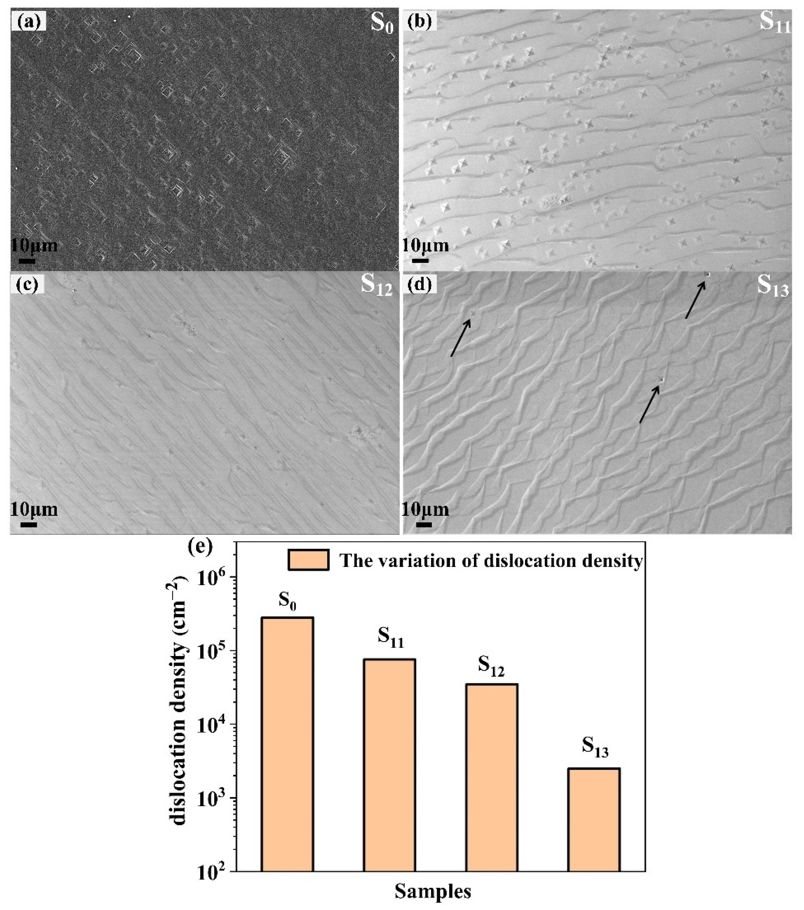
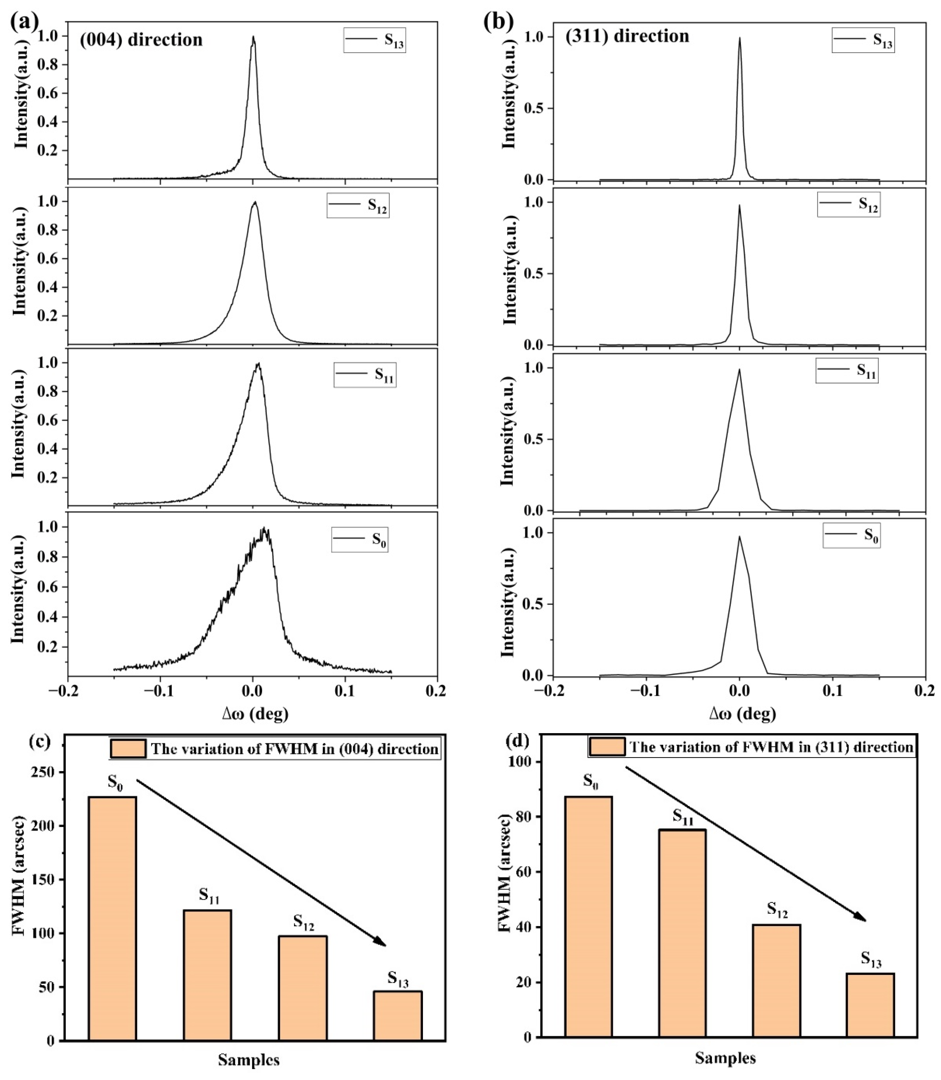
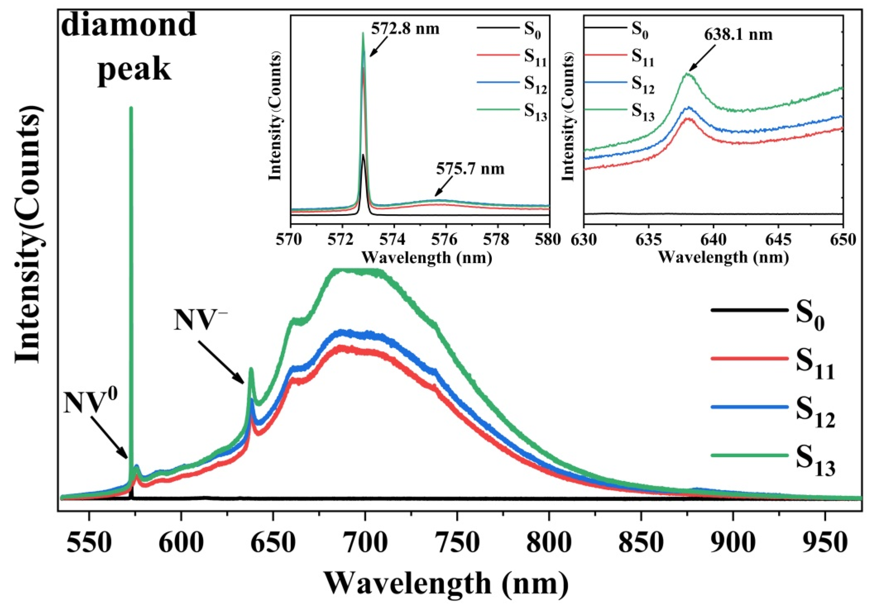
3. Results and Discussion

The variation of film structures is shown in Figure 1a. S0 was the HPHT substrate, which was set as a controlled sample. For S11, a 10 μm intrinsic diamond was grown on the substrate. Single and double layers of tungsten-incorporated diamond (3 μm) were deposited for S12 and S13, respectively. The W concentration was measured by SIMS with another controlled sample (10 μm), which was shown in Figure 1b. The W concentration was uniform in diamond bulks, showing the good consistency of approximately 2 × 10¹⁶/cm3 in the whole film, which was two orders of magnitude lower than the present work (1018/cm3) [27].
Meanwhile, the nitrogen concentration was close to the 1016 cm−3 (shown in the inset of Figure 1b), which could come from unintentional nitrogen in the chamber. Furthermore, in order to explore the carrier’s transportation characteristics of tungsten-incorporated diamond, the I–V characteristics of intrinsic diamond (S11) and double-layer tungsten-incorporated diamond (S13) under dark condition are shown in Figure 1c. It was obvious that the dark currents of the two samples almost maintain consistency. When the voltage was applied at 40V, the relatively low dark current of S11 and S13 are 6.07 × 10⁻¹⁰ A and 6.87 × 10⁻¹⁰ A, respectively, indicating that the carrier’s transportation was not changed with the introduction of tungsten-incorporated diamond. The N concentration in tungsten incorporated diamond was also tested by SIMS (shown in supplementary Figure S1), and the average value was close to 1016 cm–3.
The effect of tungsten-incorporated diamond layer on the dislocation reduction could be revealed directly from the SEM images after H2/O2 etching. Figure 2a–d showed the morphology of the four samples under the same magnification, and the square-pits along (110) directions can be originated from dislocations [19]. Compared to the samples (S11, S12, and S13) deposited in MPCVD, the etching pits density of S0 was the highest, indicating that the HPHT diamond substrate contained many defects. To be specific, Figure 2b–d showed the step flow morphology of homoepitaxial diamond [29]. The trend of dislocation density is shown in Figure 2e. The dislocation density of S0 and S11 stayed at the same level (2.8 × 105 cm−2 and 7.6 × 104 cm−2, respectively), which meant that the intrinsic diamond layer could not effectively stop the propagation of dislocations. Furthermore, the etching pits densities were reduced significantly in S12 and S13. Particularly, only three pits were observed in S13, and the dislocation densities were 3.5 × 104 cm−2 and 2.5 × 103 cm−2, respectively, which proved an effective method of reducing dislocation density.
Furthermore, tungsten incorporation will also improve the crystal quality of diamond. The crystallinity of the four samples is shown in Figure 3, and the ω scans were obtained in the diamond (004) symmetric diffraction and (311) asymmetric diffraction, which represented the decent single crystal characteristics. In Figure 3a, stronger asymmetric broader peaks (S0 and S11) have been detected, which are attributed to the defects in the diamond lattice. Meanwhile, the well-performed XRD rocking curves of S12 and S13 with the narrower peak corresponded to tungsten-incorporated diamond. The full widths at half maximum (FWHM) in (004) and (311) reflections (shown in Figure 3c,d) of S0 extracted from the ω-scan were 226.8 and 87.3 arcsec, representing the worse crystallinity of the HPHT substrate [30,31]. Then, the diffraction peaks of S11 to S13 were narrowed after intrinsic diamond and tungsten-incorporated diamond deposition, and the FWHM (004) of S11 to S13 were 121.3, 97.2, and 46.0 arcsec respectively. While the FWHM (311) of S11 to S13 were 75.24, 40.89, and 23.22 arcsec respectively. As we mentioned before, the substrates were cut from the same 3 × 3 mm2 HPHT substrate for controlled experiments, indicating that the crystallinity of the whole diamond bulk was improved by tungsten-incorporated diamond.
Additionally, in order to evaluate the origin of defects in tungsten-incorporated diamond, the research of photoluminescence (PL) spectra was carried out as well as an investigation of correlation of the defect to Raman spectroscopy peak width and shift. Figure 4 showed the normalized intensity of PL spectra among four combined samples. The insets showed the amplification of the 570–580 nm and 630–650 nm wavelength. The resolution of the spectrometer in the horizontal and depth directions was 1 μm, so that the PL and Raman measurements were made for individual layers. The sharp Raman line at 572.8 nm indicated the high quality of diamond. There were two relatively strong zero phonon lines (ZPL) at 575.7 nm and 638.1 nm, which represented NV0 and NV [32]. Before growth, there was no NV center in the substrate. The obvious NV0 and NV characteristic peaks were detected after homoepitaxial diamond deposition (S11 to S13), illustrating that more vacancies were introduced during tungsten-incorporated diamond growth. The possible reasons were as follows: under high-temperature and plasma conditions, the C atoms in the diamond lattice were partially separated from the original lattice and reacted with W atoms to form vacancies. Then, NV centers in diamond (nitrogen concentration was about 1016 cm−3, which was observed in the inset of Figure 1b) were formed with the movement of vacancies at high temperatures [12]. Furthermore, NV centers were stronger in the S12 and S13 samples, which meant that the TID layer could effectively enhance the density of NV centers, especially for NV [33].
To further discussion, the variation of Raman spectroscopy with four samples are shown in Figure 5. All images showed the characteristics peaks of diamond SP3 orbital hybridization. Overall, we could see clearly that the peak of S0 showed almost consistency with intrinsic diamond (1332 cm−1). However, the shift of peaks that occurred in S11, S12, and S13 reached 0.47, 0.51, and 0.9 cm−1, respectively, which could probably be caused by nitrogen addition. The research by Bergman et al. illustrated that the positive shift in Raman peak was attributed to the nitrogen-induced expansion stress [34]. As mentioned in Figure 4, the intensity of NV centers (NV0 and NV) are strongest in S13, which is in correlation with the largest shift of Raman peak. In addition, it is inferred that with the incorporation of W, the recombination of W and C atoms will produce new vacancies, which probably lead to the shift of Raman peak as well. Furthermore, the variation of FWHM in Raman spectroscopy was usually used to characterize the crystal quality in the diamond; i.e., a narrow FWHM corresponded to better crystallinity and lower defects density [35], which was also mentioned in the explanations of Figure 5. The FWHM values of S0, S11, S12, and S13 are 5.27, 5.20, 5.14, and 4.97 cm−1, respectively. As we have already known, the line width of Raman was closely related to the defects in diamond lattice. The nitrogen defects were extensive in the HPHT substrate, which would disturb the crystal lattice and induce infrared absorption in the one-phonon region. Then, the mean free path of phonons became shorter as they experienced additional scattering on nitrogen defects, leading to the widening of Raman peaks [36]. Therefore, the FWHM of S0 was the largest. After the MPCVD growth of intrinsic diamond and a tungsten-incorporated diamond layer, the narrower of line width in S11 to S13 could probably be attributed to the following reasons: the reduction of dislocation density by introducing the tungsten-incorporated diamond layer, and the probability of a phonon scattering on nitrogen defects was stronger than zero phonon lines (NV0 and NV).

4. Conclusions

In this paper, a low dislocation density tungsten-incorporated diamond growth by in situ microwave plasma chemical vapor deposition has been proposed. The tungsten hexacarbonyl is introduced into the reaction chamber with hydrogen as a carrier gas. As a result, tungsten atoms replace the defects in the diamond lattice and repair the lattice mismatch at the defects, inhibiting the propagation of dislocations. The dislocation densities of the tungsten-incorporated diamond were reduced by two orders of magnitude (2.8 × 105 cm−2 vs. 2.5 × 103 cm−2). As a result of the lower concentration of tungsten (2 × 1016 cm−3), the carrier transport characteristics of diamond do not change by testing the I–V characteristics of S11 and S13 under dark condition. The FWHM of the XRD ω-scan is 23.22 arcsec in the (311) direction, indicating that the crystal quality of tungsten-incorporated diamond could reach the level of synthetic Ib diamond. This study provides a simplified in situ method for high-quality, low-defect density homoepitaxial diamond growth, which is of great importance in diamond electronic devices. Further studies could be extended to the tungsten incorporation to control the concentration, electron spin, and fluorescence lifetime of NV centers in diamond, which makes diamond NV centers the potential applications in quantum information technology.

Supplementary Materials

The following supporting information can be downloaded at: https://www.mdpi.com/article/10.3390/ma15020444/s1, Figure S1. N concentration in TID tested by SIMS.

Author Contributions

Conceptualization, R.W. and H.-X.W.; Methodology, R.W.; Formal analysis, R.W. and Q.W.; Investigation, J.S. and X.Y.; Software, F.L.; Data curation, X.Y.; Project administration, W.W.; Funding acquisition, C.Y.; Resources, K.W.; Visualization, H.-X.W.; Writing—original draft, R.W.; Supervision, G.N. and H.-X.W.; Writing—review and editing, G.N., W.W., K.W., C.Y. and H.-X.W. All authors have read and agreed to the published version of the manuscript.

Funding

This work was supported by the National Key Research and Development Program of China (Grant No. 2018YFE0125900), the National Natural Science Foundation of China (Grant No. 61627812, 61804122 and 62074127), and the Key R&D Program of Shaanxi Province of China (2020GY-271).

Institutional Review Board Statement

Not applicable.

Informed Consent Statement

Not applicable.

Data Availability Statement

Data available on request due to restrictions, e.g., privacy or ethical.

Acknowledgments

We would like to thank Master Ren at Taiyuan University of Science and Technology for supporting the PL experiment.

Conflicts of Interest

The authors declare no conflict of interest.

References

  1. Zhang, Z.; Sang, L.; Huang, J.; Wang, L.; Koizumi, S.; Liao, M. Tailoring the magnetic properties of galfenol film grown on single-crystal diamond. J. Alloys Compd. 2021, 858, 157683. [Google Scholar] [CrossRef]
  2. Kitabayashi, Y.; Kudo, T.; Tsuboi, H.; Yamada, T.; Xu, D.; Shibata, M.; Matsumura, D.; Hayashi, Y.; Syamsul, M.; Inaba, M.; et al. Normally-Off C-H Diamond MOSFETs with Partial C-O Channel Achieving 2-kV Breakdown Voltage. IEEE Electron Device Lett. 2017, 38, 363–366. [Google Scholar] [CrossRef]
  3. Yang, N.; Yu, S.; MacPherson, J.V.; Einaga, Y.; Zhao, H.; Zhao, G.; Swain, G.M.; Jiang, X. Conductive diamond: Synthesis, properties, and electrochemical applications. Chem. Soc. Rev. 2019, 48, 157–204. [Google Scholar] [CrossRef]
  4. Wang, K.; Guo, R.; Ding, S.; Wang, H.; Tian, Y.; Wang, Y. Temperature dependence of optical centres in ultrapure diamond after 200 keV electron irradiation. J. Phys. D Appl. Phys. 2020, 53, 135303. [Google Scholar] [CrossRef]
  5. Wei, Q.; Zhang, X.; Lin, F.; Wang, R.; Chen, G.; Wang, H. Fabrication of a Micron-Scale Three-Dimensional. Materials 2021, 14, 3006. [Google Scholar] [CrossRef] [PubMed]
  6. Shao, G.; Wang, J.; Zhang, S.; Wang, Y.; Wang, W.; Wang, H.X. Surface morphology and microstructure evolution of single crystal diamond during different homoepitaxial growth stages. Materials 2021, 14, 5964. [Google Scholar] [CrossRef] [PubMed]
  7. Isberg, J.; Hammersberg, J.; Johansson, E.; Wikström, T.; Twitchen, D.J.; Whitehead, A.J.; Coe, S.E.; Scarsbrook, G.A. High carrier mobility in single-crystal plasma-deposited diamond. Science 2002, 297, 1670–1672. [Google Scholar] [CrossRef] [PubMed]
  8. Pernegger, H.; Roe, S.; Weilhammer, P.; Eremin, V.; Frais-Kölbl, H.; Griesmayer, E.; Kagan, H.; Schnetzer, S.; Stone, R.; Trischuk, W.; et al. Charge-carrier properties in synthetic single-crystal diamond measured with the transient-current technique. J. Appl. Phys. 2005, 97, 073704. [Google Scholar] [CrossRef] [Green Version]
  9. Barjon, J.; Jomard, F.; Tallaire, A.; Achard, J.; Silva, F. Determination of exciton diffusion lengths in isotopically engineered diamond junctions. Appl. Phys. Lett. 2012, 100, 122107. [Google Scholar] [CrossRef]
  10. Teraji, T. High-quality and high-purity homoepitaxial diamond (100) film growth under high oxygen concentration condition. J. Appl. Phys. 2015, 118, 115304. [Google Scholar] [CrossRef]
  11. Srimongkon, K.; Ohmagari, S.; Kato, Y.; Amornkitbamrung, V.; Shikata, S.I. Boron inhomogeneity of HPHT-grown single-crystal diamond substrates: Confocal micro-Raman mapping investigations. Diam. Relat. Mater. 2016, 63, 21–25. [Google Scholar] [CrossRef]
  12. Liu, Z.; Fu, J.; Liu, Z.; Wang, Y.; Fan, S.; Wen, F.; Wang, W.; Wang, K.; Ahmed, I.; Wang, H.X. Enhancing diamond NV center density in HPHT substrate and epitaxy lateral overgrowth layer by tungsten pattern. Mater. Lett. 2019, 240, 233–237. [Google Scholar] [CrossRef]
  13. Ganesan, K.; Ajikumar, P.K.; Ilango, S.; Mangamma, G.; Dhara, S. Si and N—Vacancy color centers in discrete diamond nanoparticles: Raman and fluorescence spectroscopic studies. Diam. Relat. Mater. 2019, 92, 150–158. [Google Scholar] [CrossRef] [Green Version]
  14. Pandey, M.; D’Cunha, R.; Tyagi, A.K. Defects in CVD diamond: Raman and XRD studies. J. Alloys Compd. 2002, 333, 260–265. [Google Scholar] [CrossRef]
  15. Moore, M.; Nailer, S.G.; Wierzchowski, W.K. Optical and X-ray topographic studies of dislocations, growth-sector boundaries, and stacking faults in synthetic diamonds. Crystals 2016, 6, 71. [Google Scholar] [CrossRef] [Green Version]
  16. Thomas, E.L.H.; Mandal, S.; Brousseau, E.B.; Williams, O.A. Silica based polishing of {100} and {111} single crystal diamond. Sci. Technol. Adv. Mater. 2014, 15. [Google Scholar] [CrossRef] [Green Version]
  17. Tallaire, A.; Achard, J.; Brinza, O.; Mille, V.; Naamoun, M.; Silva, F.; Gicquel, A. Growth strategy for controlling dislocation densities and crystal morphologies of single crystal diamond by using pyramidal-shape substrates. Diam. Relat. Mater. 2013, 33, 71–77. [Google Scholar] [CrossRef]
  18. Girolami, M.; Bellucci, A.; Calvani, P.; Flammini, R.; Trucchi, D.M. Radiation-assisted Frenkel-Poole transport in single-crystal diamond. Appl. Phys. Lett. 2013, 103, 083502. [Google Scholar] [CrossRef]
  19. Naamoun, M.; Tallaire, A.; Doppelt, P.; Gicquel, A.; Legros, M.; Barjon, J.; Achard, J. Reduction of dislocation densities in single crystal CVD diamond by using self-assembled metallic masks. Diam. Relat. Mater. 2015, 58, 62–68. [Google Scholar] [CrossRef]
  20. Tallaire, A.; Brinza, O.; Mille, V.; William, L.; Achard, J. Reduction of Dislocations in Single Crystal Diamond by Lateral Growth over a Macroscopic Hole. Adv. Mater. 2017, 29, 1604823. [Google Scholar] [CrossRef] [PubMed]
  21. Li, F.; Zhang, J.; Wang, X.; Zhang, M.; Wang, H. Fabrication of low dislocation density, single-crystalline diamond via two-step epitaxial lateral overgrowth. Crystals 2017, 7, 114. [Google Scholar] [CrossRef] [Green Version]
  22. Tang, Y.H.; Golding, B. Stress engineering of high-quality single crystal diamond by heteroepitaxial lateral overgrowth. Appl. Phys. Lett. 2016, 108, 052101. [Google Scholar] [CrossRef]
  23. Kim, S.W.; Kawamata, Y.; Takaya, R.; Koyama, K.; Kasu, M. Growth of high-quality one-inch free-standing heteroepitaxial (001) diamond on (112¯0) sapphire substrate. Appl. Phys. Lett. 2020, 117, 202102. [Google Scholar] [CrossRef]
  24. Mehmel, L.; Issaoui, R.; Brinza, O.; Tallaire, A.; Mille, V.; Delchevalrie, J.; Saada, S.; Arnault, J.C.; Bénédic, F.; Achard, J. Dislocation density reduction using overgrowth on hole arrays made in heteroepitaxial diamond substrates. Appl. Phys. Lett. 2021, 118, 061901. [Google Scholar] [CrossRef]
  25. Tsubouchi, N.; Mokuno, Y. Microstructures of threading dislocation bundles included in CVD homoepitaxial diamond plates. Diam. Relat. Mater. 2017, 78, 44–48. [Google Scholar] [CrossRef]
  26. Boussadi, A.; Tallaire, A.; Kasu, M.; Barjon, J.; Achard, J. Reduction of dislocation densities in single crystal CVD diamond by confinement in the lateral sector. Diam. Relat. Mater. 2018, 83, 162–169. [Google Scholar] [CrossRef]
  27. Ohmagari, S.; Yamada, H.; Tsubouchi, N.; Umezawa, H.; Chayahara, A.; Tanaka, S.; Mokuno, Y. Large reduction of threading dislocations in diamond by hot-filament chemical vapor deposition accompanying W incorporations. Appl. Phys. Lett. 2018, 113, 032108. [Google Scholar] [CrossRef]
  28. Dai, L.; Niu, G.; Zhao, J.; Zhao, H.; Liu, Y.; Wang, Y.; Zhang, Y.; Wu, H.; Wang, L.; Pfützenreuter, D.; et al. Toward van der Waals epitaxy of transferable ferroelectric barium titanate films: Via a graphene monolayer. J. Mater. Chem. C 2020, 8, 3445–3451. [Google Scholar] [CrossRef]
  29. Yamada, H.; Chayahara, A.; Mokuno, Y.; Kato, Y.; Shikata, S. A 2-in. mosaic wafer made of a single-crystal diamond. Appl. Phys. Lett. 2014, 104, 102110. [Google Scholar] [CrossRef]
  30. Sumiya, H.; Toda, N.; Nishibayashi, Y.; Satoh, S. Crystalline perfection of high purity synthetic diamond crystal. J. Cryst. Growth 1997, 178, 485–494. [Google Scholar] [CrossRef]
  31. Tsubouchi, N.; Mokuno, Y.; Chayahara, A.; Shikata, S. Crystallinity of freestanding large undoped single crystal diamond plates produced using pre-ion-implanted substrates and lift-off processes. Diam. Relat. Mater. 2010, 19, 1259–1262. [Google Scholar] [CrossRef]
  32. Petráková, V.; Nesládek, M.; Taylor, A.; Fendrych, F.; Cígler, P.; Ledvina, M.; Vacík, J.; Štursa, J.; Kučka, J. Luminescence properties of engineered nitrogen vacancy centers in a close surface proximity. Phys. Status Solidi Appl. Mater. Sci. 2011, 208, 2051–2056. [Google Scholar] [CrossRef]
  33. Doi, Y.; Fukui, T.; Kato, H.; Makino, T.; Yamasaki, S.; Tashima, T.; Morishita, H.; Miwa, S.; Jelezko, F.; Suzuki, Y.; et al. Pure negatively charged state of the NV center in n -type diamond. Phys. Rev. B 2016, 93, 081203. [Google Scholar] [CrossRef] [Green Version]
  34. Bergman, L.; Nemanich, R.J. Raman and photoluminescence analysis of stress state and impurity distribution in diamond thin films. J. Appl. Phys. 1995, 78, 6709–6719. [Google Scholar] [CrossRef]
  35. Miao, X.; Chen, L.; Ma, H.; Fang, C.; Guo, L.; Wang, Z.; Yang, Z.; Zhao, Z.; Jia, X. High-pressure and high-temperature treatment of N-rich B-doped diamonds. CrystEngComm 2019, 21, 3961–3965. [Google Scholar] [CrossRef]
  36. Surovtsev, N.V.; Kupriyanov, I.N.; Malinovsky, V.K.; Gusev, V.A.; Pal’yanov, Y.N. Effect of nitrogen impurities on the Raman line width in diamond. J. Phys. Condens. Matter 1999, 11, 4767–4774. [Google Scholar] [CrossRef]
Figure 1. (a). Cross-section structures of substrate (S0) and three other epitaxial diamond structures. (S11, S12, and S13); (b). W concentration in tungsten-incorporated diamond tested by SIMS (inset is the nitrogen concentration). (c) I–V curves of S11 and S13 under dark condition.
Materials 15 00444 g001
Figure 2. SEM images of four etched samples. (a) S0; (b) S11; (c) S12; (d) S13; (e) the variation of dislocation density in four samples.
Materials 15 00444 g002
Figure 3. XRD pattern of ω scan in diamond. (a) (004) reflection; (b) (311) reflection; (c) the variation of FWHM in (004); (d) the variation of FWHM in (311).
Materials 15 00444 g003
Figure 4. Normalized PL spectra of S0, S11, S12, and S13. (The insets show the wavelength ranges of 570–580 and 630–640 nm).
Materials 15 00444 g004
Figure 5. The variation of Raman spectroscopy extracted from S0, S11, S12, and S13.
Materials 15 00444 g005
Publisher’s Note: MDPI stays neutral with regard to jurisdictional claims in published maps and institutional affiliations.

