Article

In Situ Observation of Liquid Solder Alloys and Solid Substrate Reactions Using High-Voltage Transmission Electron Microscopy

1
Nihon Superior Centre for the Manufacture of Electronic Materials (NS CMEM), School of Mechanical and Mining Engineering, The University of Queensland, St. Lucia, QLD 4072, Australia
2
Advanced Materials Processing and Manufacturing (AMPAM), School of Mechanical and Mining Engineering, The University of Queensland, St. Lucia, QLD 4072, Australia
3
Centre of Excellence Geopolymer and Green Technology, Faculty of Chemical Engineering Technology, Universiti Malaysia Perlis (UniMAP), Taman Muhibbah, Jejawi, Arau 02600, Perlis, Malaysia
4
The Ultramicroscopy Research Center, Kyushu University, Fukuoka 819-0395, Japan
5
Department of Applied Quantum Physics and Nuclear Engineering, Kyushu University, Fukuoka 819-0395, Japan
*
Author to whom correspondence should be addressed.
Materials 2022, 15(2), 510; https://doi.org/10.3390/ma15020510
Submission received: 18 November 2021 / Revised: 7 January 2022 / Accepted: 8 January 2022 / Published: 10 January 2022
(This article belongs to the Special Issue Materials Characterizations Using In-Situ Techniques)

Abstract

:
The complex reaction between liquid solder alloys and solid substrates has been studied ex-situ in a few studies, utilizing creative setups to “freeze” the reactions at different stages during the reflow soldering process. However, full understanding of the dynamics of the process is difficult due to the lack of direct observation at micro- and nano-meter resolutions. In this study, high voltage transmission electron microscopy (HV-TEM) is employed to observe the morphological changes that occur in Cu6Sn5 between a Sn-3.0 wt%Ag-0.5 wt%Cu (SAC305) solder alloy and a Cu substrate in situ at temperatures above the solidus of the alloy. This enables the continuous surveillance of rapid grain boundary movements of Cu6Sn5 during soldering and increases the fundamental understanding of reaction mechanisms in solder solid/liquid interfaces.

1. Introduction

In compliance with the Restriction of Use of Certain Hazardous Substances (RoHS) Directive of the European Community, Pb-free solders have been developed. Today, as the primary Pb-free solder used in the electronics industry, the Sn-3.0 wt%Ag-0.5 wt%Cu (SAC305) solder has found widespread application in electronic interconnects due to its relatively low solidus and liquidus at 217 °C and 220 °C, respectively [1]. The soldering process involves heating the solder alloy above its melting temperature to react with the Cu substrate to form an intimate bond. During this process, Cu6Sn5 and Cu3Sn intermetallic compounds (IMCs) form at the interface between the solder melt and the Cu substrates [2,3]. The reactions at the interfaces between liquid solder/Cu6Sn5/Cu3Sn/solid substrates are complex. Since understanding the properties of these IMCs is critical for improving solder joint reliability, much research has been conducted using microscopy techniques at room temperature or below the solidus temperature of the solder [4,5,6]. Using in situ heating/cooling high voltage transmission electron microscopy (HV-TEM) techniques, the stabilities and phase transformation kinetics of Cu6Sn5 in solder joints have been studied by Somidin et al. [4,5,6]. However, the requirement for a solid sample makes TEM observations difficult at high temperatures where the reactions take place. While in situ synchrotron X-ray imaging has revealed the reactions between liquid solders and Cu substrates at micrometer scales [7,8], the nano- and submicron- level observations and understanding of the reactions at the liquid/solid interface remain unresolved. Creative experimental setups, including fast dipping and pulling a Cu coupon into and from a solder bath [9], quenching the joint in liquid nitrogen [10] and removing the molten solder by centrifugal forces [11], have been used to interrupt the reactions at different stages during the soldering process, providing snapshots of the high temperature microstructures. However, full understanding of the dynamics of the process is difficult due to the lack of continuous direct observation. In situ TEM observation of the solid-liquid interface has been achieved in Al-Si systems, relying on the Al oxide film to contain the liquid despite the high vapor pressures in the Al-Si system [12]. The solid-liquid interfaces of pure Al, In and Sn, along with alumina and a few binary alloys [13], Pb-Sn [14] and Pb-free solders [15] on Ni-P substrates were also studied by the same group under in situ heating TEM. TEM observations of nanometer-sized Sn–Bi [16,17] and pure metal [18] particles in the liquid state have also been achieved. In this study, qualitatively, but for the first time, using HV-TEM, we observed the morphological changes in Cu6Sn5 that has formed through a reaction of SAC305 and a Cu substrate via in situ observations at elevated temperatures up to a peak of 218 °C, just above the solidus of SAC305.

2. Materials and Methods

The TEM experiment was conducted with a HV-TEM (JEM-1300NEF JEOL, Akishima, Japan) at an accelerating voltage of 1250 kV. At this voltage, the beam induced heating due to inelastic scattering is less than what occurs in conventional TEMs due to the smaller interaction cross-section [4,6]. A double-tilt heating TEM holder (EM-HSTH JEOL, Akishima, Japan) equipped with a thermocouple in contact with a resistive heating element was used to heat the sample and to tilt the sample to appropriate crystal zone axes. Since the Cu6Sn5 grains have a size range between 2–5 μm, thinning the TEM lamellar to <200 nm as limited by conventional TEMs operating between 200–300 kV would result in a thin film sample where edge effects may dominate. Melting point depression also becomes increasingly significant below 100 nm [18,19]. Therefore, in this study, high voltage TEM was used to enable a sample thickness of approximately 500 nm to maintain a thickness: grain size ratio above 1:10.
A 500 μm diameter SAC305 solder ball (supplied by Nihon Superior Co. Ltd., Osaka, Japan) was reflow soldered on a Cu pad with organic solderability preservative surface finish (OSP-Cu) to fabricate a Cu/IMCs/SAC solder joint. The joint was embedded in epoxy resin and polished with standard metallographic procedures for scanning electron microscopy (SEM) of the cross-section. SEM and energy dispersive X-ray spectroscopy (EDS) elemental mapping were performed on a Hitachi TM3030 tabletop SEM at an accelerating voltage of 15 kV. Images were taken in backscattered electron mode (BSE).
A second Cu/IMC/SAC joint was subsequently annealed at 150 °C for 500 h to ensure a full transformation from the high temperature η-Cu6Sn5 crystal structure to the room temperature η′-Cu6Sn5 crystal structure. The sample was then cooled to room temperature in air, mounted in epoxy resin and polished with standard metallography procedures to expose the cross-sectioned microstructure. A TEM lamellar of approximately 16 μm × 25 μm was prepared using a focused ion beam (FIB) technique on a FEI Scios FIB—dual beam scanning electron microscope (SEM), similar to a technique described elsewhere [20]. The sample was extracted from a region of interest (ROI) at the Cu/IMCs/SAC interface (Figure 1a) and welded to a Cu TEM half grid by Pt deposition. Subsequently, the area of the lamellar containing the Cu/IMCs/SAC interfaces were thinned to 500 nm.
The TEM lamellar was placed on the double-tilt heating TEM holder. From the TEM viewing screen, a Cu6Sn5 grain was selected. To enhance the image contrast in the thick (500 nm) sample, an in-column omega-type filter was used to filter the plasmon contributions to the image [21,22]. The sample was tilted to a low-index zone axis of this grain and selected area electron diffraction (SAED) patterns were obtained. The sample was then heated according to the temperature profile shown in Figure 1c. A high-resolution video recorder is used to capture the evolution of the selected Cu6Sn5 grain during the heating experiment at a frame rate of 1 frame per second. The sample was held at 190 °C for 30 min, followed by 9 min at 150 °C and 25 min at 120 °C before it was cooled to room temperature. Diffraction pattern of the on-zone grain was obtained at room temperature. All SAED patterns were analyzed with Gatan Digital Micrograph version 3.20.1314.0 (Gatan, Inc., Pleasanton, CA, USA) and SingleCrystal version 2.3.3 (CrystalMaker Software Ltd., Begbroke, UK), and the corresponding crystal structures were visualized with CrystalMaker version 9.2.8.

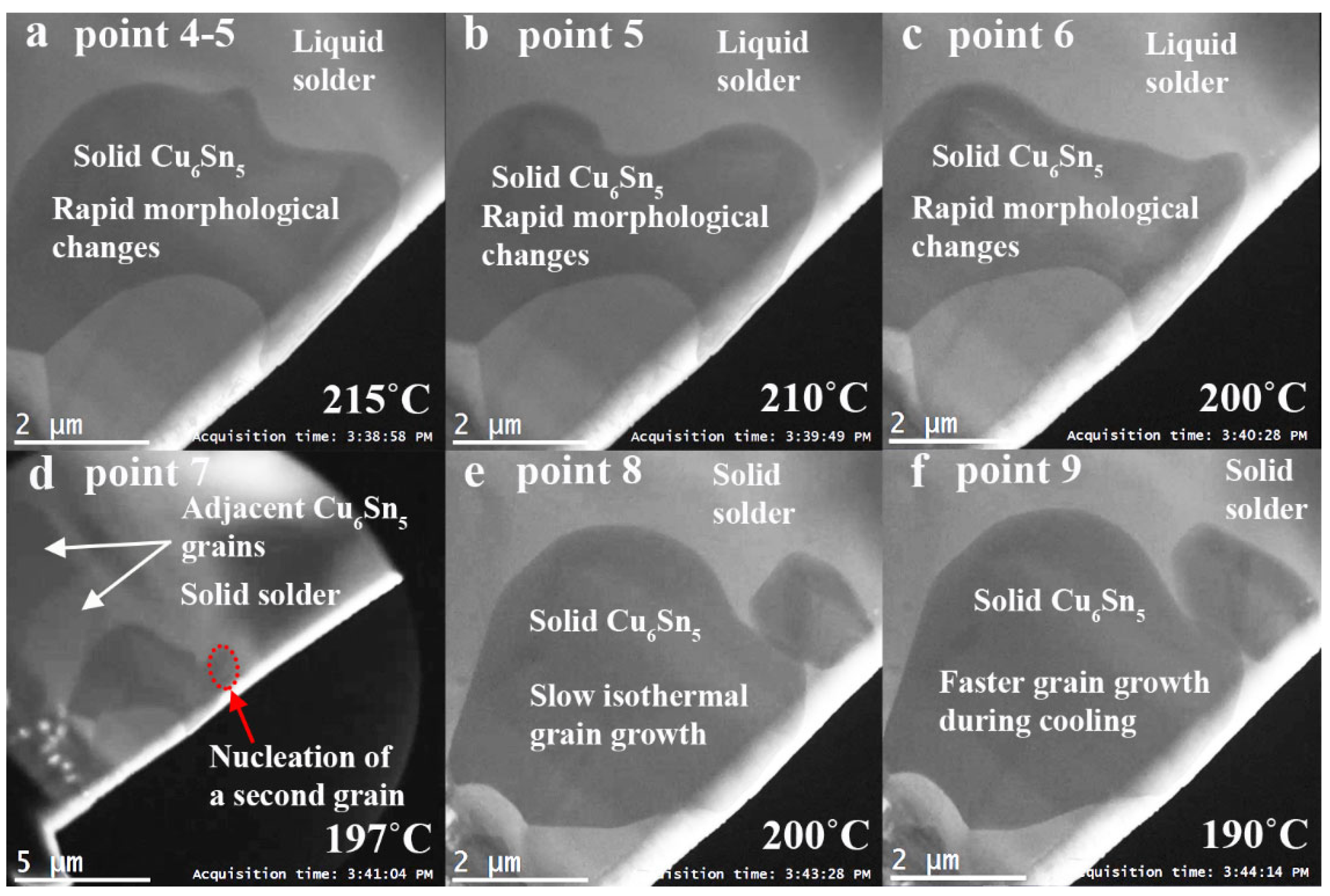
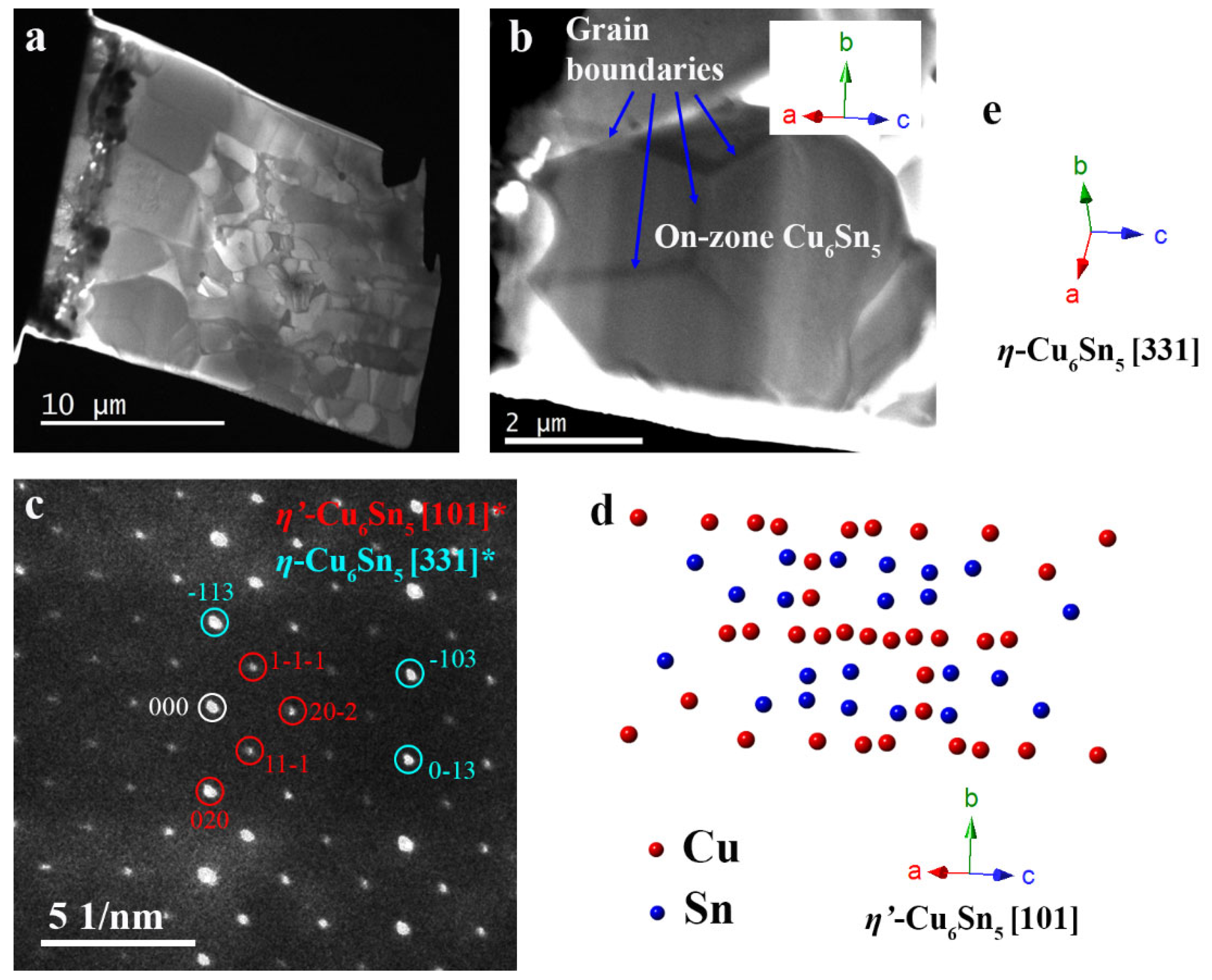
3. Results and Discussion

The SEM cross-section of the SAC305 solder ball reflow soldered on to the OSP Cu pad is shown in Figure 1a along with a higher magnification image displaying the Cu/IMCs/SAC interface. The Cu6Sn5 IMC has a scalloped-like morphology. Under BSE mode, the Sn-rich SAC305 solder matrix has a good contrast with the Cu6Sn5 IMC and the Cu substrate due to the differences in the averaged atomic numbers of approximately 50, 38.5 and 29, respectively. Ag has an atomic number of 47 which is relatively close to the atomic number of Sn, therefore the contrast between Ag3Sn and the Sn-rich matrix is low. The brighter spots in the Ag-LA EDS map in Figure 1b corresponds to the fine Ag3Sn plates, while the Sn-LA and Cu-KA maps help identify the Sn-rich SAC305 solder, the Cu6Sn5 IMC and the Cu substrate. The Cu3Sn IMC layer in the as reflowed joint was thin and was not visible due to the resolution limit of the SEM. The observed microstructure agrees with those widely reported in soldering literature [23,24].
Figure 2a,b show the TEM lamellar and an on-zone Cu6Sn5 grain, respectively. The Cu3Sn layer thickened as a result of ageing at 150 °C for 500 h [2,3,23]. Kirkendall voids, which often accompany the formation of Cu3Sn [3], are present between the Cu3Sn and the OSP-Cu (Figure 2a). The selected grain is not directly connected to the OSP-Cu/Cu3Sn, and the boundaries between the on-zone grain and four other Cu6Sn5 grains are outlined in Figure 2b. The selected area electron diffraction (SAED) pattern of this grain in Figure 2c is indexed to the [100] zone axis of η′-Cu6Sn5 (monoclinic, C2/c, International Centre for Diffraction Data, ICDD number: 047-1575) crystal structure, at the crystal orientation shown in Figure 2d. The Cu6Sn5 grain grew with the c-axis of the equivalent η-Cu6Sn5 crystal structure (hexagonal, P63/mmc, International Centre for Diffraction Data, ICDD number: 045-1488) perpendicular to the surface of the OSP-Cu, which is consistent with the preferred orientation reported in the literature [11].
Video S1 (Supplementary Materials) shows the recorded video during the heating experiment that is accelerated 20 times. Between point 1 and 2, the sample was heated to 120 °C at a rate of 61 °C/min. Between point 2 and 3, the heating rate was reduced to 32 °C/min to reduce temperature overshoot. It is expected that the Cu6Sn5 grains transform from a monoclinic η′ crystal structure to a η crystal structure around 186 °C [25] during this stage as observed in published TEM works [4,6]. During these heating stages, the selected Cu6Sn5 grain grew gradually (Figure 3a–c) until the temperature reached 211 °C at point 3, where rapid changes in the morphology of the solid Cu6Sn5 were observed (Figure 3c–i). Figure 3c–g are 1-s interval snapshots over a 4 s period highlighting the rapid grain boundary movements starting from point 3. It is believed that at this point the SAC305 solder (solidus at 217 °C) has started to melt while the Cu6Sn5 grain remained solid (solidus at 408 °C). The presence of liquid solder at this temperature is expected to enhance diffusion rates within the solder. The solidus is lower than the expected 217 °C, potentially due to electron beam heating. Since the metallic sample and the sample stage have good thermal conductivities, it is expected that the difference between the real sample temperature and the read-out temperature is small, though this may have also contributed to the sample melting at a lower read-out temperature. The sample appears to be self-sustaining despite the presence of liquid likely due to the mechanical strength imparted by the surface tension of the thin oxide film (581 mN m−1 at the melting point of Sn [26]), similar to the case in the Al-Si experiment conducted by Howe and Saka [12]. Furthermore, Sn has a vapor pressure at the order of 1 × 10⁻²⁰ Pa close to its melting point [27], that is orders of magnitude lower than the vapor pressure of Al alloys at the order of 7 × 10⁻⁹ Pa at the Al-Si eutectic of 577 °C [28] and is less likely to vaporize under the TEM vacuum. The dark contrast of the selected Cu6Sn5 grain is evidence that the grain remained solid throughout the heating experiment, as it continues to diffract the electron beam. The fast movement at the Cu6Sn5/SAC interface, measured up to 2.5 μm/s (movement of point P to point Q in Figure 3h,i), is due to the dissolution of the solid Cu6Sn5, as observed during a second reflow in an ex-situ experiment performed by Gong et al. [11]. On the other hand, at the bottom left of the grain, which is closer to the Cu3Sn layer, grain growth towards the direction of the Cu source was observed.
Sample heating was stopped shortly after point 3 after the rapid morphological changes were observed. The temperature overshot to 218 °C at point 4, before cooling to a set temperature of 210 °C at point 5 and then 200 °C at point 6, and was maintained at this near-isothermal temperature for 180 s. The rapid grain boundary movements continued through from point 3 to point 7 (Figure 3c–i and Figure 4a–c). A second Cu6Sn5 grain nucleated at point 7 (Figure 4d), where a minimum temperature at 197 °C was measured. In Figure 4d, the video is zoomed out to a lower magnification to provide a view of the area surrounding the selected Cu6Sn5 grain, where the grain boundaries of two adjacent grains are visible to the top-left of the selected grain. The morphological changes became sluggish from this point onwards (Figure 4d,e), as the SAC305 solder solidified. At this stage, the bottom left of the Cu6Sn5 grain has grown to less than 1 μm from the Cu3Sn. From point 8 to 9, the sample was cooled to 190 °C. During cooling, the growth rate of the two Cu6Sn5 grains accelerated (Figure 4e,f), as the dissolution limit of Cu in the SAC alloy reduced with temperature [11], and the excess Cu was deposited onto the Cu6Sn5 grains. Gong et al. [11] state that the heterogeneous dissolution and growth may have resulted in the scallop morphology of the Cu6Sn5 phase. The in situ observation in this study shows the Cu6Sn5 grain does not have a scallop morphology during dissolution, and the scallop morphology is formed when Cu is deposited onto the Cu6Sn5 grains during cooling.
The Gibbs–Thomson effect results in chemical potential variations across the curved interface between the solid Cu6Sn5 and liquid solder which can lead to undercooling [29,30]. The concentration of Cu in liquid solder at the localized surface of the grain, Cr, is given by [31]
C r   C 0   1 + 2 γ S L Ω r R T ,   when   2 γ S L Ω r R T 1 ,
where C0 is the concentration of Cu in the solder, γSL is the solid-liquid interfacial energy, Ω is the molar volume of Cu6Sn5, R is the gas constant, T is the temperature, and r is the radius of curvature which is positive for a convex grain interface and negative for a concave grain interface [32]. Therefore, a convex Cu6Sn5 interface of small curvature radius r, will increase the local concentration of Cu while a concave surface will result in a local Cu concentration that is lower than the Cu concentration in the solder. As a result, apart from the Cu fluxes from Cu3Sn and the adjacent Cu6Sn5 grains which promotes grain growth and Ostwald ripening [31,33], there is also Cu flux exchange at different local interfaces within a grain due to the difference in curvature radii, which may have contributed to the rapid changes in morphology at the Cu6Sn5/liquid interface. The Cu flux, J, can be calculated by the following equation [31],
J = D C r 1 C r 2 L = 2 γ S L Ω D C 0 L R T 1 r 1 1 r 2 ,
where D is the diffusivity of Cu in liquid solder, Cr1 and Cr2 are the Cu concentrations in liquid solder at two localized point surfaces calculated by Equation (1), L is the distance between the two points, and r1 and r2 are the radii of curvature at point 1 and point 2 respectively.
After the real-time observation, the sample was held at 190 °C for 30 min. Again, slow grain growth was observed during this period. This was followed by 9 min at 150 °C and 25 min at 120 °C before the sample was cooled to room temperature (Figure 5a,b). The sample was again tilted to a low index zone axis of the selected Cu6Sn5 grain and the SAED pattern was captured and indexed (Figure 5c). As indicated by the monoclinic reflections in Figure 5c, the grain has the crystal structure of a η′-Cu6Sn5, which is expected as the annealing stages allowed the high temperature η to fully convert into η′ as observed by Somidin et al. under HV-TEM [4,5]. The grain orientation is unchanged (Figure 5b,c), with the c-axis of an equivalent η-Cu6Sn5 crystal perpendicular to the OSP-Cu (Figure 5c,e). The low resolution plasmon filtered image of the sample in Figure 5a shows significant growth in all Cu6Sn5 grains in the direction perpendicular to the OSP-Cu. In contrast, no Cu6Sn5 grain coalescence was observed and there is no lateral growth.
After 30 min of annealing at 190 °C, part of the selected Cu6Sn5 grain has connected to the Cu3Sn phase. The growth in this direction continued during subsequent annealing at 150 °C and 120 °C, resulting in the final microstructure shown in Figure 5a,b. Again, the Ostwald ripening growth model [31,33] was not observed and there is no lateral growth during the annealing stages. Lord et al. [9] reported that lateral growth begins after the concentration of Cu in the solder reaches the dissolution limit. It is likely that the SAC305 in this experiment was not saturated due to the relatively short time above the melting temperature of the solder, which explains the lack of lateral growth.

4. Conclusions

The presented results are the first direct in situ observation of the dissolution of Cu6Sn5 at the solid Cu6Sn5/liquid solder interface and Cu6Sn5 growth at the Cu6Sn5/Cu3Sn interface at these temperatures. With this, the singular behavior of the solid/liquid interface with a weak surface tension is disclosed. That is, the phase boundary between Cu6Sn5 and SAC305 softened significantly when the latter is in a molten state, likely owing to repeated partial dissolution and re-solidification of Cu6Sn5 into and from SAC305.
The observation is consistent with published snapshots of the process based on ex-situ techniques in Gong et al.’s work, using a Sn-Ag-Cu alloy with slightly higher alloying contents i.e., Sn-3.8 wt%Ag-0.7 wt%Cu [11]. As long as the composition of the solder is below the solubility limits, Cu6Sn5 dissolves into the solder resulting in rapid changes in grain morphology above the solidus of the solder. Furthermore, the growth of Cu6Sn5 in the direction of Cu3Sn (Cu source) is substantial during soldering at high temperature; while the growth in the direction of the solder happens during cooling due to the deposition of Cu from the melt as the solubility of Cu reduces with decreasing temperature. This observation can help in designing strategies to reduce the thickness of the brittle Cu6Sn5 IMCs which are a primary failure point in solder joints and improve joint reliability, for example, by applying a temperature gradient to drive the diffusion of Cu away from the IMC/liquid interface and by replenishing the solder bath during wave soldering with solder alloys of lower Cu to maintain the Cu concentration in the melt.
This method for observing solid/liquid interaction using HV-TEM is likely to find application for other alloy/substrate systems such as those found in coating or welding processes to provide further understandings of the mechanisms involved. While the HV-TEM method allows for the use of thicker samples and edge-effects are less likely to influence the observed microstructural changes, further work is required to determine how closely these processes approach those occurring in bulk samples of industrially significant length scales.

Supplementary Materials

The following are available online at www.mdpi.com/article/10.3390/ma15020510/s1, Video S1: The recorded video accelerated 20 times.

Author Contributions

Conceptualization, K.N. and S.M.; methodology, F.S., K.N. and H.M.; validation, X.F.T., S.D.M. and M.J.B.; formal analysis, X.F.T., F.S. and K.N.; investigation, F.S., K.N. and H.M.; resources, K.N. and S.M.; writing—original draft preparation, X.F.T.; writing—review and editing, X.F.T., F.S., M.J.B., S.D.M., S.M. and K.N.; visualization, X.F.T. and F.S.; supervision, K.N.; project administration, K.N.; funding acquisition, K.N. and S.M. All authors have read and agreed to the published version of the manuscript.

Funding

This work was supported by the University of Queensland (UQ) [UQ-KU project], Nihon Superior [2016001895], the Australian Research Council [DP200101949], MEXT Japan [JPMXP09-A-17-KU-224], and Kyushu University [Progress 100 program].

Institutional Review Board Statement

Not applicable.

Informed Consent Statement

Not applicable.

Data Availability Statement

The data presented in this study are available on request from the corresponding author.

Acknowledgments

The authors acknowledge the facilities, and the scientific and technical assistance, of the Australian Microscopy & Microanalysis Research Facility at the Centre for Microscopy and Microanalysis, The University of Queensland, in particular for the access to the FIB SCIOS system for TEM sample preparation.

Conflicts of Interest

The authors declare no conflict of interest.

References

  1. Cheng, S.; Huang, C.-M.; Pecht, M. A review of lead-free solders for electronics applications. Microelectron. Reliab. 2017, 75, 77–95. [Google Scholar] [CrossRef]
  2. Mayappan, R.; Ghani, N.A.A.; Yahya, I. The effect of Ni addition on Cu-Sn intermetallic growth rate values in the SAC solder. AIP Conf. Proc. 2018, 2031, 020016. [Google Scholar] [CrossRef]
  3. Ng, W.C.W.; Sweatman, K.; Akaiwa, T.; Nishimura, T.; Sato, M.; Gourlay, C.; Belyakov, S. Dissolution in service of the copper substrate of solder joints. In Proceedings of the 2016 IEEE 18th Electronics Packaging Technology Conference (EPTC), Singapore, 30 November–3 December 2016. [Google Scholar]
  4. Somidin, F.; Maeno, H.; Mohd Salleh, M.A.A.; Tran, X.Q.; McDonald, S.D.; Matsumura, S.; Nogita, K. Characterising the polymorphic phase transformation at a localised point on a Cu6Sn5 grain. Mater. Charact. 2018, 138, 113–119. [Google Scholar] [CrossRef]
  5. Somidin, F.; Maeno, H.; Tran, X.Q.; McDonald, S.D.; Mohd Salleh, M.A.A.; Matsumura, S.; Nogita, K. Imaging the Polymorphic Transformation in a Single Cu6Sn5 Grain in a Solder Joint. Materials 2018, 11, 2229. [Google Scholar] [CrossRef] [PubMed] [Green Version]
  6. Somidin, F.; Maeno, H.; Toriyama, T.; McDonald, S.D.; Yang, W.; Matsumura, S.; Nogita, K. Direct observation of the Ni stabilising effect in interfacial (Cu,Ni)6Sn5 intermetallic compounds. Materialia 2020, 9, 100530. [Google Scholar] [CrossRef]
  7. Mohd Salleh, M.A.A.; McDonald, S.D.; Yasuda, H.; Sugiyama, A.; Nogita, K. Rapid Cu6Sn5 growth at liquid Sn/solid Cu interfaces. Scr. Mater. 2015, 100, 17–20. [Google Scholar] [CrossRef]
  8. Mohd Salleh, M.A.A.; Gourlay, C.M.; Xian, J.W.; Belyakov, S.A.; Yasuda, H.; McDonald, S.D.; Nogita, K. In situ imaging of microstructure formation in electronic interconnections. Sci. Rep. 2017, 7, 40010. [Google Scholar] [CrossRef] [Green Version]
  9. Lord, R.A.; Umantsev, A. Early stages of soldering reactions. J. Appl. Phys. 2005, 98, 063525. [Google Scholar] [CrossRef] [Green Version]
  10. Pan, C.-C.; Yu, C.-H.; Lin, K.-L. The amorphous origin and the nucleation of intermetallic compounds formed at the interface during the soldering of Sn–3.0Ag–0.5Cu on a Cu substrate. Appl. Phys. Lett. 2008, 93, 061912. [Google Scholar] [CrossRef]
  11. Gong, J.; Liu, C.; Conway, P.P.; Silberschmidt, V.V. Evolution of CuSn intermetallics between molten SnAgCu solder and Cu substrate. Acta Mater. 2008, 56, 4291–4297. [Google Scholar] [CrossRef]
  12. Howe, J.M.; Saka, H. In Situ Transmission Electron Microscopy Studies of the Solid–Liquid Interface. MRS Bull. 2011, 29, 951–957. [Google Scholar] [CrossRef]
  13. Matsuki, H.; Ibuka, H.; Saka, H. TEM observation of interfaces in a solder joint in a semiconductor device. Sci. Technol. Adv. Mater. 2002, 3, 261–270. [Google Scholar] [CrossRef]
  14. Saka, H.; Sasaki, K.; Tsukimoto, S.; Arai, S. In situ Observation of Solid–liquid Interfaces by Transmission Electron Microscopy. J. Mater. Res. 2005, 20, 1629–1640. [Google Scholar] [CrossRef]
  15. Torazawa, N.; Arai, S.; Takase, Y.; Sasaki, K.; Saka, H. Transmission Electron Microscopy of Interfaces in Joints between Pb-Free Solders and Electroless Ni-P. Mater. Trans. 2003, 44, 1438–1447. [Google Scholar] [CrossRef]
  16. Lee, J.G.; Mori, H. In-situobservation of alloy phase formation in nanometre-sized particles in the Sn–Bi system. Philos. Mag. 2004, 84, 2675–2686. [Google Scholar] [CrossRef]
  17. Lee, J.G.; Mori, H.; Yasuda, H. In situobservation of a fluid amorphous phase formed in isolated nanometer-sized particles in the Sn-Bi system. Phys. Rev. B 2002, 66, 012105. [Google Scholar] [CrossRef]
  18. Allen, G.L.; Bayles, R.A.; Gile, W.W.; Jesser, W.A. Small particle melting of pure metals. Thin Solid Film. 1986, 144, 297–308. [Google Scholar] [CrossRef]
  19. Lai, S.L.; Guo, J.Y.; Petrova, V.V.; Ramanath, G.; Allen, L.H. Size-Dependent Melting Properties of Small Tin Particles: Nanocalorimetric Measurements. Phys. Rev. Lett. 1996, 77, 99–102. [Google Scholar] [CrossRef] [PubMed] [Green Version]
  20. Tan, X.F.; Yang, W.; Aso, K.; Matsumura, S.; McDonald, S.D.; Nogita, K. Evidence of Copper Separation in Lithiated Cu6Sn5 Lithium-Ion Battery Anodes. ACS Appl. Energy Mater. 2019, 3, 141–145. [Google Scholar] [CrossRef] [Green Version]
  21. Sadamatsu, S.; Tanaka, M.; Higashida, K.; Matsumura, S. Transmission electron microscopy of bulk specimens over 10microm in thickness. Ultramicroscopy 2016, 162, 10–16. [Google Scholar] [CrossRef] [PubMed] [Green Version]
  22. Omoto, K.; Tsuno, K.; Ohsaki, M.; Matsumura, S.; Tomokiyo, Y. Omega filter installed in the 1MV microscope of Kyushu University. Micron 2008, 39, 666–675. [Google Scholar] [CrossRef]
  23. Zhang, X.; Hu, X.; Jiang, X.; Li, Y. Effect of Ni addition to the Cu substrate on the interfacial reaction and IMC growth with Sn3.0Ag0.5Cu solder. Appl. Phys. A 2018, 124, 315. [Google Scholar] [CrossRef]
  24. Li, S.; Liu, Y.; Zhang, H.; Cai, H.; Sun, F.; Zhang, G. Microstructure and hardness of SAC305 and SAC305-0.3Ni solder on Cu, high temperature treated Cu, and graphene-coated Cu substrates. Results Phys. 2018, 11, 617–622. [Google Scholar] [CrossRef]
  25. Zeng, G.; McDonald, S.D.; Read, J.J.; Gu, Q.; Nogita, K. Kinetics of the polymorphic phase transformation of Cu6Sn5. Acta Mater. 2014, 69, 135–148. [Google Scholar] [CrossRef]
  26. Passerone, A.; Ricci, E.; Sangiorgi, R. Influence of oxygen contamination on the surface tension of liquid tin. J. Mater. Sci. 1990, 25, 4266–4272. [Google Scholar] [CrossRef]
  27. Lide, D.R. CRC Handbook of Chemistry and Physics, 87th ed Editor-in-Chief:  David R. Lide (National Institute of Standards and Technology). CRC Press/Taylor and Francis Group:  Boca Raton, FL. 2006. 2608 pp. $139.95. ISBN 0-8493-0487-3. J. Am. Chem. Soc. 2006, 129, 724. [Google Scholar] [CrossRef]
  28. Jeong, J.; Lee, S.; Jeon, J.-B.; Kim, S. Excessively High Vapor Pressure of Al-based Amorphous Alloys. Metals 2015, 5, 1878–1886. [Google Scholar] [CrossRef] [Green Version]
  29. Xian, J.W.; Belyakov, S.A.; Ivier, M.; Nogita, K.; Yasuda, H.; Gourlay, C.M. Cu6Sn5 crystal growth mechanisms during solidification of electronic interconnections. Acta Mater. 2017, 126, 540–551. [Google Scholar] [CrossRef]
  30. Nakano, K.; Narumi, T.; Morishita, K.; Yasuda, H. Characterization of Growing Dendrites in CrMnFeCoNi High-Entropy Alloy by Time-Resolved and In-Situ Tomography. Mater. Trans. 2020, 61, 596–604. [Google Scholar] [CrossRef] [Green Version]
  31. Kim, H.K.; Tu, K.N. Kinetic analysis of the soldering reaction between eutectic SnPb alloy and Cu accompanied by ripening. Phys. Rev. B Condens. Matter. 1996, 53, 16027–16034. [Google Scholar] [CrossRef]
  32. Gusak, A.M.; Tu, K.N.; Chen, C. Extremely rapid grain growth in scallop-type Cu6Sn5 during solid–liquid interdiffusion reactions in micro-bump solder joints. Scr. Mater. 2020, 179, 45–48. [Google Scholar] [CrossRef]
  33. Kim, H.K.; Liou, H.K.; Tu, K.N. Three-dimensional morphology of a very rough interface formed in the soldering reaction between eutectic SnPb and Cu. Appl. Phys. Lett. 1995, 66, 2337–2339. [Google Scholar] [CrossRef]
Figure 1. (a) SEM cross-section of the as reflowed Cu/IMCs/SAC solder joint at two different magnifications. (b) Sn, Cu and Ag EDS maps of the Cu/IMCs/SAC solder joint. (c) Temperature profile of the heating experiment, showing different time intervals (points 1–9) through the heating cycle.
Materials 15 00510 g001
Figure 2. (a) Low magnification on-zone bright-field (BF) plasmon filtered TEM image of the lamellar before the heating experiment. (b) Image of the on-zone Cu6Sn5 on top of four other Cu6Sn5 grains, and (c) the SAED pattern of the on-zone grain (d) a schematic of the crystal structure showing the crystal orientation, and (e) the equivalent orientation in a η-Cu6Sn5 crystal to produce the diffraction pattern indexed in (c).
Materials 15 00510 g002
Figure 3. Snapshots of the heating experiment at each of the time intervals indicated in Figure 1c: (a) point 1, (b) point 2, (cg) 1-s interval snapshots over a 4 s period highlighting the rapid grain boundary movements starting from point 3, (h) between point 3 and 4 at 215 °C and (i) point 4.
Materials 15 00510 g003
Figure 4. Snapshots of the heating experiment (a) between point 4 and 5, (b) at point 5, (c) point 6, (d) point 7 (zoomed out to provide a view of the area surrounding the selected grain), (e) point 8 and (f) point 9.
Materials 15 00510 g004
Figure 5. (a) Low magnification image of the lamellar after the heating experiment, (b) image of the on-zone Cu6Sn5 grain after tilting, (c) the SAED pattern and (d) a schematic of the crystal structure of the on-zone η′-Cu6Sn5 grain showing the grain orientation, and (e) the equivalent orientation in a η-Cu6Sn5 crystal to produce the diffraction pattern indexed in (c).
Materials 15 00510 g005
Publisher’s Note: MDPI stays neutral with regard to jurisdictional claims in published maps and institutional affiliations.

