
Resistive Switching Characteristics of Alloyed AlSiOx Insulator for Neuromorphic Devices

Abstract
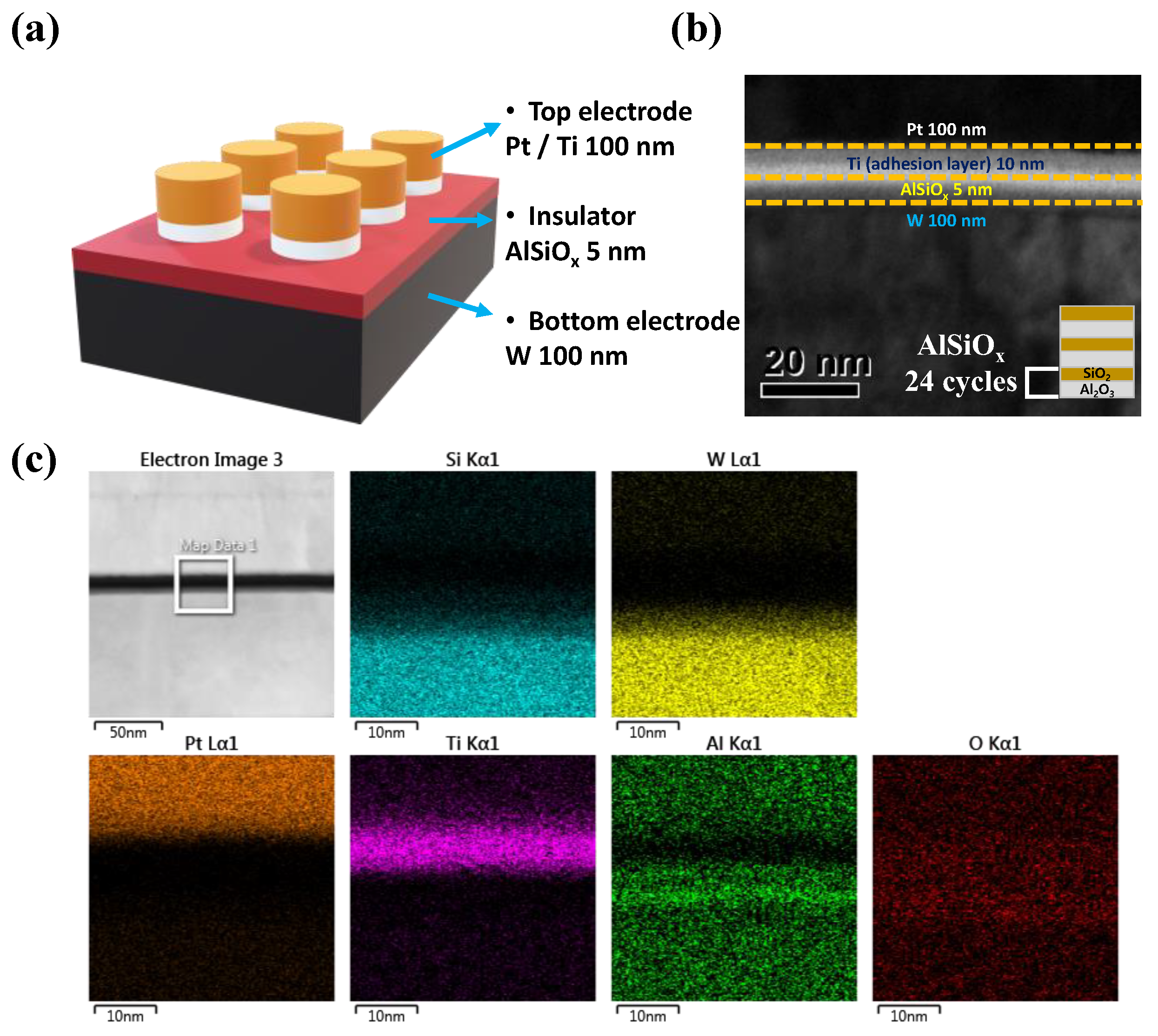
:1. Introduction
2. Experiments
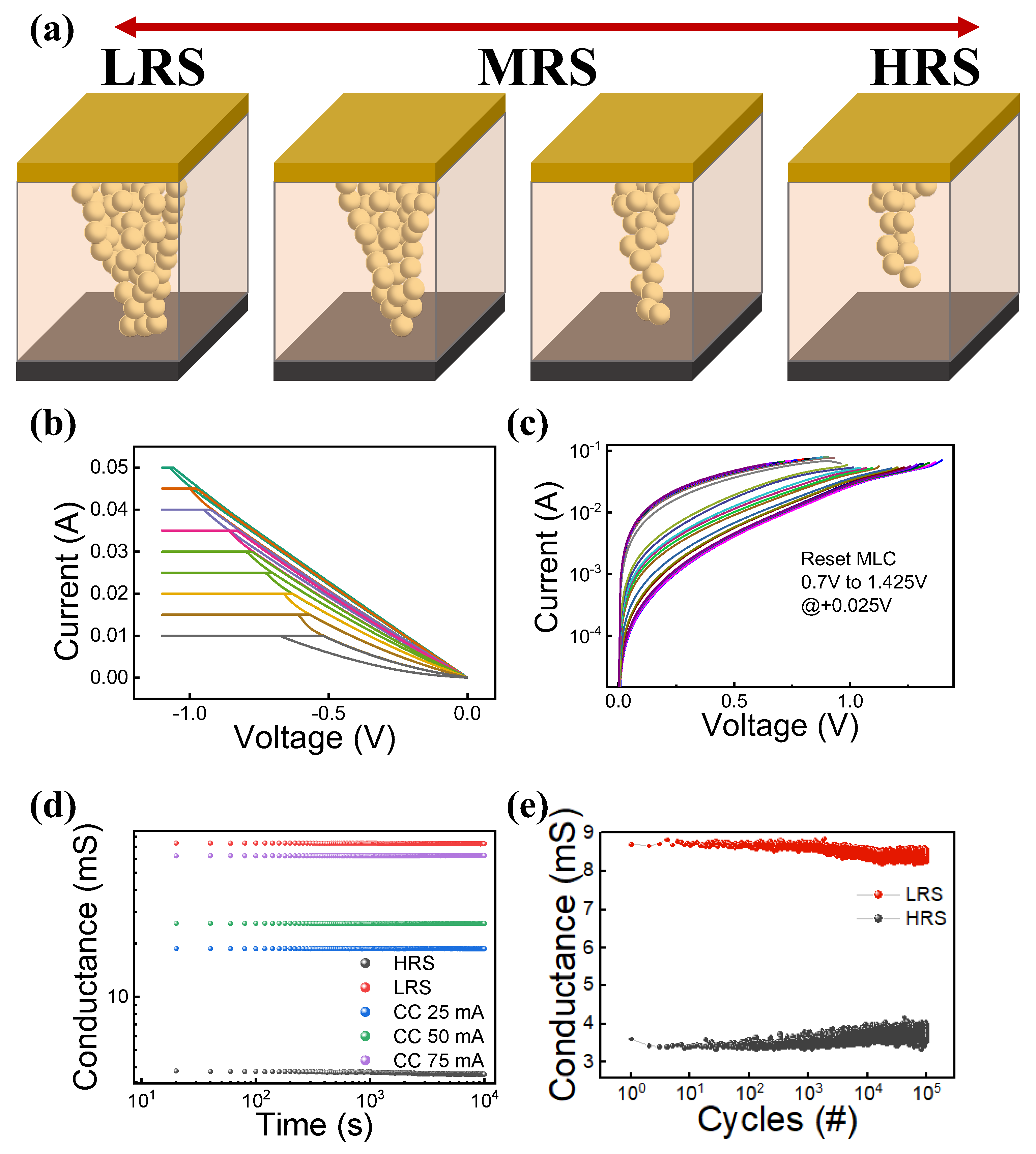
3. Results and Discussions
4. Conclusions
Author Contributions
Funding
Data Availability Statement
Conflicts of Interest
References
- Park, M.; Kang, M.; Kim, S. Pulse Frequency Dependent Synaptic Characteristics in Ta/SiN/Si Memristor Device for Neuromorphic System. J. Alloys Compd. 2021, 882, 160760. [Google Scholar] [CrossRef]
- Ismail, M.; Mahata, C.; Kwon, O.; Kim, S. Neuromorphic Synapses with High Switching Uniformity and Multilevel Memory Storage Enabled through a Hf-Al-O Alloy for Artificial Intelligence. ACS Appl. Electron. Mater. 2022, 4, 1288–1300. [Google Scholar] [CrossRef]
- Ryu, J.H.; Mahata, C.; Kim, S. Long-Term and Short-Term Plasticity of Ta2O5/HfO2 Memristor for Hardware Neuromorphic Application. J. Alloys Compd. 2021, 850, 156675. [Google Scholar] [CrossRef]
- Lu, K.; Li, Y.; He, W.F.; Chen, J.; Zhou, Y.X.; Duan, N.; Jin, M.M.; Gu, W.; Xue, K.H.; Sun, H.J.; et al. Diverse Spike-Timing-Dependent Plasticity Based on Multilevel HfOx Memristor for Neuromorphic Computing. Appl. Phys. A Mater. Sci. Process. 2018, 124, 438. [Google Scholar] [CrossRef]
- Kim, S.; Kim, H.; Hwang, S.; Kim, M.H.; Chang, Y.F.; Park, B.G. Analog Synaptic Behavior of a Silicon Nitride Memristor. ACS Appl. Mater. Interfaces 2017, 9, 40420–40427. [Google Scholar] [CrossRef] [PubMed]
- Waser, R.; Aono, M. Nanoionics-Based Resistive Switching Memories. Nat. Mater. 2007, 6, 833–840. [Google Scholar] [CrossRef] [PubMed]
- Sawa, A. Resistive Switching in Transition Metal Oxides. Mater. Today 2008, 11, 28–36. [Google Scholar] [CrossRef]
- Yu, S. Overview of Resistive Switching Memory (RRAM) Switching Mechanism and Device Modeling. In Proceedings of the Proceedings—IEEE International Symposium on Circuits and Systems, Melbourne, VIC, Australia, 1–5 June 2014. [Google Scholar]
- Li, Y.T.; Long, S.B.; Liu, Q.; Lü, H.B.; Liu, S.; Liu, M. An Overview of Resistive Random Access Memory Devices. Chin. Sci. Bull. 2011, 56, 3072–3078. [Google Scholar] [CrossRef] [Green Version]
- Kim, D.; Kim, S.; Kim, S. Logic-in-Memory Application of CMOS Compatible Silicon Nitride Memristor. Chaos Solitons Fractals 2021, 153, 111540. [Google Scholar] [CrossRef]
- Lin, K.L.; Hou, T.H.; Shieh, J.; Lin, J.H.; Chou, C.T.; Lee, Y.J. Electrode Dependence of Filament Formation in HfO2 Resistive-Switching Memory. J. Appl. Phys. 2011, 109, 084104. [Google Scholar] [CrossRef]
- Rodriguez-Fernandez, A.; Aldana, S.; Campabadal, F.; Sune, J.; Miranda, E.; Jimenez-Molinos, F.; Roldan, J.B.; Gonzalez, M.B. Resistive Switching with Self-Rectifying Tunability and Influence of the Oxide Layer Thickness in Ni/HfO2/N+-Si RRAM Devices. IEEE Trans. Electron. Devices 2017, 64, 3159–3166. [Google Scholar] [CrossRef]
- Hu, G.; An, H.; Xi, J.; Lu, J.; Hua, Q.; Peng, Z. A ZnO Micro/Nanowire-Based Photonic Synapse with Piezo-Phototronic Modulation. Nano Energy 2021, 89, 106282. [Google Scholar] [CrossRef]
- Khan, S.A.; Lee, G.H.; Mahata, C.; Ismail, M.; Kim, H.; Kim, S. Bipolar and Complementary Resistive Switching Characteristics and Neuromorphic System Simulation in a Pt/ZnO/TiN Synaptic Device. Nanomaterials 2021, 11, 315. [Google Scholar] [CrossRef]
- Shin, J.; Kang, M.; Kim, S. Gradual Conductance Modulation of Ti/WOx/Pt Memristor with Self-Rectification for a Neuromorphic System. Appl. Phys. Lett. 2021, 119, 012102. [Google Scholar] [CrossRef]
- Sun, J.; Tan, J.B.; Chen, T. Investigation of Electrical Noise Signal Triggered Resistive Switching and Its Implications. IEEE Trans. Electron. Devices 2020, 67, 4178–4184. [Google Scholar] [CrossRef]
- Science, A.M. Comparative Study of Atomic-Layer-Deposited Stacked (HfO2/Al2O3) and Nanolaminated (HfAlOx) Dielectrics on In0.53Ga0.47As. ACS Appl. Mater. Interfaces 2012, 5, 4195–4201. [Google Scholar]
- Lu, B.; Lv, H.; Zhang, Y.; Zhang, Y.; Liu, C. Comparison of HfAlO, HfO2/Al2O3, and HfO2 on n-Type GaAs Using Atomic Layer Deposition. Superlattices Microstruct. 2016, 99, 54–57. [Google Scholar] [CrossRef]
- Komatsu, N.; Tanaka, H.; Aoki, H.; Masumoto, K.; Honjo, M.; Kimura, C.; Okumura, Y.; Sugino, T. Effect of Nitrogen Doping on the Properties of AlSiO Film for Wide Bandgap Semiconductors. Appl. Surf. Sci. 2010, 257, 1437–1440. [Google Scholar] [CrossRef]
- Komatsu, N.; Masumoto, K.; Aoki, H.; Kimura, C.; Sugino, T. Characterization of Si-Added Aluminum Oxide (AlSiO) Films for Power Devices. Appl. Surf. Sci. 2010, 256, 1803–1806. [Google Scholar] [CrossRef]
- Hong, X.L.; Loy, D.J.J.; Dananjaya, P.A.; Tan, F.; Ng, C.M.; Lew, W.S. Oxide-Based RRAM Materials for Neuromorphic Computing. J. Mater. Sci. 2018, 53, 8720–8746. [Google Scholar] [CrossRef]
- Chen, H.Y.; Brivio, S.; Chang, C.C.; Frascaroli, J.; Hou, T.H.; Hudec, B.; Liu, M.; Lv, H.; Molas, G.; Sohn, J.; et al. Resistive Random Access Memory (RRAM) Technology: From Material, Device, Selector, 3D Integration to Bottom-up Fabrication. J. Electroceram. 2017, 39, 21–38. [Google Scholar] [CrossRef]
- Mahata, C.; Algadi, H.; Ismail, M.; Kwon, D.; Kim, S. Controlled Multilevel Switching and Artificial Synapse Characteristics in Transparent HfAlO-Alloy Based Memristor with Embedded TaN Nanoparticles. J. Mater. Sci. Technol. 2021, 95, 203–212. [Google Scholar] [CrossRef]
- Mahata, C.; Kim, S. Modified Resistive Switching Performance by Increasing Al Concentration in HfO2 on Transparent Indium Tin Oxide Electrode. Ceram. Int. 2021, 47, 1199–1207. [Google Scholar] [CrossRef]
- Kim, B.; Mahata, C.; Ryu, H.; Ismail, M.; Yang, B.-D.; Kim, S. Alloyed High-k-Based Resistive Switching Memory in Contact Hole Structures. Coatings 2021, 11, 451. [Google Scholar] [CrossRef]
- Zhang, Y.; Duan, Z.; Li, R.; Ku, C.J.; Reyes, P.; Ashrafi, A.; Lu, Y. FeZnO-Based Resistive Switching Devices. J. Electron. Mater. 2012, 41, 2880–2885. [Google Scholar] [CrossRef]
- Ryu, H.; Choi, J.; Kim, S. Voltage Amplitude-Controlled Synaptic Plasticity from Complementary Resistive Switching in Alloying HfOx with AlOx-Based RRAM. Metals 2020, 10, 1410. [Google Scholar] [CrossRef]
- Yang, M.Y.; Kamiya, K.; Magyari-Kope, B.; Momida, H.; Ohno, T.; Niwa, M.; Nishi, Y.; Shiraishi, K. Physical Guiding Principles for High Quality Resistive Random Access Memory Stack with Al2O3 Insertion Layer. Jpn. J. Appl. Phys. 2013, 52, 04CD11. [Google Scholar] [CrossRef]
- Chen, L.; Dai, Y.W.; Sun, Q.Q.; Guo, J.J.; Zhou, P.; Zhang, D.W. Al2O3/HfO2 Functional Stack Films Based Resistive Switching Memories with Controlled SET and RESET Voltages. Solid State Ion. 2015, 273, 66–69. [Google Scholar] [CrossRef]
- Degraeve, R.; Fantini, A.; Raghavan, N.; Goux, L.; Clima, S.; Govoreanu, B.; Belmonte, A.; Linten, D.; Jurczak, M. Causes and Consequences of the Stochastic Aspect of Filamentary RRAM. Microelectron. Eng. 2015, 147, 171–175. [Google Scholar] [CrossRef]
- Zahoor, F.; Azni Zulkifli, T.Z.; Khanday, F.A. Resistive Random Access Memory (RRAM): An Overview of Materials, Switching Mechanism, Performance, Multilevel Cell (Mlc) Storage, Modeling, and Applications. Nanoscale Res. Lett. 2020, 15, 1–26. [Google Scholar] [CrossRef]
- Lian, X.; Wang, M.; Rao, M.; Yan, P.; Yang, J.J.; Miao, F. Characteristics and transport mechanisms of triple switching regimes of TaOx memristor. Appl. Phys. Lett. 2017, 110, 173504. [Google Scholar] [CrossRef]
- Kim, S.; Jung, S.; Kim, M.-H.; Chen, Y.-C.; Chang, Y.-F.; Ryoo, K.-C.; Cho, S.; Lee, J.-H.; Park, B.-G. Scaling effect on silicon nitride memristor with highly doped Si substrate. Small 2018, 14, 1704062. [Google Scholar] [CrossRef] [PubMed]
- Cho, H.; Kim, S. Emulation of Biological Synapse Characteristics from Cu/Aln/Tin Conductive Bridge Random Access Memory. Nanomaterials 2020, 10, 1709. [Google Scholar] [CrossRef]
- Ismail, M.; Mahata, C.; Kim, S. Electronic Synaptic Plasticity and Analog Switching Characteristics in Pt/TiOx/AlOx/AlTaON/TaN Multilayer RRAM for Artificial Synapses. Appl. Surf. Sci. 2022, 599, 153906. [Google Scholar] [CrossRef]
- Park, J.; Lee, S.; Lee, K.; Kim, S. Conductance Quantization Behavior in Pt/Sin/Tan Rram Device for Multilevel Cell. Metals 2021, 11, 1918. [Google Scholar] [CrossRef]
- Kim, W.; Park, S., II; Zhang, Z.; Wong, S. Current Conduction Mechanism of Nitrogen-Doped AlOx RRAM. IEEE Trans. Electron Devices 2014, 61, 2158–2163. [Google Scholar] [CrossRef]
- Ismail, M.; Abbas, H.; Choi, C.; Kim, S. Stabilized and RESET-Voltage Controlled Multi-Level Switching Characteristics in ZrO2-Based Memristors by Inserting a-ZTO Interface Layer. J. Alloys Compd. 2020, 835, 155256. [Google Scholar] [CrossRef]
- Ismail, M.; Mahata, C.; Kim, S. Forming-Free Pt/Al2O3/HfO2/HfAlOx/TiN Memristor with Controllable Multilevel Resistive Switching and Neuromorphic Characteristics for Artificial Synapse. J. Alloys Compd. 2022, 892, 162141. [Google Scholar] [CrossRef]
- Lin, J.; Wang, S.; Liu, H. Multi-Level Switching of Al-Doped HfO2 RRAM with a Single Voltage Amplitude Set Pulse. Electronics 2021, 10, 731. [Google Scholar] [CrossRef]
- Wu, J.; Ye, C.; Zhang, J.; Deng, T.; He, P.; Wang, H. Multilevel Characteristics for Bipolar Resistive Random Access Memory Based on Hafnium Doped SiO2 Switching Layer. Mater. Sci. Semicond. Process. 2016, 43, 144–148. [Google Scholar] [CrossRef]
- Lee, Y.; Park, J.; Chung, D.; Lee, K.; Kim, S. Multi-Level Cells and Quantized Conductance Characteristics of Al2O3-Based RRAM Device for Neuromorphic System. Nanoscale Res. Lett. 2022, 17, 84. [Google Scholar] [CrossRef] [PubMed]
- Bliss, T.V.P.; Cooke, S.F. Long-Term Potentiation and Long-Term Depression: A Clinical Perspective. Clinics 2011, 66, 3–17. [Google Scholar] [CrossRef] [PubMed] [Green Version]
- Kim, S.G.; Han, J.S.; Kim, H.; Kim, S.Y.; Jang, H.W. Recent Advances in Memristive Materials for Artificial Synapses. Adv. Mater. Technol. 2018, 3, 1800457. [Google Scholar] [CrossRef] [Green Version]
- Park, J.; Ryu, H.; Kim, S. Nonideal Resistive and Synaptic Characteristics in Ag/ZnO/TiN Device for Neuromorphic System. Sci. Rep. 2021, 11, 16601. [Google Scholar] [CrossRef]
- Cho, H.; Kim, S. Enhancing Short-Term Plasticity by Inserting a Thin TiO2 Layer in WOx-Based Resistive Switching Memory. Coatings 2020, 10, 908. [Google Scholar] [CrossRef]
- Woo, J.; Moon, K.; Song, J.; Lee, S.; Kwak, M.; Park, J.; Hwang, H. Improved Synaptic Behavior under Identical Pulses Using AlOx/HfO2 Bilayer RRAM Array for Neuromorphic Systems. IEEE Electron. Device Lett. 2016, 37, 994–997. [Google Scholar] [CrossRef]


| Device Structure | Set Voltage (V) | Reset Voltage (V) | Current Level | On–Off Ratio | Retention (s) | MLC | Synaptic Characteristics |
|---|---|---|---|---|---|---|---|
| ITO/HfAlO/TaN–NP/HfAlO/ITO | −0.7 | 1 | 10 μA–1 mA | >10 | >104 | O | O |
| TiN/Ti/HfAlO/ITO | −0.5 | 0.75 | 10 μA–100 μA | >10 | >104 | O | O |
| Au/Ti/HfTiOx/p-Si | 6 | −2.5 | 1 nA–100 μA | >104 | >104 | - | O |
| Pt/HfAlOx/TiN | −1.5 | 1.5 | 10 μA–100 μA | >10 | - | O | O |
| Ag/FeZnO/Pt | 0.75 | −1 | 10 μA–10 mA | >3.8 × 10² | >107 | - | - |
| Ag/FeZnO/MgO/Pt | 1.5 | −1 | 10 nA–10 mA | >9.9 × 10⁵ | >107 | - | - |
| Pt/Ti/AlSiOx/W | −0.8 | 1.2 | 100 μA–5 mA | >10 | >104 | O | O |
Publisher’s Note: MDPI stays neutral with regard to jurisdictional claims in published maps and institutional affiliations. |
© 2022 by the authors. Licensee MDPI, Basel, Switzerland. This article is an open access article distributed under the terms and conditions of the Creative Commons Attribution (CC BY) license (https://creativecommons.org/licenses/by/4.0/).
Share and Cite
Lee, Y.; Jang, J.; Jeon, B.; Lee, K.; Chung, D.; Kim, S. Resistive Switching Characteristics of Alloyed AlSiOx Insulator for Neuromorphic Devices. Materials 2022, 15, 7520. https://doi.org/10.3390/ma15217520
Lee Y, Jang J, Jeon B, Lee K, Chung D, Kim S. Resistive Switching Characteristics of Alloyed AlSiOx Insulator for Neuromorphic Devices. Materials. 2022; 15(21):7520. https://doi.org/10.3390/ma15217520
Chicago/Turabian StyleLee, Yunseok, Jiung Jang, Beomki Jeon, Kisong Lee, Daewon Chung, and Sungjun Kim. 2022. "Resistive Switching Characteristics of Alloyed AlSiOx Insulator for Neuromorphic Devices" Materials 15, no. 21: 7520. https://doi.org/10.3390/ma15217520