

Fabrication of Ga2O3 Schottky Barrier Diode and Heterojunction Diode by MOCVD

 ,
, 
Abstract
:1. Introduction
2. Materials and Methods
3. Results
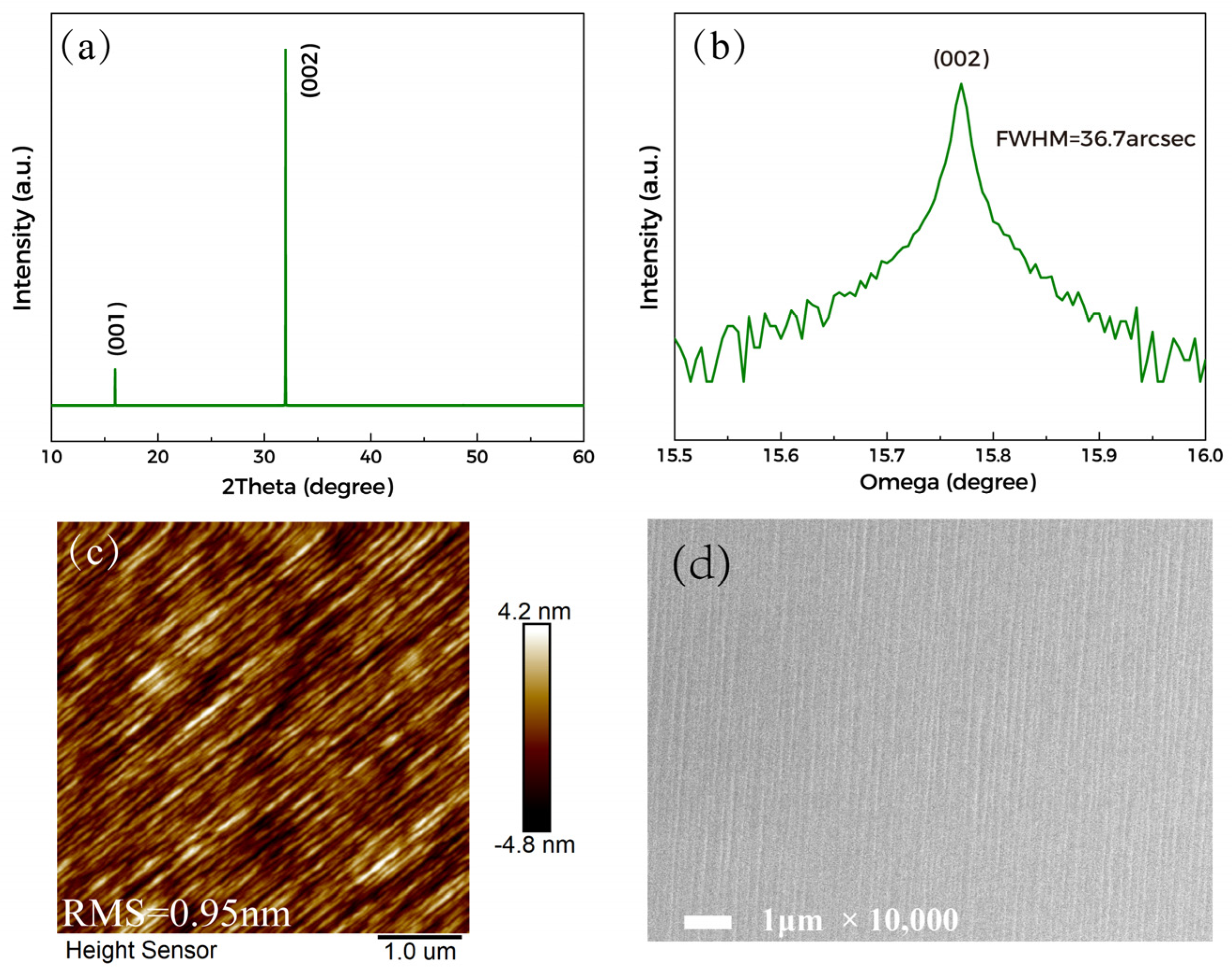
3.1. Film Characterization
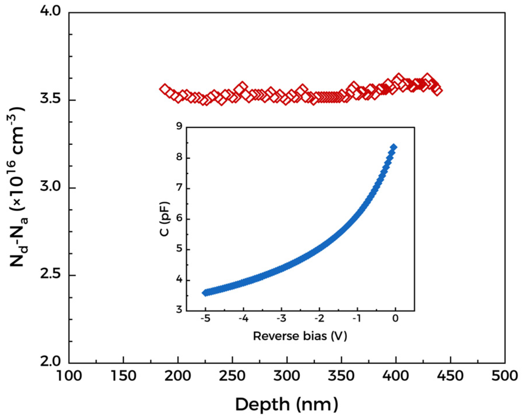
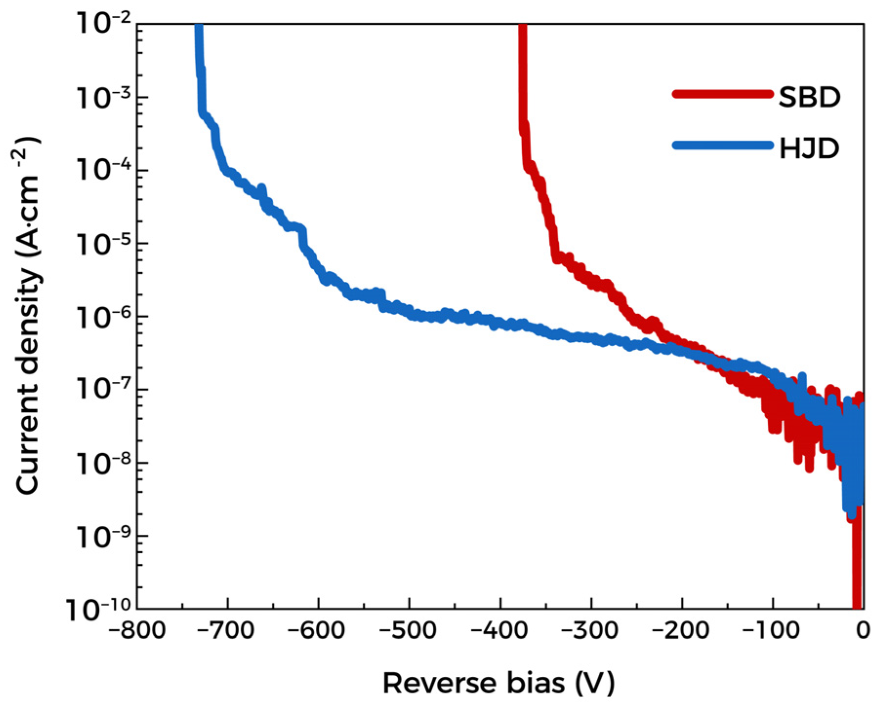
3.2. Devices Measurement
4. Discussion
5. Conclusions
Author Contributions
Funding
Institutional Review Board Statement
Informed Consent Statement
Data Availability Statement
Conflicts of Interest
References
- Pearton, S.J.; Yang, J.C.; Cary, P.H.; Ren, F.; Kim, J.; Tadjer, M.J.; Mastro, M.A. A review of Ga2O3 materials, processing, and devices. Appl. Phys. Rev. 2018, 5, 011301. [Google Scholar] [CrossRef] [Green Version]
- Zhang, J.Y.; Shi, J.L.; Qi, D.C.; Chen, L.; Zhang, K.H.L. Recent progress on the electronic structure, defect, and doping properties of Ga2O3. APL Mater. 2020, 8, 020906. [Google Scholar] [CrossRef] [Green Version]
- Higashiwaki, M.; Murakami, H.; Kumagai, Y.; Kuramata, A. Current status of Ga2O3 power devices. Jpn. J. Appl. Phys. 2016, 55, 1202A1. [Google Scholar] [CrossRef]
- Konishi, K.; Goto, K.; Murakami, H.; Kumagai, Y.; Kuramata, A.; Yamakoshi, S.; Higashiwaki, M. 1-kV vertical Ga2O3 field-plated Schottky barrier diodes. Appl. Phys. Lett. 2017, 110, 103506. [Google Scholar] [CrossRef]
- Wang, Y.G.; Cai, S.J.; Liu, M.; Lv, Y.J.; Long, S.B.; Zhou, X.Y.; Song, X.B.; Liang, S.X.; Han, T.T.; Tan, X.; et al. High-voltage (-201) beta-Ga2O3 vertical schottky barrier diode with thermally-oxidized termination. IEEE Electr. Device L. 2020, 41, 131–134. [Google Scholar] [CrossRef]
- Hoshikawa, K.; Ohba, E.; Kobayashi, T.; Yanagisawa, J.; Miyagawa, C.; Nakamura, Y. Growth of beta-Ga2O3 single crystals using vertical Bridgman method in ambient air. J. Cryst. Growth 2016, 447, 36–41. [Google Scholar] [CrossRef]
- Maslov, V.N.; Krymov, V.M.; Blashenkov, M.N.; Golovatenko, A.A.; Nikolaev, V.I. Beta-Ga2O3 crystal growing from its own melt. Tech. Phys. Lett. 2014, 40, 303–305. [Google Scholar] [CrossRef]
- Tomm, Y.; Reiche, P.; Klimm, D.; Fukuda, T. Czochralski grown Ga2O3 crystals. J. Cryst. Growth 2000, 220, 510–514. [Google Scholar] [CrossRef]
- Tellekamp, M.B.; Heinselman, K.N.; Harvey, S.; Khan, I.S.; Zakutayev, A. Growth and characterization of homoepitaxial beta-Ga2O3 layers. J. Phys. D-Appl. Phys. 2020, 53, 484002. [Google Scholar] [CrossRef]
- Rafique, S.; Han, L.; Tadjer, M.J.; Freitas, J.A.; Mahadik, N.A.; Zhao, H.P. Homoepitaxial growth of beta-Ga2O3 thin films by low pressure chemical vapor deposition. Appl. Phys. Lett. 2016, 108, 182105. [Google Scholar] [CrossRef]
- Ghosh, S.; Baral, M.; Kamparath, R.; Choudhary, R.J.; Phase, D.M.; Singh, S.D.; Ganguli, T. Epitaxial growth and interface band alignment studies of all oxide alpha-Cr2O3/beta-Ga2O3 p-n heterojunction. Appl. Phys. Lett. 2019, 115, 061602. [Google Scholar] [CrossRef]
- Li, Z.M.; Jiao, T.; Yu, J.Q.; Hu, D.Q.; Lv, Y.J.; Li, W.C.; Dong, X.; Zhang, B.L.; Zhang, Y.T.; Feng, Z.H.; et al. Single crystalline beta-Ga2O3 homoepitaxial films grown by MOCVD. Vacuum 2020, 178, 109440. [Google Scholar] [CrossRef]
- Nishinaka, H.; Nagaoka, T.; Kajita, Y.; Yoshimoto, M. Rapid homoepitaxial growth of (010) beta-Ga2O3 thin films via mist chemical vapor deposition. Mat. Sci. Semicon Proc. 2021, 128, 105732. [Google Scholar] [CrossRef]
- Rafique, S.; Karim, M.R.; Johnson, J.M.; Hwang, J.; Zhao, H.P. LPCVD homoepitaxy of Si doped beta-Ga2O3 thin films on (010) and (001) substrates. Appl. Phys. Lett. 2018, 112, 052104. [Google Scholar] [CrossRef] [Green Version]
- Chou, T.S.; Bin Anooz, S.; Grueneberg, R.; Dropka, N.; Rehm, J.; Tran, T.T.V.; Irmscher, K.; Seyidov, P.; Miller, W.; Galazka, Z.; et al. Si doping mechanism in MOVPE-grown (100) beta-Ga2O3 films. Appl. Phys. Lett. 2022, 121, 032103. [Google Scholar] [CrossRef]
- Alema, F.; Zhang, Y.W.; Osinsky, A.; Orishchin, N.; Valente, N.; Mauze, A.; Speck, J.S. Low 1014 cm−3 free carrier concentration in epitaxial beta-Ga2O3 grown by MOCVD. APL Mater. 2020, 8, 021110. [Google Scholar] [CrossRef] [Green Version]
- Hernandez, A.; Islam, M.M.; Saddatkia, P.; Codding, C.; Dulal, P.; Agarwal, S.; Janover, A.; Novak, S.; Huang, M.B.; Dang, T.; et al. MOCVD growth and characterization of conductive homoepitaxial Si-doped Ga2O3. Results Phys. 2021, 25, 104167. [Google Scholar] [CrossRef]
- Farzana, E.; Alema, F.; Ho, W.Y.; Mauze, A.; Itoh, T.; Osinsky, A.; Speck, J.S. Vertical beta-Ga2O3 field plate schottky barrier diode from metal-organic chemical vapor deposition. Appl. Phys. Lett. 2021, 118, 162109. [Google Scholar] [CrossRef]
- He, Q.M.; Hao, W.B.; Zhou, X.Z.; Li, Y.; Zhou, K.; Chen, C.; Xiong, W.H.; Jian, G.Z.; Xu, G.W.; Zhao, X.L.; et al. Over 1 GW/cm2 vertical Ga2O3 schottky barrier diodes without edge termination. IEEE Electr. Device L. 2022, 43, 264–267. [Google Scholar] [CrossRef]
- Dong, P.F.; Zhang, J.C.; Yan, Q.L.; Liu, Z.H.; Ma, P.J.; Zhou, H.; Hao, Y. 6 kV/3.4 mΩ.cm2 vertical beta-Ga2O3 schottky barrier diode with BV2/Ron, sp performance exceeding 1-D unipolar limit of GaN and SiC. IEEE Electr. Device L. 2022, 43, 765–768. [Google Scholar] [CrossRef]
- Kan, S.; Takemoto, S.; Kaneko, K.; Takahashi, I.; Sugimoto, M.; Shinohe, T.; Fujita, S. Electrical properties of alpha-Ir2O3/alpha-Ga2O3 pn heterojunction diode and band alignment of the heterostructure. Appl. Phys. Lett. 2018, 113, 212104. [Google Scholar] [CrossRef]
- Watahiki, T.; Yuda, Y.; Furukawa, A.; Yamamuka, M.; Takiguchi, Y.; Miyajima, S. Heterojunction p-Cu2O/n-Ga2O3 diode with high breakdown voltage. Appl. Phys. Lett. 2017, 111, 222104. [Google Scholar] [CrossRef]
- Gong, H.H.; Yu, X.X.; Xu, Y.; Zhou, J.J.; Ren, F.F.; Gu, S.L.; Zhang, R.; Ye, J.D. Vertical field-plated NiO/Ga2O3 heterojunction power diodes. In Proceedings of the 2021 5th Ieee Electron Devices Technology & Manufacturing Conference (Edtm), Chengdu, China, 8–11 April 2021. [Google Scholar]
- Gong, H.H.; Zhou, F.; Xu, W.Z.; Yu, X.X.; Xu, Y.; Yang, Y.; Ren, F.F.; Gu, S.L.; Zheng, Y.D.; Zhang, R.; et al. 1.37 kV/12 A NiO/beta-Ga2O3 heterojunction diode with nanosecond reverse recovery and rugged surge-current capability. IEEE T Power Electr. 2021, 36, 12213–12217. [Google Scholar] [CrossRef]
- Hao, W.B.; He, Q.M.; Zhou, K.; Xu, G.W.; Xiong, W.H.; Zhou, X.Z.; Jian, G.Z.; Chen, C.; Zhao, X.L.; Long, S.B. Low defect density and small I-V curve hysteresis in NiO/beta-Ga2O3 pn diode with a high PFOM of 0.65 GW/cm2. Appl. Phys. Lett. 2021, 118, 042104. [Google Scholar] [CrossRef]
- Sasaki, K.; Higashiwaki, M.; Kuramata, A.; Masui, T.; Yamakoshi, S. MBE grown Ga2O3 and its power device applications. J. Cryst. Growth 2013, 378, 591–595. [Google Scholar] [CrossRef]
- Hadamek, T.; Posadas, A.B.; Al-Quaiti, F.; Smith, D.J.; McCartney, M.R.; Demkov, A.A. Beta-Ga2O3 on Si (001) grown by plasma-assisted MBE with gamma-Al2O3 (111) buffer layer: Structural characterization. AIP Adv. 2021, 11, 045209. [Google Scholar] [CrossRef]
- Leach, J.H.; Udwary, K.; Rumsey, J.; Dodson, G.; Splawn, H.; Evans, K.R. Halide vapor phase epitaxial growth of beta-Ga2O3 and alpha-Ga2O3 films. APL Mater. 2019, 7, 022504. [Google Scholar] [CrossRef] [Green Version]
- Goto, K.; Konishi, K.; Murakami, H.; Kumagai, Y.; Monemar, B.; Higashiwaki, M.; Kuramata, A.; Yamakoshi, S. Halide vapor phase epitaxy of Si doped beta-Ga2O3 and its electrical properties. Thin Solid Film. 2018, 666, 182–184. [Google Scholar] [CrossRef]
- Zhao, Y.; Wang, H.; Yang, F.; Zhen, Z.Q.; Li, X.Z.; Li, Q.Z.; Li, J.J. Influence of growth temperature on structure, optical and electrical properties of nickel oxide films by magnetron sputtering. Vacuum 2018, 151, 163–166. [Google Scholar] [CrossRef]
- Zhao, Y.; Wang, H.; Wu, C.; Shi, Z.F.; Gao, F.B.; Li, W.C.; Wu, G.G.; Zhang, B.L.; Du, G.T. Structures, electrical and optical properties of nickel oxide films by radio frequency magnetron sputtering. Vacuum 2014, 103, 14–16. [Google Scholar] [CrossRef]
- Zhang, Y.; Sun, M.; Piedra, D.; Hu, J.; Liu, Z.; Lin, Y.; Gao, X.; Shepard, K.; Palacios, T. 1200 V GaN vertical fin power field-effect transistors. In Proceedings of the 2017 IEEE International Electron Devices Meeting (IEDM), San Francisco, CA, USA, 2–6 December 2017. [Google Scholar]
- Zhao, C.L.; Jiao, T.; Chen, W.; Li, Z.M.; Dong, X.; Li, Z.D.; Diao, Z.T.; Zhang, Y.T.; Zhang, B.L.; Du, G.T. Preparation of high-thickness n−-Ga2O3 film by MOCVD. Coatings 2022, 12, 645. [Google Scholar] [CrossRef]
- Farzana, E.; Zhang, Z.; Paul, P.K.; Arehart, A.R.; Ringel, S.A. Influence of metal choice on (010) beta-Ga2O3 schottky diode properties. Appl. Phys. Lett. 2017, 110, 202102. [Google Scholar] [CrossRef]
- Zhang, K.H.L.; Wu, R.; Tang, F.Z.; Li, W.W.; Oropeza, F.E.; Qiao, L.; Lazarov, V.K.; Du, Y.G.; Payne, D.J.; MacManus-Driscoll, J.L.; et al. Electronic structure and band alignment at the NiO and SrTiO3 p-n heterojunctions. ACS Appl. Mater. Inter. 2017, 9, 26549–26555. [Google Scholar] [CrossRef]
- Gong, H.H.; Chen, X.H.; Xu, Y.; Chen, Y.T.; Ren, F.F.; Liu, B.; Gu, S.L.; Zhang, R.; Ye, J.D. Band alignment and interface recombination in NiO/beta-Ga2O3 type-II p-n heterojunctions. IEEE Trans. Electron. Dev. 2020, 67, 3341–3347. [Google Scholar] [CrossRef]
- Gong, H.H.; Yu, X.X.; Xu, Y.; Chen, X.H.; Kuang, Y.; Lv, Y.J.; Yang, Y.; Ren, F.F.; Feng, Z.H.; Gu, S.L.; et al. Beta-Ga2O3 vertical heterojunction barrier schottky diodes terminated with p-NiO field limiting rings. Appl. Phys. Lett. 2021, 118, 202102. [Google Scholar] [CrossRef]
- Gong, H.H.; Chen, X.H.; Xu, Y.; Ren, F.F.; Gu, S.L.; Ye, J.D. A 1.86-kV double-layered NiO/beta-Ga2O3 vertical p-n heterojunction diode. Appl. Phys. Lett. 2020, 117, 022104. [Google Scholar] [CrossRef]
- Wang, Y.G.; Gong, H.H.; Lv, Y.J.; Fu, X.C.; Dun, S.B.; Han, T.T.; Liu, H.Y.; Zhou, X.Y.; Liang, S.X.; Ye, J.D.; et al. 2.41 kV vertical P-NiO-Ga2O3 heterojunction diodes with a record baligas figure-of-merit of 5.18 GW/cm2. IEEE Trans. Power Electr. 2022, 37, 3743–3746. [Google Scholar] [CrossRef]
- Yan, Q.L.; Gong, H.H.; Zhang, J.C.; Ye, J.D.; Zhou, H.; Liu, Z.H.; Xu, S.R.; Wang, C.L.; Hu, Z.Z.; Feng, Q.; et al. Beta-Ga2O3 hetero-junction barrier Schottky diode with reverse leakage current modulation and BV2/Ron, sp value of 0.93 GW/cm2. Appl. Phys. Lett. 2021, 118, 122102. [Google Scholar] [CrossRef]
- Joishi, C.; Rafique, S.; Xia, Z.B.; Han, L.; Krishnamoorthy, S.; Zhang, Y.W.; Lodha, S.; Zhao, H.P.; Rajan, S. Low-pressure CVD-grown beta-Ga2O3 bevel-field-plated Schottky barrier diodes. Appl. Phys. Express 2018, 11, 031101. [Google Scholar] [CrossRef] [Green Version]
- Sasaki, K.; Kuramata, A.; Masui, T.; Villora, E.G.; Shimamura, K.; Yamakoshi, S. Device-quality beta-Ga2O3 epitaxial films fabricated by ozone molecular beam epitaxy. Appl. Phys. Express 2012, 5, 035502. [Google Scholar] [CrossRef]
- Yang, J.C.; Ahn, S.; Ren, F.; Pearton, S.J.; Jang, S.; Kuramata, A. High breakdown voltage (-201) beta-Ga2O3 schottky rectifiers. IEEE Electron. Device Lett. 2017, 38, 906–909. [Google Scholar] [CrossRef]
- Otsuka, F.; Miyamoto, H.; Takatsuka, A.; Kunori, S.; Sasaki, K.; Kuramata, A. Large-size (1.7 × 1.7 mm2) beta-Ga2O3 field-plated trench MOS-type Schottky barrier diodes with 1.2 kV breakdown voltage and 109 high on/off current ratio. Appl. Phys. Express 2022, 15, 016501. [Google Scholar] [CrossRef]
- Zhang, J.C.; Dong, P.F.; Dang, K.; Zhang, Y.N.; Yan, Q.L.; Xiang, H.; Su, J.; Liu, Z.H.; Si, M.W.; Gao, J.C.; et al. Ultra-wide bandgap semiconductor Ga2O3 power diodes. Nat. Commun. 2022, 13, 3900. [Google Scholar] [CrossRef] [PubMed]


Publisher’s Note: MDPI stays neutral with regard to jurisdictional claims in published maps and institutional affiliations. |
© 2022 by the authors. Licensee MDPI, Basel, Switzerland. This article is an open access article distributed under the terms and conditions of the Creative Commons Attribution (CC BY) license (https://creativecommons.org/licenses/by/4.0/).
Share and Cite
Jiao, T.; Chen, W.; Li, Z.; Diao, Z.; Dang, X.; Chen, P.; Dong, X.; Zhang, Y.; Zhang, B. Fabrication of Ga2O3 Schottky Barrier Diode and Heterojunction Diode by MOCVD. Materials 2022, 15, 8280. https://doi.org/10.3390/ma15238280
Jiao T, Chen W, Li Z, Diao Z, Dang X, Chen P, Dong X, Zhang Y, Zhang B. Fabrication of Ga2O3 Schottky Barrier Diode and Heterojunction Diode by MOCVD. Materials. 2022; 15(23):8280. https://doi.org/10.3390/ma15238280
Chicago/Turabian StyleJiao, Teng, Wei Chen, Zhengda Li, Zhaoti Diao, Xinming Dang, Peiran Chen, Xin Dong, Yuantao Zhang, and Baolin Zhang. 2022. "Fabrication of Ga2O3 Schottky Barrier Diode and Heterojunction Diode by MOCVD" Materials 15, no. 23: 8280. https://doi.org/10.3390/ma15238280
APA StyleJiao, T., Chen, W., Li, Z., Diao, Z., Dang, X., Chen, P., Dong, X., Zhang, Y., & Zhang, B. (2022). Fabrication of Ga2O3 Schottky Barrier Diode and Heterojunction Diode by MOCVD. Materials, 15(23), 8280. https://doi.org/10.3390/ma15238280