Abstract
It is shown that a simple metal–oxide–semiconductor (MOS) structure with highly doped silicon substrate can exhibit current–voltage hysteresis effects related to sudden rises and drops in the flowing electric current. Experimental current–voltage characteristics of Al-SiO2-(n++Si) structures are presented and discussed. Their analysis shows that the ohmic and shallow traps assisted space-charge limited conduction (SCLC) are the dominating transport mechanisms. Sudden rises and drops in the flowing current, leading to the current–voltage hysteresis effects, are attributed to tunneling through deep traps in the oxide. Based on inelastic electron tunneling spectroscopy (IETS), the energy levels of the deep traps and their position in the oxide are evaluated.
1. Introduction
Semiconductor devices exhibiting nonlinearities or hysteresis on the current–voltage dependence are of great interest for their potential applications in electronics, e.g., signal generation or detection, and memory functions. The hysteretic behavior of a device is usually associated with physical effects such as ferroelectricity, magnetoresistance, resistive switching, and spin-phenomena [1,2,3,4], etc. Some works show that current–voltage (I-V) hysteresis can also occur due to resonant tunneling in metal–oxide–semiconductor (MOS) structures [5,6,7]. The behavior of devices exhibiting current–voltage characteristics with steps, peaks, or negative differential resistance is usually attributed to tunneling or resonant tunneling [8]. In our previous work [9], we observed such behavior in highly doped n-type silicon MOS structures and proposed to explain sudden jumps in the current at the negative gate bias direction by the resonant tunneling of electrons from the semiconductor conduction band through the semiconductor bandgap, surface inversion region, and the insulator bandgap, to the metal conduction band. However, such a mechanism cannot explain sudden drops in the flowing current at the positive gate bias direction, leading to current–voltage hysteresis. Moreover, the investigated structures were undertaken in a proper electroforming process, and exhibited resistive switching, as presented in another work [10]. This work analyzes the current–voltage characteristics of Al/SiO2/n++ Si structures not subjected to the forming process, and explains their behavior using electron tunneling spectroscopy [11]. This is a very sensitive technique that can be used to study the thin gate dielectrics and can provide lots of valuable information, particularly about the location of traps [12]. We show that the shape of the I-V curves can be attributed to the space-charge limited conduction (SCLC) related to shallow traps and tunneling through deep trap levels in the oxide.
2. Materials and Methods
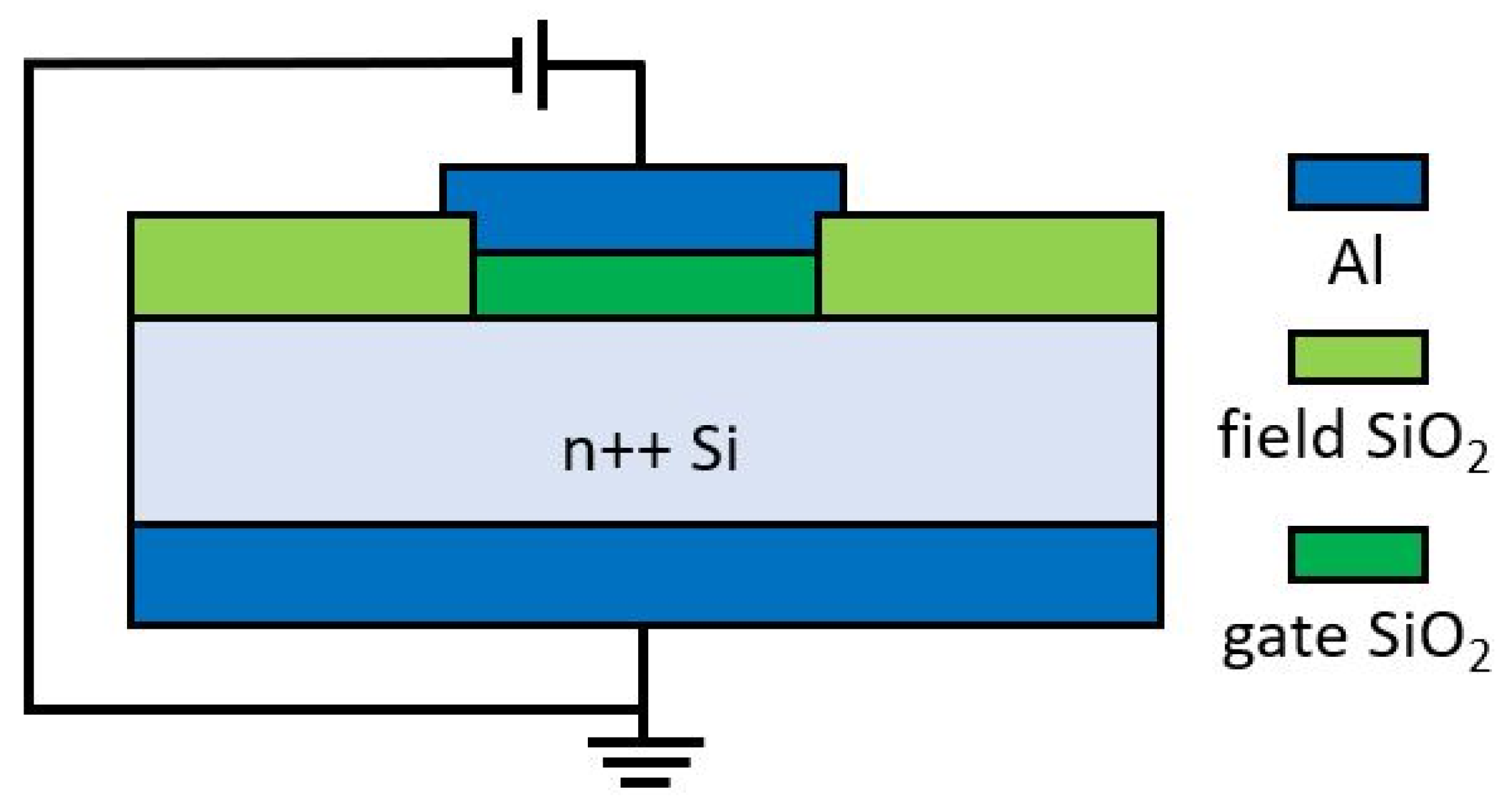
The MIS structures were fabricated using the standard CMOS-compatible processes. 2″ n-type highly doped (arsenic, resistivity less than 0.005 Ωcm) wafers were cleaned using the standard RCA method, and then, the wet oxidation process was carried out in a high-temperature furnace Thermco 2803 Furnace System. A photolithography process and wet etching were used to open windows in the field oxide. Wet etching was performed in a BHF solution. Then, 5–6 nm thin gate oxide was grown in a dry oxidation process (10 min at 820 °C). In the end, the Al top gate and bottom contact layers were deposited in magnetron sputtering processes and formed in the appropriate photolithography and etching processes. Structures were annealed in H2/Ar atmosphere at 400 °C for 30 min. A schematic picture of the fabricated structure is presented in Figure 1. Measurements were carried out using the Keithley 4200-SCS Semiconductor Characterization System (Keithley Instruments, LLC, Solon, OH, USA) with a Süss MicroTec PM8 low noise probe shield. DC measurements were performed with the static source-measure unit (SMU) connected to the device under test at room temperature. All studied devices were fabricated on the same wafer.
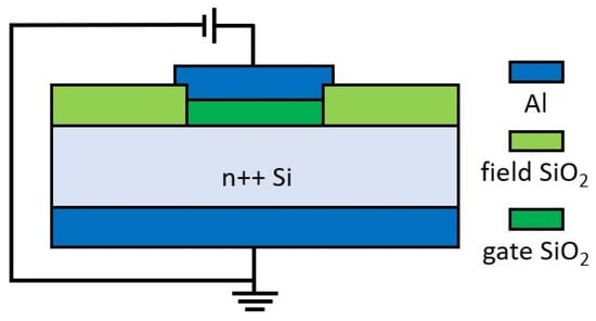
Figure 1.
Schematic picture of the measured structure (not to scale).
3. Results and Discussion
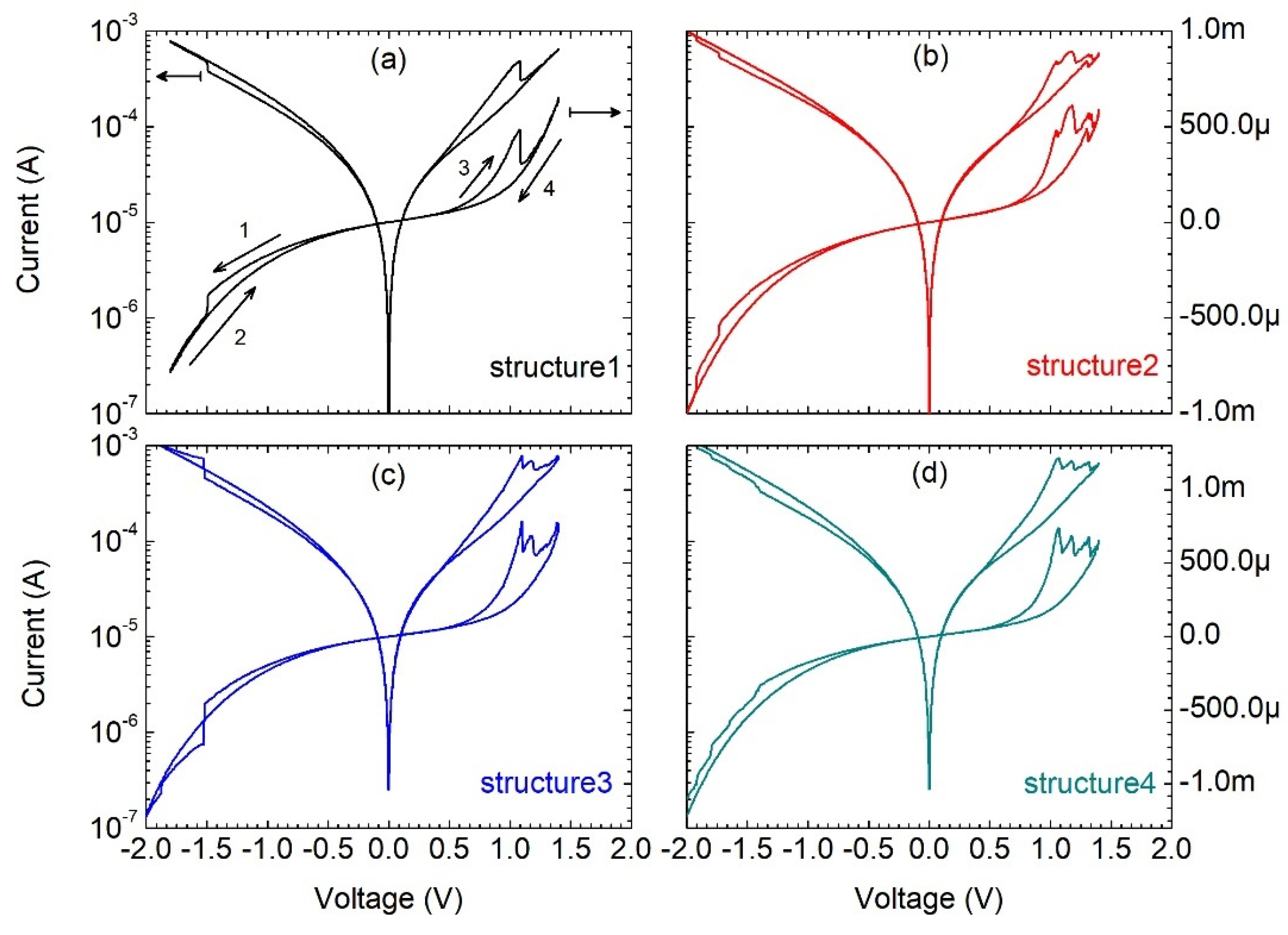
As discussed in the literature, transport through a dielectric can be controlled by various mechanisms [13,14,15], e.g., Poole–Frenkel, TAT, direct tunneling, Fowler–Nordheim tunneling, etc. Figure 2 shows the measured current–voltage characteristics in the logarithmic and linear scales for four different structures of the 156 μm gate diameter. The numbered arrows in Figure 2a indicate the measurement sequence.
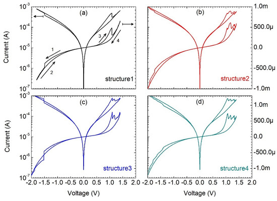
Figure 2.
Current–voltage characteristics of Al/SiO2/n++ Si structures (a–d) with a gate diameter of 156 um.
The devices present similar electrical characteristics exhibiting current–voltage hysteresis with a different number of features—sudden current rises at the negative gate voltages and current drops at the positive gate voltages. When the gate voltage increases, the current jumps to a new current–voltage dependence. The number of observed current rises at the negative gate bias coincides with the number of current drops at the positive gate bias.
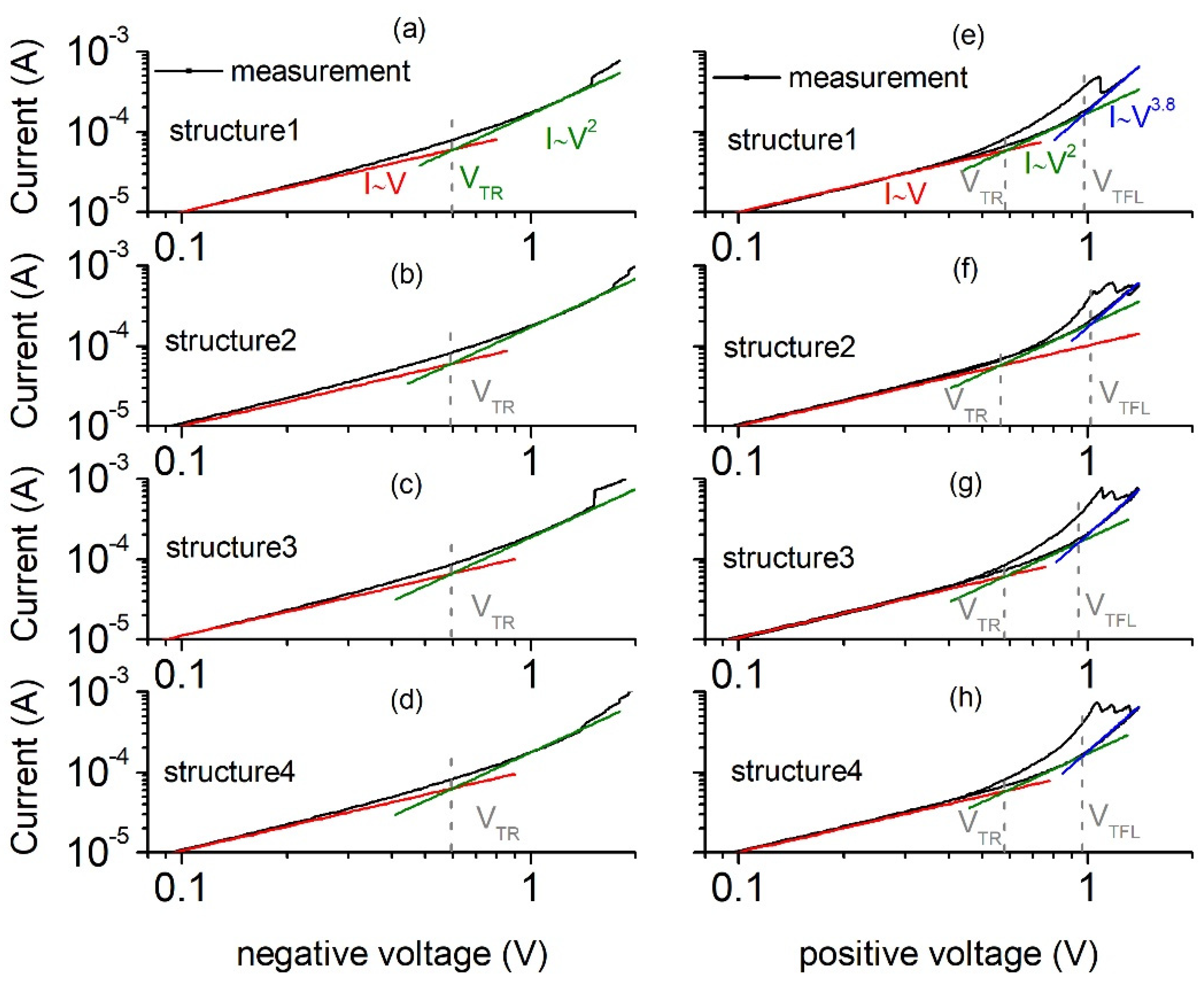
In order to examine the transport mechanism in the studied structures, the I-V characteristics of the same structures are plotted in Figure 3 in the log-log scale, together with fits of the slope in different voltage ranges. At the low voltage range, the current is proportional to the voltage, identifying the ohmic transport mechanism, whereas it changes to quadratic dependence at a given transition voltage VTR for both the positive and negative gate voltage polarizations. The parabolic dependence is related to the space-charge limited conduction through a region containing partially filled shallow traps [16]. Traps are being filled up, and only a fraction of the injected carriers enter the conduction band and contribute to the current. When increasing the positive voltage above VTFL, one can observe a higher-order current–voltage dependence (I~V3.8) for all measured structures. Fermi level moves upwards to near the conduction band of the dielectric, which results in an increase in the slope of the I-V dependence [15,17]. According to the SCLC theory with single-level shallow-trap centers, one can express the ohmic conduction current (JOhmic) at low voltages and the trap-filling component (JTFL) by the following formulas
where q is the electron charge constant, n0 is the free charge carrier concentration at thermal equilibrium, μ is the electron mobility in the dielectric, V is the applied voltage, d is the dielectric thickness, ε is the electric permittivity, and θ is the ratio of the free carrier density to the total carrier density (free and trapped). The VTR and VTFL voltages, which are marked in Figure 3, are given by
where Nt is the trap concentration in the dielectric. Values of VTR and VTFL for the considered structures and the concentration of traps in the oxide, extracted from Equation (4), are presented in Table 1.
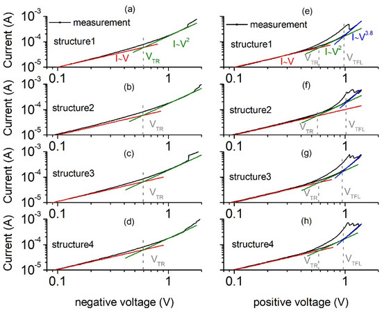
Figure 3.
Slope of the current–voltage characteristics in the log-log scale for different Al/SiO2/n++ Si structures for the negative (a–d) and positive (e–h) voltages.

Table 1.
Parameters obtained from I-V measurements, based on SCLC theory for different structures.
It is worth noticing that values of the trap concentration which were obtained for the positive voltages for different structures are similar. We do not observe VTFL transition points at negative voltages. Instead, sudden single or multiple current rises are observed, which cannot be explained using SCLC theory. We also observe current drops at the positive voltages. We suspect that such behavior might be related to the transport through deep trap levels instead of shallow traps.
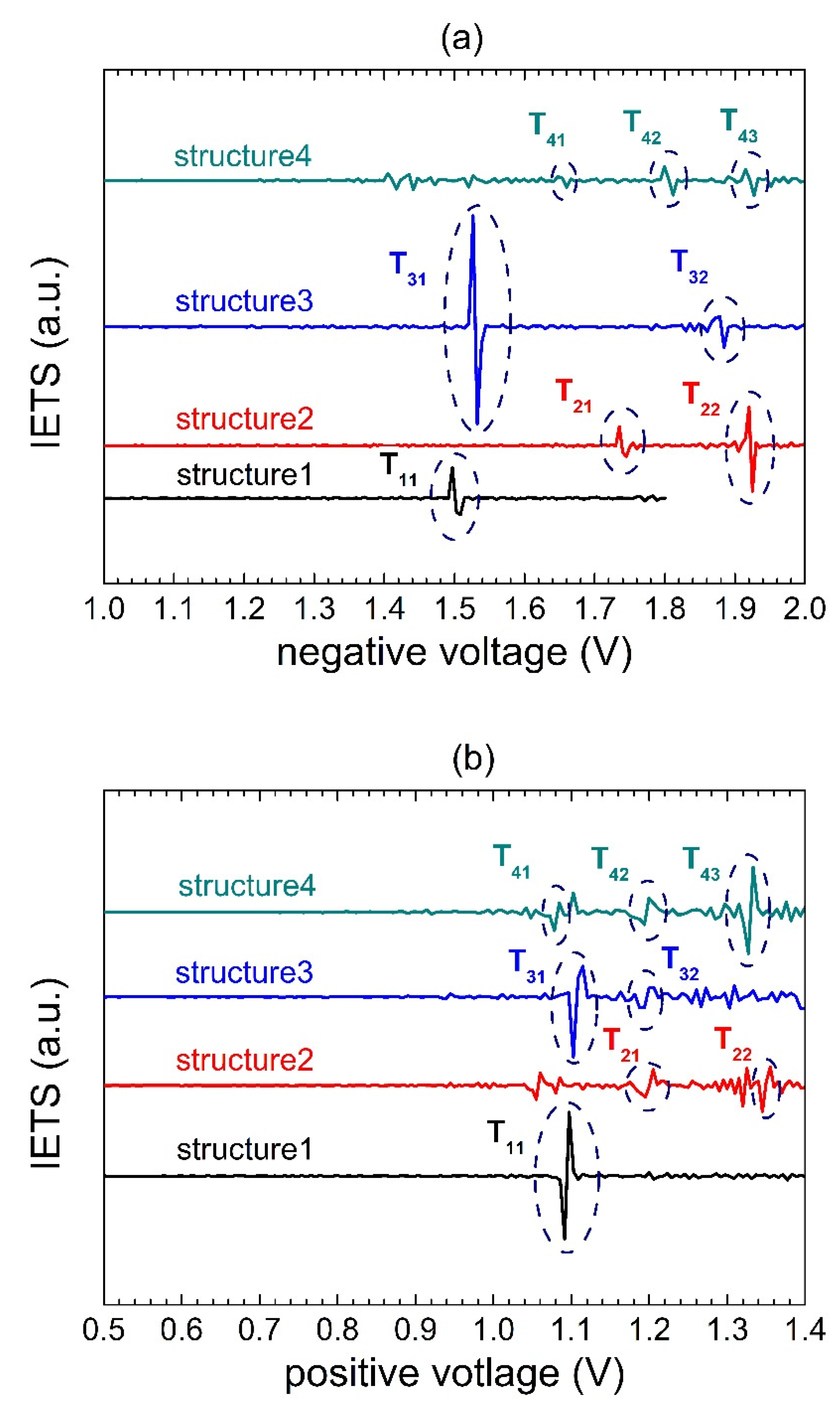
In order to understand these features, we analyzed the transport through the traps using inelastic electron tunneling spectroscopy (IETS). It is a technique that can be used to study phonons, bonding vibrations, and impurities [12,18] in MIM/MIS structures. It can also be helpful to analyze tunneling through traps in dielectrics [19,20], giving information about their geometrical position and energy. The IETS signal is proportional to the current’s second derivative, and it is usually measured using the lock-in amplifier to reduce the signal-to-noise ratio. However, the observed features are clearly strong in our case, and we calculated the IETS signal straightforwardly from the I-V curves. The results are presented in Figure 4.
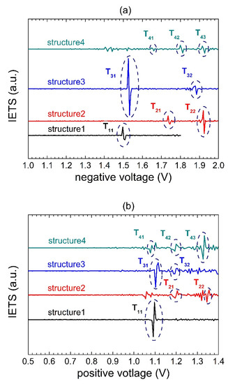
Figure 4.
IETS signal of Al/SiO2/n++ Si structures for the negative (a) and positive (b) voltages.
According to IETS theory [21], the shape of the signal can be related to the trap-assisted tunneling process or to the charge-trapping process. The relevant features are marked in Figure 4. We observe peak-to-valley shape signals associated with trap-assisted tunneling at the negative voltage values. Their occurrence corresponds to the voltages at which sudden current bumps appear in Figure 3a–d. For the positive voltages, we observe the valley-to-peak shape signals, which are usually attributed to the charge-trapping process [12]. We attribute these features rather to the blockage of the trap-assisted tunneling path, as will be shown later. Other less distinct features are visible in Figure 4 at lower voltages, which we ascribe to the shallow traps related to SCLC transport.
It has been shown [22] that positions of the peak-to-valley and valley-to-peak signals are related to the position xt of traps within the dielectric (the effective electrical distance from the oxide/metal gate interface) and the relative energy of the deep trap level Et = qVt above the Fermi level at the zero bias
where Vp and Vn are the absolute values of the voltages for the positive and negative gate bias, respectively, at which the corresponding trap features are observed, and tox is the oxide thickness. Table 2 shows the values of xt and Et, obtained for the investigated structures using Equations (5) and (6).
Table 2.
Relative position and energy of deep trap levels for different structures.
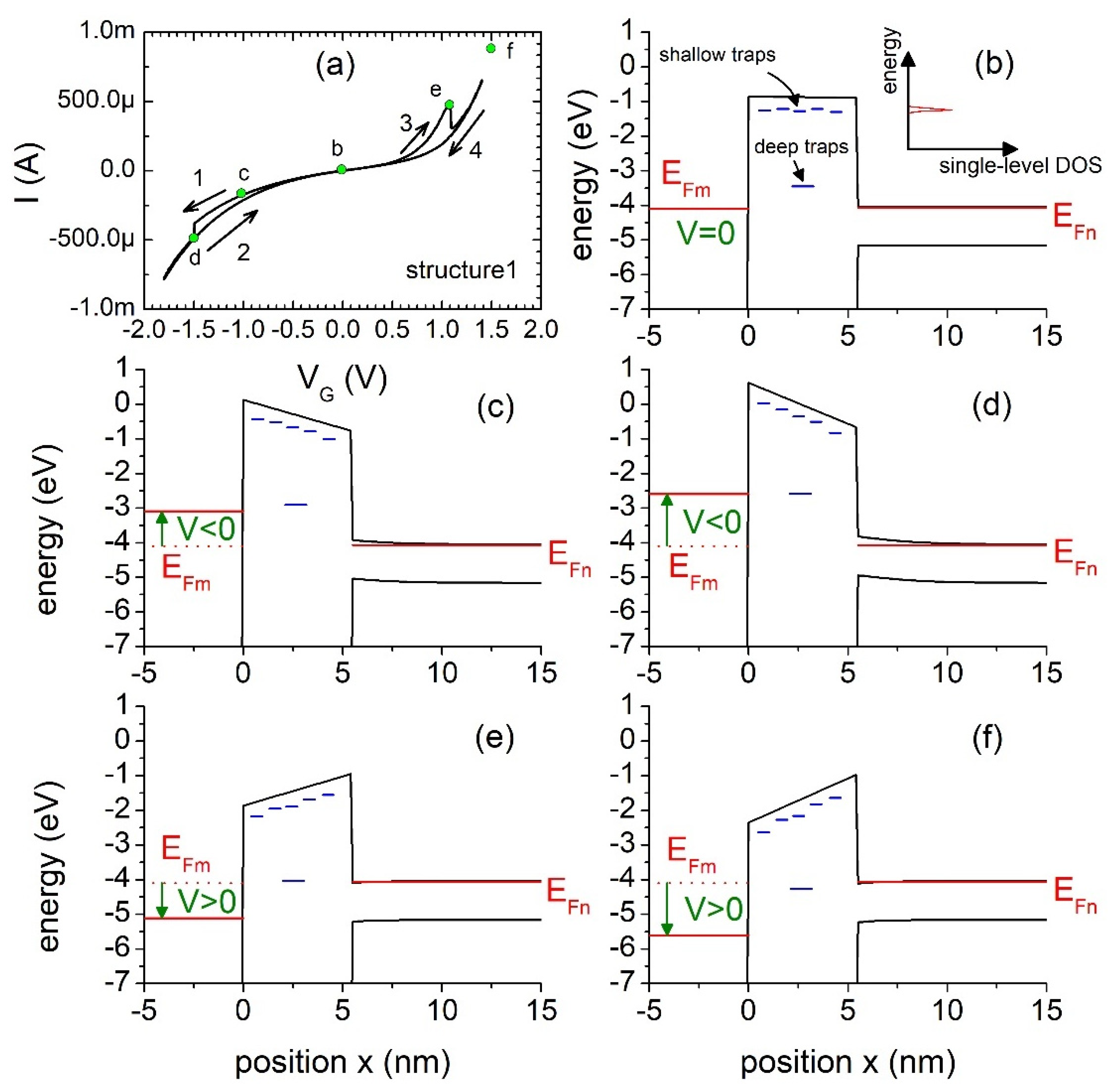
A number of trap levels can differ for different structures. Irrespective of this, the relative trap position does not change significantly, regardless of the trap energy, as well as the energy levels of the deep traps being similar for different structures. In order to analyze the I-V hysteresis and explain sudden current changes at the Vp and Vn points, the energy band diagrams of the investigated structure were calculated by using a 1D Poisson–Schrödinger solver. We assumed tox = 5.5 nm, whereas other parameters used in electrostatics simulations were typical for the Al/SiO2/Si system.
Figure 5 shows the energy band diagrams calculated for different bias conditions. Shallow trap levels participating in the SCLC transport are schematically added. We also added a deep trap energy level T11 calculated for structure no. 1. At sufficiently high negative voltage bias, one can observe that the position of the metal Fermi level EFm coincides with the position of the energy trap level. As a result, a sudden increase in the current is observed due to the possibility of the trap-assisted tunneling of electrons from the metal gate to the semiconductor conduction band. The electron charge is accumulated in the deep traps, and the charge de-trapping process is long enough to sustain the electrostatic effect during measurements. Thus, a different current–voltage dependence is observed when going back from the negative bias range to the positive bias range. The charge stored in the traps can contribute to the total current via tunneling to the metal or the semiconductor regions, provided that free states are available. Moreover, trap-assisted tunneling can also occur at a positive bias. At a given voltage Vp, a sudden current drop related to the blockage of the trap-assisted tunneling path can be observed. Such a situation is depicted in Figure 5e. The deep trap energy level position aligns with the bottom of the conduction band. At a slightly higher gate voltage, the energy level Et lies in the range of the semiconductor bandgap, and trap-assisted tunneling is forbidden. The SCLC current dominates the deep trap-assisted tunneling current at small bias voltages (|V| < 0.7 V), regardless of the bias direction. The trapped charges modify the potential barrier electrostatically and affect the resultant transport process.
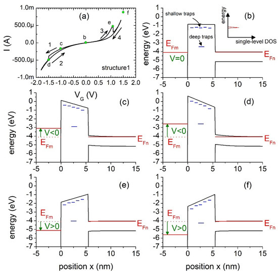
Figure 5.
Energy band diagrams of the MIS structure no. 1 with marked trap energy levels in the dielectric for V = 0 (b), V < 0 (c,d) and V > 0 (e,f). Shallow trap levels are shown schematically, whereas the deep trap energy level position is calculated. Points corresponding to the band diagrams were marked in (a).
In our opinion, the proposed mechanisms can explain the hysteresis effects observed on the current–voltage characteristics of the investigated devices very well. The traps in the SiO2 layer might come from the silicon oxidation process of a highly doped silicon substrate. We have not observed the hysteresis effect in structures fabricated with the same process flow on wafers with low doping levels (ρ = 1–10 Ωcm). A very high doping level has a pronounced effect on the oxidation rate and the resultant material stress during the process. Moreover, due to the redistribution of dopants during the oxidation process, the formed oxide can absorb the dopants from silicon, causing material defects. All these factors can affect the material quality and be the origin of traps.
4. Conclusions
This work shows that SiO2-based metal–insulator–semiconductor devices with highly doped silicon substrates can exhibit hysteresis effects. We analyzed the current–voltage characteristics of the fabricated devices and identified the transport mechanisms. We evaluated the trap concentration and identified deep trap energy levels and their position within the dielectric layer. We showed that I-V hysteresis could be related to the trap-assisted tunneling through these defects and the charge trapping effect.
Author Contributions
Conceptualization, P.W.; methodology, P.W.; validation, P.W. and B.M.; formal analysis, P.W.; investigation, P.W. and B.M.; resources, P.W.; data curation, P.W.; writing—original draft preparation, P.W.; writing—review and editing, P.W. and B.M.; visualization, P.W.; supervision, P.W. and B.M.; project administration, P.W. All authors have read and agreed to the published version of the manuscript.
Funding
This research was funded by the National Science Centre, Poland, grant number 2018/31/N/ST7/01147.
Institutional Review Board Statement
Not applicable.
Informed Consent Statement
Not applicable.
Data Availability Statement
The data presented in this study are available on request from the corresponding author.
Conflicts of Interest
The authors declare no conflict of interest.
References
- Molas, G.; Nowak, E. Advances in Emerging Memory Technologies: From Data Storage to Artificial Intelligence. Appl. Sci. 2021, 11, 11254. [Google Scholar] [CrossRef]
- Chang, T.C.; Chang, K.C.; Tsai, T.M.; Chu, T.J.; Sze, S.M. Resistance random access memory. Mater. Today 2016, 19, 254–264. [Google Scholar] [CrossRef]
- Grenouillet, L.; Francois, T.; Coignus, J.; Kerdiles, S.; Vaxelaire, N.; Carabasse, C.; Mehmood, F.; Chevalliez, S.; Pellissier, C.; Triozon, F.; et al. Nanosecond Laser Anneal (NLA) for Si-implanted HfO2 Ferroelectric Memories Integrated in Back-End of Line (BEOL). In Proceedings of the 2020 IEEE Symposium on VLSI Technology, Honolulu, HI, USA, 16–19 June 2020. [Google Scholar] [CrossRef]
- Wang, Z.; Hao, X.; Xu, P.; Hu, L.; Jung, D.; Kim, W.; Satoh, K.; Yen, B.; Wei, Z.; Wang, L.; et al. STT-MRAM for Embedded Memory Applications. In Proceedings of the 2020 IEEE International Memory Workshop (IMW), Dresden, Germany, 17–20 May 2020. [Google Scholar] [CrossRef]
- Vexler, M.; Shulekin, A.; Grgec, D.; Grekhov, I.; Meinerzhagen, B. Band-to-band tunneling related effects in a thin MOS structure. Microelectron. Eng. 2004, 72, 180–184. [Google Scholar] [CrossRef]
- Kareva, G.G.; Vexler, M.I. Simulation of electron transport in metal/high-k-oxide/SiO2/p+Si resonant-tunneling diodes. Microelectron. Eng. 2015, 147, 223–226. [Google Scholar] [CrossRef]
- Vexler, M.I. Enhancement of minority carrier supply in a resonant-tunneling metal-insulator-silicon capacitor. J. Appl. Phys 2017, 121, 155702. [Google Scholar] [CrossRef]
- Sun, J.P.; Haddad, G.I.; Mazumder, P.; Schulman, J.N. Resonant tunneling diodes: Models and properties. Proc. IEEE 1998, 86, 641–660. [Google Scholar] [CrossRef] [Green Version]
- Wisniewski, P.; Majkusiak, B.; Stonio, B. Tunneling and Resonant Tunneling Effects in the Metal-Ultrathin Oxide-(n+)Silicon Structures. In Proceedings of the 2020 Joint International EUROSOI Workshop and International Conference on Ultimate Integration on Silicon (EUROSOI-ULIS), Caen, France, 1–30 September 2020. [Google Scholar] [CrossRef]
- Wiśniewski, P.; Jasiński, J.; Mazurak, A.; Stonio, B.; Majkusiak, B. Investigation of Electrical Properties of the Al/SiO2/n++-Si Resistive Switching Structures by Means of Static, Admittance, and Impedance Spectroscopy Measurements. Materials 2021, 14, 6042. [Google Scholar] [CrossRef] [PubMed]
- Reed, M.A. Inelastic electron tunneling spectroscopy. Mater. Today 2008, 11, 46–50. [Google Scholar] [CrossRef]
- Kim, Y.; Chang, S.W. Inelastic Electron Tunneling Spectroscopy: Investigation of Bulk Dielectrics and Molecules. IEEE Trans. Electron Devices 2021, 68, 1411–1419. [Google Scholar] [CrossRef]
- Chiang, T.H.; Wager, J.F. Electronic conduction mechanisms in insulators. IEEE Trans. Electron Devices 2018, 65, 223–230. [Google Scholar] [CrossRef]
- Lim, E.W.; Ismail, R. Conduction Mechanism of Valence Change Resistive Switching Memory: A Survey. Electronics 2015, 4, 586–613. [Google Scholar] [CrossRef]
- Chiu, F.C. A review on conduction mechanisms in dielectric films. Adv. Mater. Sci. Eng. 2014, 578168. [Google Scholar] [CrossRef] [Green Version]
- Zhang, P.; Ang, Y.S.; Garner, A.L.; Valfells, Á.; Luginsland, J.W.; Ang, L.K. Space-charge limited current in nanodiodes: Ballistic, collisional, and dynamical effects. J. Appl. Phys 2021, 129, 100902. [Google Scholar] [CrossRef]
- Vasileiadis, N.; Karakolis, P.; Mandylas, P.; Ioannou-Sougleridis, V.; Normand, P.; Perego, M.; Komninou, P.; Ntinas, V.; Fyrigos, I.A.; Karafyllidis, I.; et al. Understanding the Role of Defects in Silicon Nitride-Based Resistive Switching Memories through Oxygen Doping. IEEE Trans. Nanotechnol. 2021, 20, 356–364. [Google Scholar] [CrossRef]
- Ma, T.P.; He, W.; Wang, M. Inelastic Electron Tunnelling Spectroscopy (IETS) of High-k Dielectrics. AIP Conf. Proc. 2005, 788, 73. [Google Scholar] [CrossRef] [Green Version]
- Reiner, J.W.; Cui, S.; Liu, Z.; Wang, M.; Ahn, C.H.; Ma, T.P. Inelastic Electron Tunneling Spectroscopy Study of Thin Gate Dielectrics. Adv. Mater. 2010, 22, 2962–2968. [Google Scholar] [CrossRef] [PubMed]
- Lee, D.; Park, J.W.; Cho, N.K.; Lee, J.; Kim, Y.S. Verification of Charge Transfer in Metal-Insulator-Oxide Semiconductor Diodes via Defect Engineering of Insulator. Sci. Rep. 2019, 9, 1–9. [Google Scholar] [CrossRef] [PubMed] [Green Version]
- He, W.; Ma, T.P. Inelastic electron tunneling spectroscopy study of traps in ultrathin high-k gate dielectrics. Appl. Phys. Lett. 2003, 83, 5461. [Google Scholar] [CrossRef]
- Liu, Z.; Ma, T.P. Determination of energy and spatial distributions of traps in ultrathin dielectrics by use of inelastic electron tunneling spectroscopy. Appl. Phys. Lett. 2010, 97, 172102. [Google Scholar] [CrossRef]
Publisher’s Note: MDPI stays neutral with regard to jurisdictional claims in published maps and institutional affiliations. |
© 2022 by the authors. Licensee MDPI, Basel, Switzerland. This article is an open access article distributed under the terms and conditions of the Creative Commons Attribution (CC BY) license (https://creativecommons.org/licenses/by/4.0/).