Article

Fluorine-Terminated Polycrystalline Diamond Solution-Gate Field-Effect Transistor Sensor with Smaller Amount of Unexpectedly Generated Fluorocarbon Film Fabricated by Fluorine Gas Treatment

by
Yukihiro Shintani
1,2,* and
Hiroshi Kawarada
1,3
1
Graduate School of Science and Engineering, Waseda University, 3-4-1 Okubo, Shinjuku, Tokyo 169-8555, Japan
2
Department of Management Information Sciences, Faculty of Social Systems Science, Chiba Institute of Technology, 2-17-1 Tsudanuma, Narashino, Chiba 275-0016, Japan
3
The Kagami Memorial Laboratory for Materials Science and Technology, Waseda University, 2-8-26 Nishiwaseda, Shinjuku, Tokyo 169-0051, Japan
*
Author to whom correspondence should be addressed.
Materials 2022, 15(9), 2966; https://doi.org/10.3390/ma15092966
Submission received: 6 March 2022 / Revised: 15 April 2022 / Accepted: 17 April 2022 / Published: 19 April 2022

Abstract

:
In this study, a partially fluorine-terminated solution-gate field-effect transistor sensor with a smaller amount of unexpectedly generated fluorohydrocarbon film on a polycrystalline diamond channel is described. A conventional method utilizing inductively coupled plasma with fluorocarbon gas leads the hydrogen-terminated diamond to transfer to a partially fluorine-terminated diamond (C–F diamond); an unexpected fluorohydrocarbon film is formed on the surface of the diamond. To overcome this issue, we newly applied fluorine gas for the fluoridation of the diamond. Analytical results of X-ray photoelectron spectroscopy and time-of-flight secondary ion mass spectrometry suggest that the fluorocarbon film does not exist or only a smaller amount of fluorocarbon film exists on the diamond surface. Conversely, the C–F diamond fabricated by the conventional method of inductively coupled plasma with a perfluoropropane gas (C3F8 gas) source possesses a certain amount of fluorocarbon film on its surface. The C–F diamond with a smaller amount of unexpectedly generated fluorohydrocarbon film possesses nearly ideal drain–source–voltage vs. gate–source–current characteristics, corresponding to metal–oxide–silicon semiconductor field-effect transistor theory. The results indicate that the fluorine gas (F2 gas) treatment proposed in this study effectively fabricates a C–F diamond sensor without unexpected semiconductor damage.

1. Introduction

The surface modification of diamond is an effective means of controlling its physical/chemical properties, i.e., biological affinity, friction, electrical/electrochemical properties, wettability [1]. Plasma treatment is one of the most efficient methods for the introduction of a heteroatom onto the surface of a diamond within a shorter time, including a chlorine termination (C–Cl termination) using chloride gas (Cl2 gas) [2], an oxygen termination (C–O termination) using oxygen gas (O2 gas) [3,4], and a hydrogen termination (C–H termination) using hydrogen gas (H2 gas) [5,6,7], respectively. The surface of a fluorine-terminated diamond (C–F diamond) is attractive because of its unique properties, i.e., low coefficient of friction, hydrophobicity, and chemical/biochemical inertness [8,9,10,11,12,13,14]. In addition, the diamond fluorination increases the overpotential of hydrogen evolution reactions in electrolyte aqueous solutions, where it could be an advantage for sensor use [14,15].
Authors and our group successfully induced diamond semiconductors for a no-gate-insulator SGFET (electrolyte-solution-gate field-effect transistor) utilizing a single-crystal diamond [16,17,18,19], a polycrystalline diamond [12,20,21], and a boron-doped diamond [12,20,22]. An electric double layer on the diamond surface leads to its operation as a gate insulator in these devices [16]. A partially oxygen-terminated diamond (C–O diamond) and partially nitrogen-terminated diamond (C–N diamond) have also been successfully induced to control ion sensitivity for sensors [22]. Since its specific properties, such as hydrophobicity, the C–F diamond surface has also become a focus of attention for the use of diamond SGFET sensors. The C–F surface decreases its pH sensitivity compared with C–H, C–O, and C–N diamond surfaces [12]. Various types of C–F diamond fabrication methods have been presented, i.e., exposure to dissociated xenon difluoride (XeF2) [23,24] or inductively coupled plasma (ICP) treatment with a fluorocarbon gas (CxFy gas) source [12]. However, in addition to the well-known issue in which ICP with CxFy gas could cause damage to the quality of the crystal structure and surface smoothness [7], the fluorination process of ICP–CxFy can form an unexpected fluorohydrocarbon film (CxFy film) on the diamond surface, where it could influence its field-effect transistor current–voltage (FET-IV) characteristics if used as a semiconductor chemical sensor.
Here, to overcome the above-mentioned issues, we propose a “fluorine gas direct treatment method” utilizing fluorine gas (F2 gas) for the fabrication of a no-gate-insulator diamond SGFET sensor with a smaller amount of unexpectedly generated fluorocarbon film. X-ray photoelectron spectroscopy (XPS) and time-of-flight secondary ion mass spectrometry (TOF-SIMS) were used to investigate the state of the fluorohydrocarbon film on the surface of the C–F diamond, and the current–voltage (IV) characteristics of the diamond FETs created by the fluorine gas direct treatment were also evaluated.

2. Materials and Methods

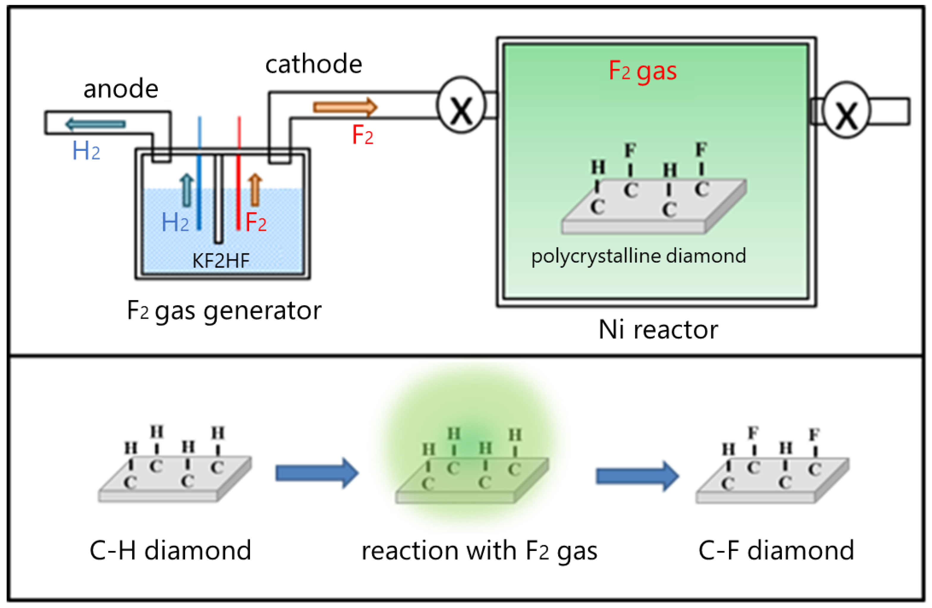
2.1. Fabrication of C–F Diamonds

Highly (110)-oriented polycrystalline diamonds that were synthesized by chemical vapor deposition (CVD) were used in this study. The typical specification of the (110) diamond is described in our previous study [25]. Before use, the (110) diamonds were cleaned with ultrapure water, ethanol, acetone, and isopropyl alcohol [25,26]. To obtain a nearly full C–H diamond surface that could be used for fluorination, a hydrogen termination was conducted with an “Applied Science and Technology (ASTeX)-type” microwave plasma chemical vapor deposition system (Brighton, MI, USA).
To obtain the C–F diamond surface with a smaller amount of unexpectedly generated CxFy film, a F2 gas treatment was introduced, where some of the experiments were conducted in collaboration with the F-Technical Assistance Center, TAKAMATSU TEISAN Corporation. Figure 1 shows a schematic diagram of the process of the F2 gas treatment method. The process was carried out by using a lab-made nickel (Ni) reactor or a F2 reactor. The nearly full C–H diamond substrates were set in the reactor and then the pressure in the reactor was reduced after a purge of argon gas. After decompression, F2 gas that was generated by electrolysis of potassium diacid fluoride (KF2HF) melted at ca. 100 degrees Celsius (degrees C) was introduced into the Ni reactor. After the F2 treatment, the reactor was cooled down to room temperature, and then F2 gas in the reactor was purged out with argon gas. The fluorine pressure for the reaction was ca. 101 kPa, and the reaction time was from 30 min to 24 h.
For comparison, conventional ICP treatment with perfluoropropane gas (C3F8 gas) was applied for the fabrication of C–F diamonds under pressure of 3 Pa and the gas flow of 20 standard cubic centimeters per minute (sccm) with 100–500 W for up to 30 s. To characterize the C–F diamond surface as an SGFET sensor, a boron-doped diamond (BDD) SGFET was fabricated in the same process described in our previous works [12,20].

2.2. Characterization of C–F Diamond Surface and Diamond SGFET

A Model 3300 X-ray photoemission spectroscopy (XPS; ULVAC-Phi) device was used for the identification of chemical bonds (C–F, C–O, C–N) on the diamond surface. The functional groups on the diamond were also analyzed by using a Model TRIFT III TOF–SIMS (ULVAC PHI) device. The typical conditions were as follows: the primary ion source was gallium ions; the ion irradiation time was 300 s; the impact energy was 15 kV; the measured mass range was 0.1–200; the mass resolution was 500 at m/z; and the lateral resolution was 22 μm. Curve fitting of XPS spectra was performed with the analysis software Origin.
The C–F BDD SGFETs were characterized using a measurement system comprising two sets of Model 2400 source-measure units (Keithley Instruments, Inc., Cleveland, OH, USA) and/or two sets of Model GS820 source-measure units (Yokogawa Electric Corp., Tokyo, Japan) for the gate-source voltage (Vgs) and the application of the drain-source voltage (Vds) with common-source mode. Labview 2010 (National Instruments Inc., Austin, TX, USA) was used to control the process and obtain the I–V data. The gate-source voltage was applied via a silver–silver chloride gate electrode (Ag/AgCl electrode). SGFET I–V profiles were obtained at room temperature (approximately 20 degrees C). All chemicals used in this study were of reagent grade and were obtained from Wako, Kanto Kagaku, Tokyo Kasei, and Horiba. Additionally, 1 mM phosphate-buffered saline buffer solution (PBS; pH 7.4) was used for the evaluation.

3. Results

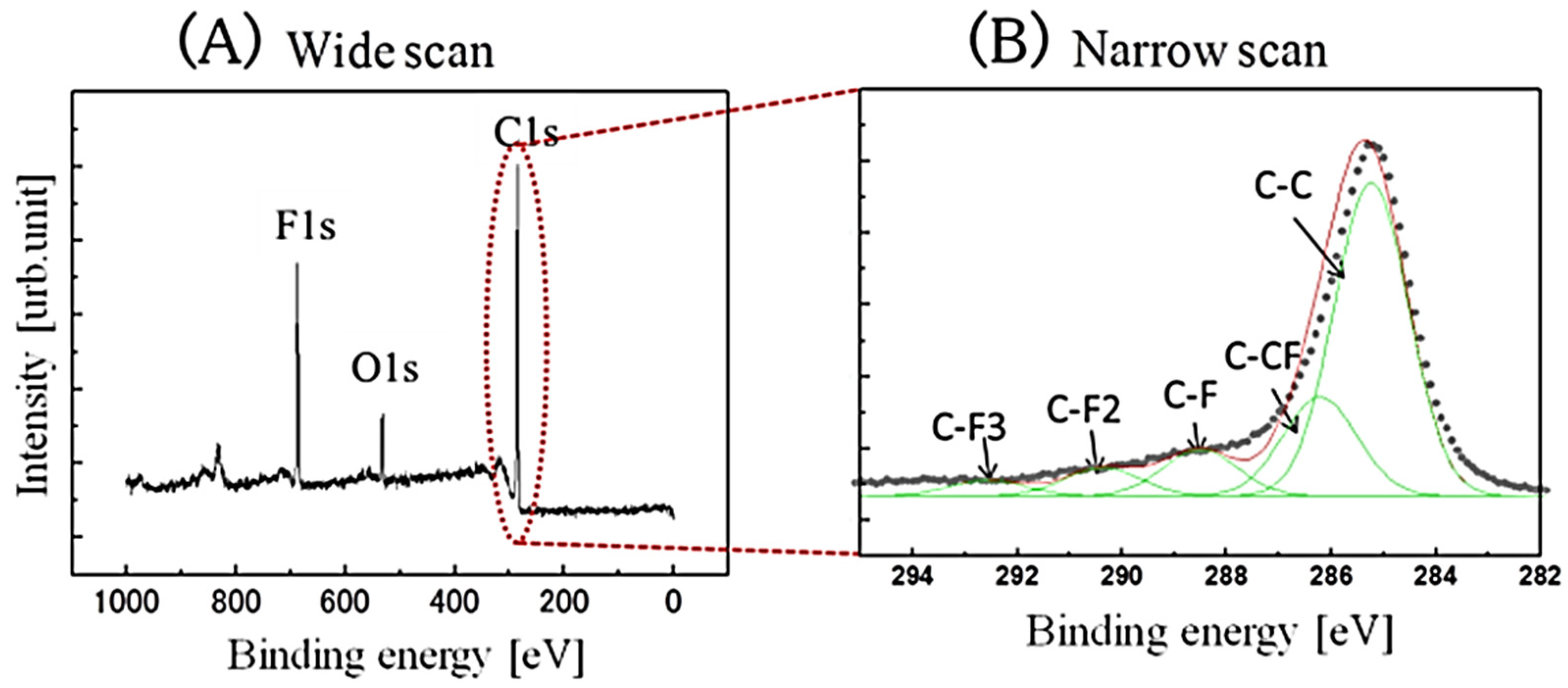
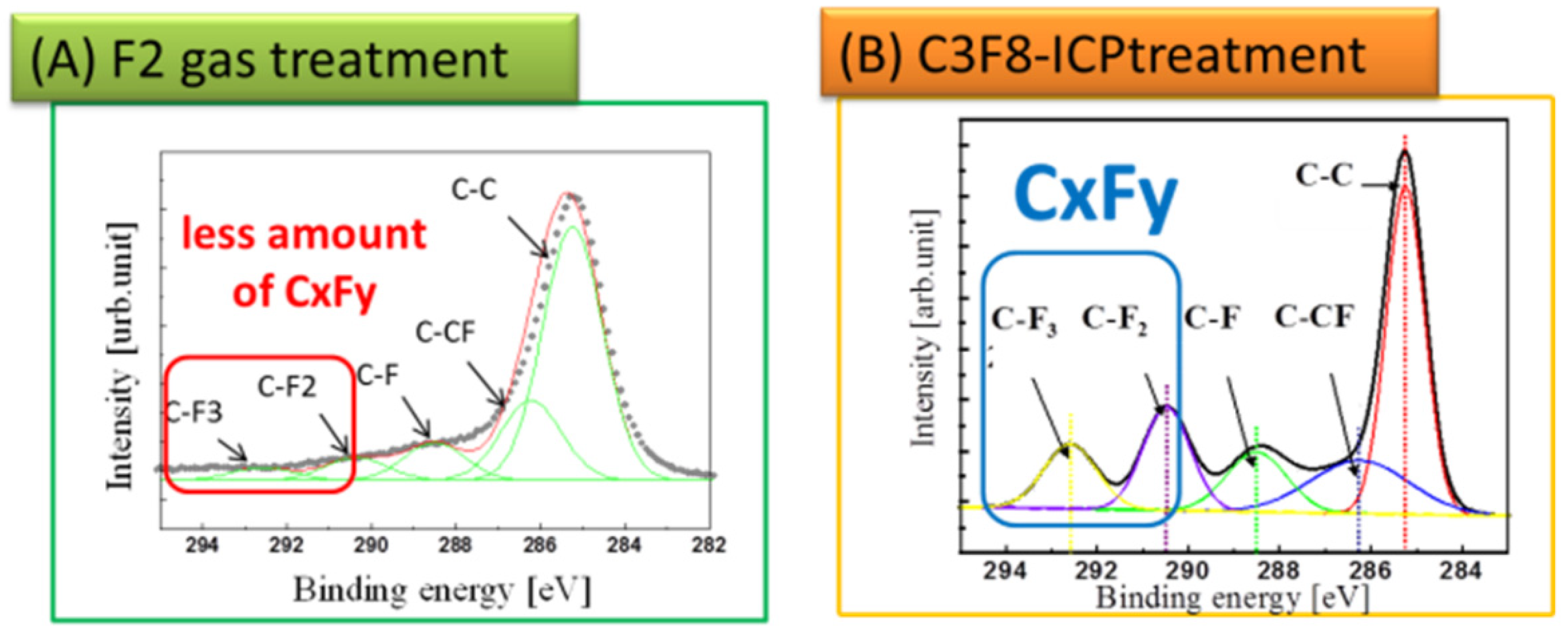
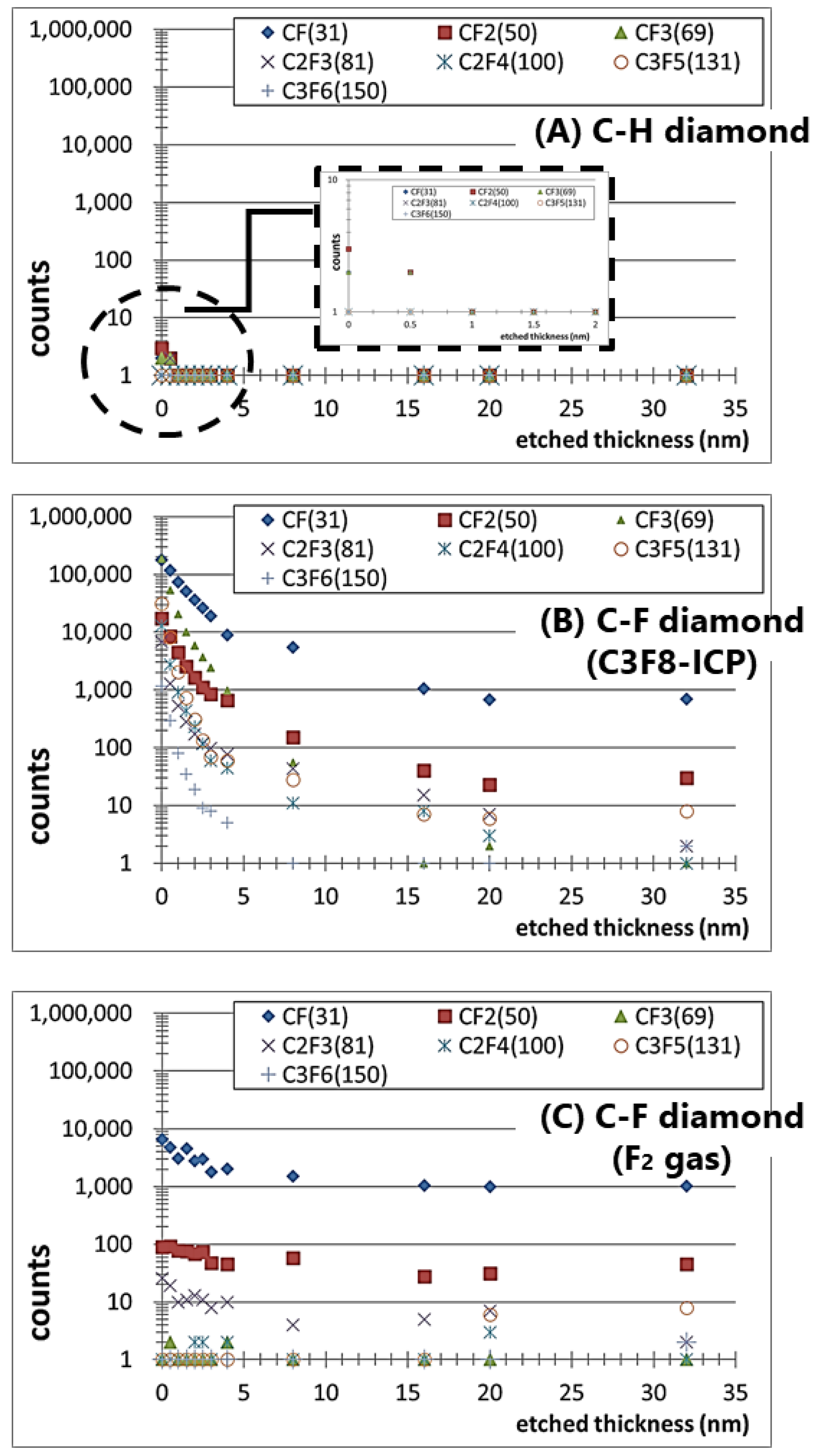
3.1. Characterization of the C–F Diamond

To evaluate the diamond surfaces after the F2 reaction, the fluorine functional groups on the C–F diamond surfaces were analyzed using XPS with a monochromated Al K X-ray source. The coverage of fluorine (F1s; 688 eV) was estimated from the deconvolution of the C 1s peak intensity. The wide spectra in Figure 2A reveal the elemental composition on the C–F diamond films after the direct F2 gas functionalization of the surface. The oxygen species existing on the C–F diamond surface may be attributed to physio-adsorbed oxygen after several days of exposure to the air following the C–F treatment. No additional treatment was performed to remove the physio-adsorbed oxygen effect prior to the XPS analysis. The main peak near 284.5 eV is the C 1s peak. The F 1s peak at 688 eV in the spectrum of the F2 direct fluorination confirms the surface fluorination of the diamond films. The deconvolutions of the C 1s spectra on the F2 direct fluorination are shown in Figure 2B. The deconvolutions can be separated into sp3C (285 eV), C–CF (286.6 eV), C–F (288.8 eV), C–F2 (290.9 eV), and C–F3 (292.8 eV). The amount of fluorocarbon layers can then be evaluated, in particular, using the amounts of C–F2 and C–F3 bonds on the diamond surfaces. Figure 3 shows the deconvoluted C 1s of the XPS narrow analysis on the C–F diamonds. Figure 3 shows the C–F diamonds treated by F2 gas and C3F8-ICP. The respective percentages (%) of various types of chemical functionalization derived from the fluorine functional groups on the C–F diamonds were calculated from Figure 3A,B, as summarized in Table 1. In addition, Figure 4 shows a schematic diagram of the proposed surface state of the C–F diamonds, reflecting the XPS analysis results (Figure 3 and Table 1). Because a smaller amount of C–F3 was estimated in comparison to C–CF2 and C–F on the F2-treated C–F diamonds, a fluorocarbon film did not exist or only small amounts existed on the surfaces. However, because the amount of C–F3 was nearly the same as that of C–CF2 and C–F, a certain amount of fluorocarbon film was present on the surfaces of the C–F diamonds treated by C3F8-ICP.
To verify the model in Figure 4, fluorine-related fragments delivered from the fluorine-terminated group and the fluorocarbon films of the C–F diamonds fabricated using F2 gas and C3F8-ICP were analyzed via TOF-SIMS to confirm the presence of fluorohydrocarbons on the C–F diamonds. A C–H diamond was used as a reference sample. Figure 5 shows the detected amount of various fluorocarbon secondary ions in the range of 0–200 amu, where each count was collected under the same conditions (i.e., primary ion dose density, same sample area size, and same beam condition). The fluorocarbon-related fragment peaks are CF + (m/z 31), CF2 + (m/z 50), CF3 + (m/z 69), C2F3 + (m/z 81), C2F4 + (m/z 100), C3F5 + (m/z 131), and C3F6 + (m/z 150). Even though the fluorocarbon-related fragments are nearly undetectable in the case of the C–H diamond (Figure 5A), the C–F diamonds have fluorocarbon-related fragments on the surface and at depth (Figure 5B,C). The detection of CF3+ fragments suggests the presence of fluorohydrocarbons on the surfaces of the ICP-treated C–F diamonds. In Figure 6B, the amount of CF3+ fragment decreases at greater depths from the substrate surface, and the ratio of fluorine-related fragments becomes essentially constant at the depth where the amount of CF3+ fragment is sufficiently reduced. This indicates that fragments derived from the fluorocarbon film are detected on the surface of the substrate but, as the depth increases, fragments derived from the fluorine termination of the diamond substrate are detected. Conversely, Figure 5C shows that the CF3+ fragment is not detected on the surface and that the ratio of fluorine-related fragments becomes essentially constant away from the surface. This indicates that a fluorocarbon film does not exist or only small amounts exist on the surfaces of C–F diamonds treated via F2 gas reaction.

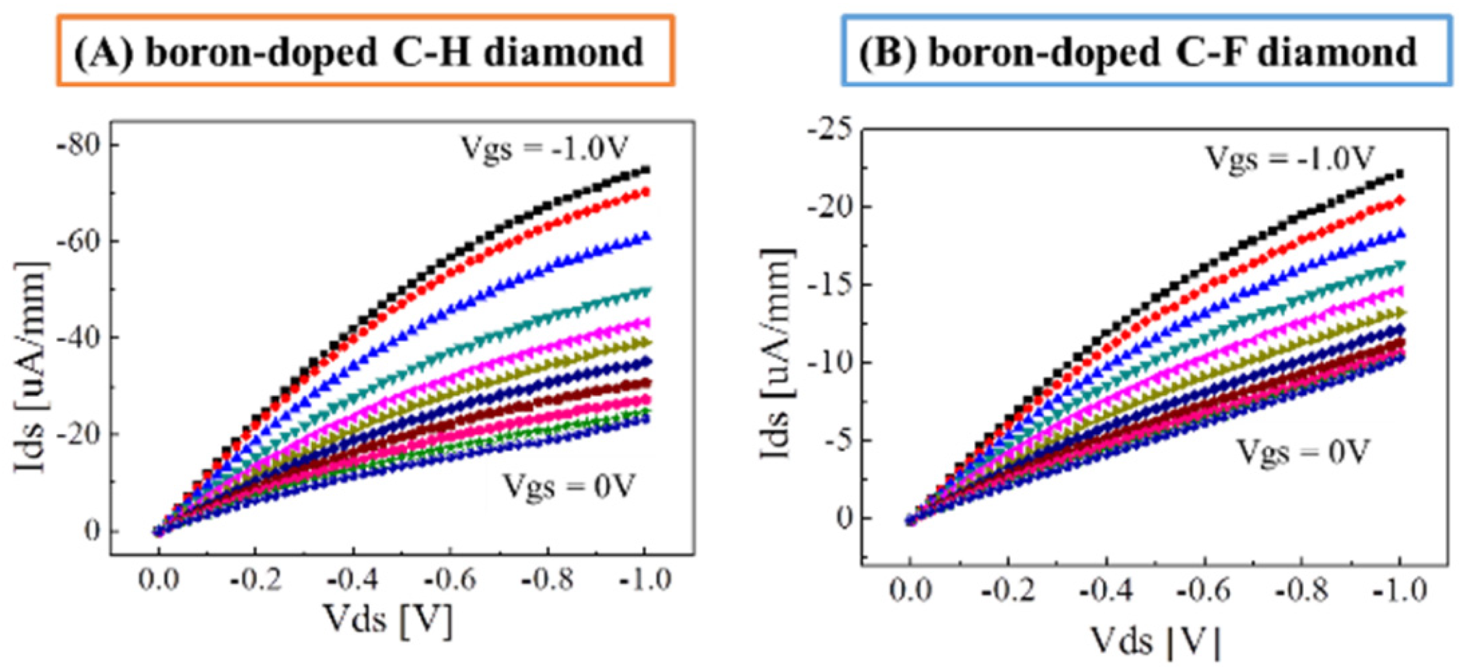
3.2. Characterization of C–F BDD SGFET

For a feasibility study of C–F BDD SGFET as a chemical sensor, the FET current–voltage (FET I–V) characterization of the C–F BDD SGFET was examined with respect to the C–H BDD SGFET. Initially, the SGFETs and an Ag–AgCl gate electrode (the reference electrode) were washed with ultrapure water and then immersed in a 1 M PBS buffer solution (pH 7.4) for 30 min before their FET I–V characteristics were evaluated using a common-source method via drain-source current (Ids)–gate-source (Vgs) characteristics (the so-called static characteristics). Figure 6 shows typical characteristics of the drain-source voltage (Vds) and drain-source current (Ids) of the developed SGFETs. Figure 6A,B show the static characteristics of the C–H BDD SGFET and the C–F BDD SFGET fabricated via F2 gas direct fluorination, respectively. The Vgs applied through the Ag–AgCl gate electrode was varied stepwise from −1.0 V to 0 V in steps of 100 mV. For each value of Vgs, the Ids was obtained as a function of the Vds from 0 V to −1.0 V. The drain-source current was pinched off, and the saturation regions and the distinct linear pattern were obtained. Under the condition of Vds of −1.0 V, the Ids of the C–H diamond is −22 μA/mm, whereas the Ids of the fluorine-gas-treated C–F diamond is −11 μA/mm at Vgs of 0 V. This represents a 50% decrease. Under the same condition of −1.0 V Vds, the Ids of the C–H diamond was −78 μA/mm at Vgs of −1.0 V, whereas the Ids of the fluorine-gas-treated C–F diamond was −24 μA/mm at Vds of −1.0 V. A/mm, resulting in a 30% decrease.
Even though the Vth (threshold voltage) shifted by 0.8 V in the negative direction due to the partial fluorine termination, nearly ideal Vds–Ids characteristics according to the metal–oxide–silicon semiconductor field-effect transistor (MOSFET) theory, which describes the Ids as being proportional to the square of the difference between Vgs and Vth, Ids ∞ (Vgs − Vth)2, were obtained for both the C–F BDD SGFET and the C–H BDD SGFET. The 0.8 V shift was preserved at larger Vgs, as shown in Figure 6B, indicating that ideal SGFET performance was maintained even with partial fluorine termination.

4. Conclusions

In this study, a fluorination treatment method for diamonds and a fabrication method for C–F BDD SGFET with a smaller amount of unexpected fluorocarbon film via the introduction of a F2 gas direct reaction were proposed. In comparison to conventional ICP fluorination, the F2 gas efficiently reacts with the C–H bond and a fluorocarbon film does not exist or only exists in small amounts on the surface. In addition to a further study of the ion sensitivity of C–F BDD SGFET, long-term characteristics, in addition to short-term characteristics, and the interference of cations/anions/chemicals are to be examined from an application perspective.

Author Contributions

Conceptualization, Y.S. and H.K.; Methodology, Y.S. and H.K.; Validation, Y.S. and H.K.; Writing—original draft, Y.S. All authors have read and agreed to the published version of the manuscript.

Funding

A part of this study was supported by the adaptable and seamless technology transfer program through target-driven R&D (A-STEP) of Japan Science and Technology Agency (JST).

Institutional Review Board Statement

Not applicable.

Informed Consent Statement

Not applicable.

Data Availability Statement

Data sharing is not applicable to this article.

Acknowledgments

The authors extend their thanks to Kazutaka Mori and Atsushi Eguchi at F-Technical Assistance Center, TAKAMATSU TEISAN Corporation for providing useful advice about F2 experiments, and the authors also thank the members of the Nano Technology Research Center (NTRC), Waseda University for their assistance. The authors appreciate the R&D Dept., YOKOGAWA Electric Corporation for their cooperation. Y.S. acknowledges the Tokyo Metropolitan Industrial Technology Research Institute (TIRI) for the TOF-SIMS analysis.

Conflicts of Interest

The authors declare no conflict of interest.

References

  1. Tinwala, H.; Wairkar, S. Production, surface modification and biomedical applications of nanodiamonds: A sparkling tool for theranostic. Mater. Sci. Eng. C 2019, 97, 913–931. [Google Scholar] [CrossRef] [PubMed]
  2. Kondo, T.; Ito, H.; Kusakabe, K.; Ohkawa, K.; Einaga, Y.; Fujishima, A.; Kawai, T. Plasma etching treatment for surface modification of boron-doped diamond electrodes. Electrochim. Acta. 2007, 52, 3841–3848. [Google Scholar] [CrossRef]
  3. Shiomi, H. Surface damages in diamond by Ar/O2 plasma and their effect on the electrical and electrochemical characteristics of boron-doped layers. Jpn. J. Appl. Phys. 1997, 36, 7745. [Google Scholar] [CrossRef]
  4. Yagi, K.; Tsunozaki, D.; Tryk, A.; Fujishima, A. Control of the Dynamics of Photogenerated Carriers at the Boron-Doped Diamond/Electrolyte Interface by Variation of the Surface Termination. Electrochem. Solid-State Lett. 1999, 2, 457–460. [Google Scholar] [CrossRef]
  5. Baumann, P.K.; Nemanich, R.J. Surface cleaning, electronic states and electron affinity of diamond (100), (111) and (110) surfaces. Surf. Sci. 1998, 409, 320–335. [Google Scholar] [CrossRef]
  6. Ramesham, R. Effect of annealing and hydrogen plasma treatment on the voltammetric and impedance behavior of the diamond electrode. Thin Solid Films 1998, 315, 222–228. [Google Scholar] [CrossRef]
  7. Bobrov, K.; Mayne, A.; Comtet, G.; Dujardin, G.; Hellner, L.; Hoffman, A. Atomic-scale visualization and surface electronic structure of the hydrogenated diamond C(100)-(2x1):H surface. Phys. Rev. B 2003, 68, 195416. [Google Scholar] [CrossRef]
  8. Kondo, T.; Ito, H.; Kusakabe, K.; Ohkawa, K.; Honda, K.; Einaga, Y.; Fujishima, A.; Kawai, T. Characterization and electrochemical properties of CF4 plasma-treated boron-doped diamond surfaces. Diam. Relat. Mater. 2008, 17, 48–54. [Google Scholar] [CrossRef]
  9. Martin, H.B.; Argoitia, A.; Angus, J.C.; Landau, U. Voltammetry Studies of Single-Crystal and Polycrystalline Diamond Electrodes. J. Electrochem. Soc. 1999, 146, 2959–2964. [Google Scholar] [CrossRef]
  10. Durrant, S.F.; Peterlevitz, A.C.; Castro, S.G.; Landers, R.; Bica de Moraes, M.A. Characterization of diamond fluorinated by glow discharge plasma treatment. Diam. Relat. Mater. 2001, 10, 490–495. [Google Scholar] [CrossRef]
  11. Ferro, S.; Battisti, A.D. The 5-V Window of Polarizability of Fluorinated Diamond Electrodes in Aqueous Solutions. Anal. Chem. 2003, 75, 7040–7042. [Google Scholar] [CrossRef] [PubMed]
  12. Shintani, Y.; Kobayashi, M.; Kawarada, H. An All-Solid-State pH Sensor Employing Fluorine-Terminated Polycrystalline Boron-Doped Diamond as a pH-Insensitive Solution-Gate Field-Effect Transistor. Sensors 2017, 17, 1040. [Google Scholar] [CrossRef] [PubMed]
  13. Ferro, S.; Battisti, A.D. Physicochemical Properties of Fluorinated Diamond Electrodes. J. Phys. Chem. B 2003, 107, 7567–7573. [Google Scholar] [CrossRef]
  14. Luo, D.; Ma, D.; Liu, S.; Nakata, K.; Fujishima, A.; Wu, L. Electrochemical reduction of CO2 on fluorine-modified boron-doped diamond electrode. Diam. Relat. Mater. 2022, 121, 108753. [Google Scholar] [CrossRef]
  15. Siné, G.; Ouattara, L.; Panizza, M.; Comninellis, C. Electrochemical Behavior of Fluorinated Boron-Doped Diamond. Electrochem. Solid-State Lett. 2003, 6, D9–D11. [Google Scholar] [CrossRef]
  16. Kawarada, H.; Araki, Y.; Sakai, T.; Ogawa, T.; Umezawa, H. Electrolyte-Solution-Gate FETs Using Diamond Surface for Biocompatible Ion Sensors. Phys. Status Solidi. 2001, 185, 79–83. [Google Scholar] [CrossRef]
  17. Edgington, R.; Ruslinda, A.R.; Sato, S.; Ishiyama, Y.; Tsuge, K.; Ono, T.; Kawarada, H.; Jackman, R.B. Boron δ-doped (111) diamond solution gate field effect transistors. Biosens. Bioelectron. 2012, 33, 152–157. [Google Scholar] [CrossRef] [Green Version]
  18. Edgington, R.; Sato, S.; Ishiyama, Y.; Morris, R.; Jackman, R.B.; Kawarada, H. Growth and electrical characterisation of δ-doped boron layers on (111) diamond surfaces. J. Appl. Phys. 2012, 111, 033710. [Google Scholar] [CrossRef]
  19. Sasaki, Y.; Kawarada, H. Low drift and small hysteresis characteristics of diamond electrolyte-solution-gate FET. J. Phys. D Appl. Phys. 2010, 43, 374020. [Google Scholar] [CrossRef]
  20. Shintani, Y.; Ibori, S.; Igarashi, K.; Naramura, T.; Inaba, M.; Kawarada, H. Polycrystalline boron-doped diamond with an oxygen-terminated surface channel as an electrolyte-solution-gate field-effect transistor for pH sensing. Electrochim. Acta 2016, 212, 10–15. [Google Scholar] [CrossRef]
  21. Shintani, Y.; Ibori, S.; Kawarada, H. Deoxyribonucleic-acid-sensitive Polycrystalline Diamond Solution-gate Field-effect Transistor with a Carboxyl-terminated Boron-doped Channel. Anal. Sci. 2019, 35, 923–927. [Google Scholar] [CrossRef] [PubMed] [Green Version]
  22. Falina, S.; Kawai, S.; Oi, N.; Yamano, H.; Kageura, T.; Suaebah, E.; Inaba, M.; Shintani, Y.; Syamsul, M.; Kawarada, H. Role of Carboxyl and Amine Termination on a Boron-Doped Diamond Solution Gate Field Effect Transistor (SGFET) for pH Sensing. Sensors 2018, 18, 2178. [Google Scholar] [CrossRef] [PubMed] [Green Version]
  23. Rietwyk, K.J.; Wong, S.L.; Cao, L.; O’Donnell, K.M.; Ley, L.; Wee, A.T.S.; Pakes, C.I. Work function and electron affinity of the fluorine-terminated (100) diamond surface. Appl. Phys. Lett. 2013, 102, 091604. [Google Scholar] [CrossRef] [Green Version]
  24. Foord, J.S.; Singh, N.K.; Jackman, R.B.; Gutierrez-Sosa, A.; Proffitt, S.; Holt, K.B. Reactions of xenon difluoride and atomic hydrogen at chemical vapour deposited diamond surfaces. Surf. Sci. 2001, 488, 335–345. [Google Scholar] [CrossRef]
  25. Syamsul, M.; Kitabayashi, Y.; Matsumura, D.; Saito, T.; Shintani, Y.; Kawarada, H. High voltage breakdown (1.8 kV) of hydrogenated black diamond field effect transistor. Appl. Phys. Lett. 2016, 109, 203504. [Google Scholar] [CrossRef]
  26. Shintani, Y.; Kawarada, H. Polycrystalline Boron-doped diamond electrolyte-solution-gate field-effect transistor for an ap-plication to the measurement of water percentage in ethanol. Anal. Sci. 2017, 33, 1193–1196. [Google Scholar] [CrossRef] [Green Version]
Figure 1. Schematic diagram of the process of fluorine gas (F2 gas) direct treatment.
Materials 15 02966 g001
Figure 2. X-ray photoelectron spectra of C–F diamond surfaces fabricated via fluorine gas direct treatment: (A) a wide XPS image and (B) a narrow scan of C 1s of the C–F diamond surfaces.
Materials 15 02966 g002
Figure 3. X-ray photoelectron spectra of the C–F diamond surfaces: (A) a narrow scan of C 1s of the C–F diamonds fabricated via fluorine gas treatment and (B) a narrow scan of C 1s of the C–F diamonds fabricated via perfluoropropane–ICP (C3F8-ICP) treatment.
Materials 15 02966 g003
Figure 4. Schematic diagram of the C–F diamond surface: (A) a C–F diamond surface with a small amount of fluorohydrocarbon fabricated via fluorine gas treatment (F2 treatment) and (B) a C–F diamond surface with fluorohydrocarbon fabricated via perfluoropropane–ICP (C3F8-ICP) treatment.
Materials 15 02966 g004
Figure 5. The ratio of fluorine-related fragments as measured by TOF-SIMS analysis: (A) C–H diamond; (B) perfluoropropane–ICP(C3F8-ICP)-treated C–F diamond; and (C) fluorine-gas(F2-gas)-treated C–F diamond.
Materials 15 02966 g005
Figure 6. FET Ids–Vds characteristics at Vgs in the range of 0 V to −1.0 V of boron-doped diamond electrolyte-solution-gate FET: (A) a C–H diamond SGFET and (B) a C–F diamond SGFET fabricated via fluorine gas treatment.
Materials 15 02966 g006
Table 1. Quantification of the bonding state of fluorine functional groups on the C–F diamond surface.
Bonding SiteBinding Energy (eV)Coverage (%)
F2-TreatedC3F8-ICP-Treated
C–F3292.82.210.8
C–F2290.95.517.1
C–F288.89.99.7
C–CF286.619.98.6
C–C(sp3)28562.453.9
Publisher’s Note: MDPI stays neutral with regard to jurisdictional claims in published maps and institutional affiliations.

