Article

ITO Thin Films for Low-Resistance Gas Sensors

by
Aleksei V. Almaev
1,2,*,
Viktor V. Kopyev
1,
Vadim A. Novikov
1,
Andrei V. Chikiryaka
3,
Nikita N. Yakovlev
1,
Abay B. Usseinov
4,*,
Zhakyp T. Karipbayev
4,
Abdirash T. Akilbekov
4,
Zhanymgul K. Koishybayeva
4 and
Anatoli I. Popov
4,5
1
Research and Development Center for Advanced Technologies in Microelectronics, National Research Tomsk State University, 634050 Tomsk, Russia
2
Fokon LLC, 248035 Kaluga, Russia
3
Ioffe Institute of the Russian Academy of Sciences, 194021 Saint Petersburg, Russia
4
Faculty of Physics and Technical Sciences, L.N. Gumilyov Eurasian National University, Astana 010008, Kazakhstan
5
Institute of Solid State Physics, University of Latvia, 8 Kengaraga Str., LV-1063 Riga, Latvia
*
Authors to whom correspondence should be addressed.
Materials 2023, 16(1), 342; https://doi.org/10.3390/ma16010342
Submission received: 31 October 2022 / Revised: 3 December 2022 / Accepted: 20 December 2022 / Published: 29 December 2022

Abstract

:
Indium tin oxide thin films were deposited by magnetron sputtering on ceramic aluminum nitride substrates and were annealed at temperatures of 500 °C and 600 °C. The structural, optical, electrically conductive and gas-sensitive properties of indium tin oxide thin films were studied. The possibility of developing sensors with low nominal resistance and relatively high sensitivity to gases was shown. The resistance of indium tin oxide thin films annealed at 500 °C in pure dry air did not exceed 350 Ohms and dropped by about 2 times when increasing the annealing temperature to 100 °C. Indium tin oxide thin films annealed at 500 °C were characterized by high sensitivity to gases. The maximum responses to 2000 ppm hydrogen, 1000 ppm ammonia and 100 ppm nitrogen dioxide for these films were 2.21 arbitrary units, 2.39 arbitrary units and 2.14 arbitrary units at operating temperatures of 400 °C, 350 °C and 350 °C, respectively. These films were characterized by short response and recovery times. The drift of indium tin oxide thin-film gas-sensitive characteristics during cyclic exposure to reducing gases did not exceed 1%. A qualitative model of the sensory effect is proposed.

1. Introduction

The expansion of hydrogen energy and the deterioration of air quality near urban infrastructure and industrial areas highlight the necessity to develop new gas sensors. Resistive sensors based on metal oxide semiconductors are advisable to use for gas detection in the air due to their high sensitivity, diminutiveness, low-cost fabrication and energy efficiency [1,2,3,4,5,6,7,8]. However, the metal oxide semiconductor’s sensitive layer resistance reaches tens or hundreds of MOhm and GOhm. This limits the use of standard power components and processing elements and significantly increases the costs of devices based on metal oxide semiconductor sensors and their energy consumption [9,10,11,12,13]. The nominal resistance of Figaro commercial tin dioxide (SnO2) sensitive elements lies in the range from 1 kOhm to 10 kOhm when exposed to 100 ppm H2 or from 1 kOhm to 200 kOhm in pure air. A low nominal resistance not higher than or within the specified ranges for commercial sensors is necessary to achieve for developing a competitive device. Commercial SnO2-sensitive elements are obtained by thick-film and ceramic technologies [14]. At the same time, thin-film sensing elements are of significant interest, primarily due to the high ratio between the surface area and the bulk of the semiconductor. This ratio allows the enhancement of the effect of gas molecule chemisorption on the electrically conductive properties of the material. The thin-film technology allows low-cost fabrication and the possibility of combining it with standard microelectronic technologies [15,16,17,18,19].
It is difficult to combine low nominal resistance and high sensitivity to gases for thin films of metal oxide semiconductors. In general, the sensory effect of metal oxide semiconductors consists of the interaction of gas molecules with previously chemisorbed oxygen on the semiconductor surface. During their chemisorption on the metal oxide semiconductor surface, oxygen molecules capture electrons from its conduction band. This process leads to an increase in the resistance of the n-type semiconductor. During chemisorption, molecules of reducing gases interact with previously chemisorbed oxygen. The captured electrons return to the semiconductor during this process, and its resistance decreases. The sensor response S is ~ exp(Ni2/Nd) [20,21,22] at Dg >> LD, where Ni is the surface density of chemisorbed oxygen; Nd is the concentration of donor impurities; Dg is the semiconductor grain diameter; and LD is the Debye length. The Ni2/Nd ratio can be varied by adding bulk and surface impurities. In this case, the drift of sensor characteristics increases at high operating temperatures [23]. The necessary Ni2/Nd ratio providing high gas sensitivity and electrical conductivity can be achieved by using a mixture of metal oxide semiconductors [24]. The first metal oxide semiconductor provides high electrical conductivity due to its fundamental properties, and the second provides high sensitivity to gases due to its catalytic activity. Such a material is a mixture of indium oxide (In2O3) and SnO2, with 5–15% of SnO2 corresponding to indium tin oxide (ITO) [25,26,27,28,29,30,31].
Pen plotter printing [25], impregnation [26], magnetron sputtering (MS) [27,28,29,30] and plasma-chemical [31] methods have been used to obtain ITO thin films in order to study their gas-sensitive properties. The thicknesses of ITO thin films ranged from 20 nm to 600 nm. The sensitivity of ITO thin films to gases largely depended on the method of their deposition. So, ITO films with 5–10 at.% Sn obtained by pen plotter printing showed the highest responses to carbon monoxide (CO) at the operating temperature T = 200 °C by impregnation and to hydrogen (H2) at T = 320 °C, and MS-deposited films were characterized by high responses to ammonia (NH3) at T = 150 °C and nitrogen dioxide (NO2) at T = 300 °C. The MS method allows variations in many parameters during the deposition of films that affect their electrically conductive and gas-sensitive properties. An optimal ratio between the nominal resistance of the film and its sensitivity to gases can be relatively easily achieved by means of MS [27,28,29,30]. In Refs. [27,29], the responses to 100 ppm NH3 and 1000 ppm H2 at T = 150 °C were 24.1 and 11, respectively, and the resistance in pure air did not exceed 35.6 kOhm. In Ref. [31], the resistance in pure air in the range of T = 100–500 °C varied in the range of 103–104 Ohm, and the maximum responses to H2 and NO2 were 8 and ~160 at T = 400 °C and 300 °C, respectively.
Thus, MS-deposited ITO thin films are of interest for the development of highly sensitive gas sensors with low nominal resistance. It is worth noting the lack of studies on structures based on ITO with a resistance below 103 Ohms or on the order of several hundred Ohms. This research is devoted to the study of the structural, electrically conductive and gas-sensitive properties of MS-deposited ITO thin films with extremely low resistance.

2. Materials and Methods

ITO thin films were obtained by the direct-current MS of the oxide target in oxygen–argon plasma using Edwards A-500 (Edwards, Sanborn, NY, USA) equipment. Polished aluminum nitride (AlN) ceramic wafers with a thickness of 150 µm were used as substrates. The wafers were treated in sulfuric acid, isopropyl alcohol and deionized water before the deposition of ITO films. The substrate temperature corresponded to room temperature in the process of ITO film deposition. The working pressure and power were 7 × 10⁻³ mbar and 70 W, respectively. The oxygen concentration in the oxygen + argon mixture was 10 ± 0.5 vol.%. The distance between the substrate and the target was 70 mm. The thickness of the ITO films was 180 nm for a deposition time of 20 min. The as-prepared films were annealed for 60 min in the air at temperatures Tann = 500 °C and 600 °C. We denote the series of ITO thin films annealed at Tann = 500 °C as ITO-500 and those annealed at Tann = 600 °C as ITO-600.
Pt plane-parallel contacts were deposited on the ITO thin film surface through a mask to measure the electrically conductive and gas-sensitive properties. The interelectrode distance was 150 μm. A photo of the sensor element produced by means of a metallographic microscope Altami MET 6 C (Altami LLC, Saint Petersburg, Russia) is shown in Figure 1. Before measuring the electrically conductive and gas-sensitive properties, the samples were preliminarily heated at T = Tann − 50 °C in a stream of pure dry air to stabilize the properties of the contacts, to regenerate the surface and to activate oxygen chemisorption.
The surface morphology of the ITO thin films was studied using an atomic force microscope (AFM) (Solver HV from NT-MDT). Energy-dispersive X-ray (EDX) spectroscopy of ITO films was carried out using a Phenom ProX scanning electron microscope (Thermo Fisher Scientific,Shanghai, China) with special detectors at an accelerating voltage of 15 kV. This EDX mode with an accelerating voltage of 15 kV is adequate for the study of ITO films with a thickness of 180 nm [32,33,34,35]. X-ray diffraction analysis (XRD) was performed to determine the phase composition of the thin films. XRD measurements were carried out using a diffractometer (XRD 6000, Shimadzu, Tokyo, Japan) with CuKα radiation. The X-ray source wavelength was 1.54 Å. Transmission spectra were measured for ITO thin films deposited on a polished c-plane sapphire substrate with a thickness of 150 µm. A DH-2000 irradiation source based on deuterium and tungsten halogen lamps and Ocean Optics spectrometric systems were used to measure the transmission spectra of films at room temperature.
Measurements of the current–voltage (IV) characteristics and the time dependence of the sample resistance under exposure to various gases were carried out using a Keithley 2636A source-meter and a hermetic Nextron MPS-CHH (Nextron) microprobe station. This microprobe station allows the measurement of the electrically conductive characteristics of films in the temperature range from room temperature to 750 °C with an accuracy of T ± 0.1 °C. Measurements were carried out in dark conditions in a stream of pure dry air or in a gas mixture of pure dry air + target gas. H2, NH3, CO, NO2 and methane (CH4) were selected as target gases. The flow rate of gas mixtures through the measurement chamber (100 cm3 in volume) of the microprobe station was maintained at 1000 cm3/min. The source of pure dry air was a special generator. The concentration of the target gas in the mixture was controlled by a gas mixture generator with Bronkhorst mass flow regulators. The relative error of the gas flow rate did not exceed 1.5%. The voltage applied to the sample electrodes was 2 V.

3. Results

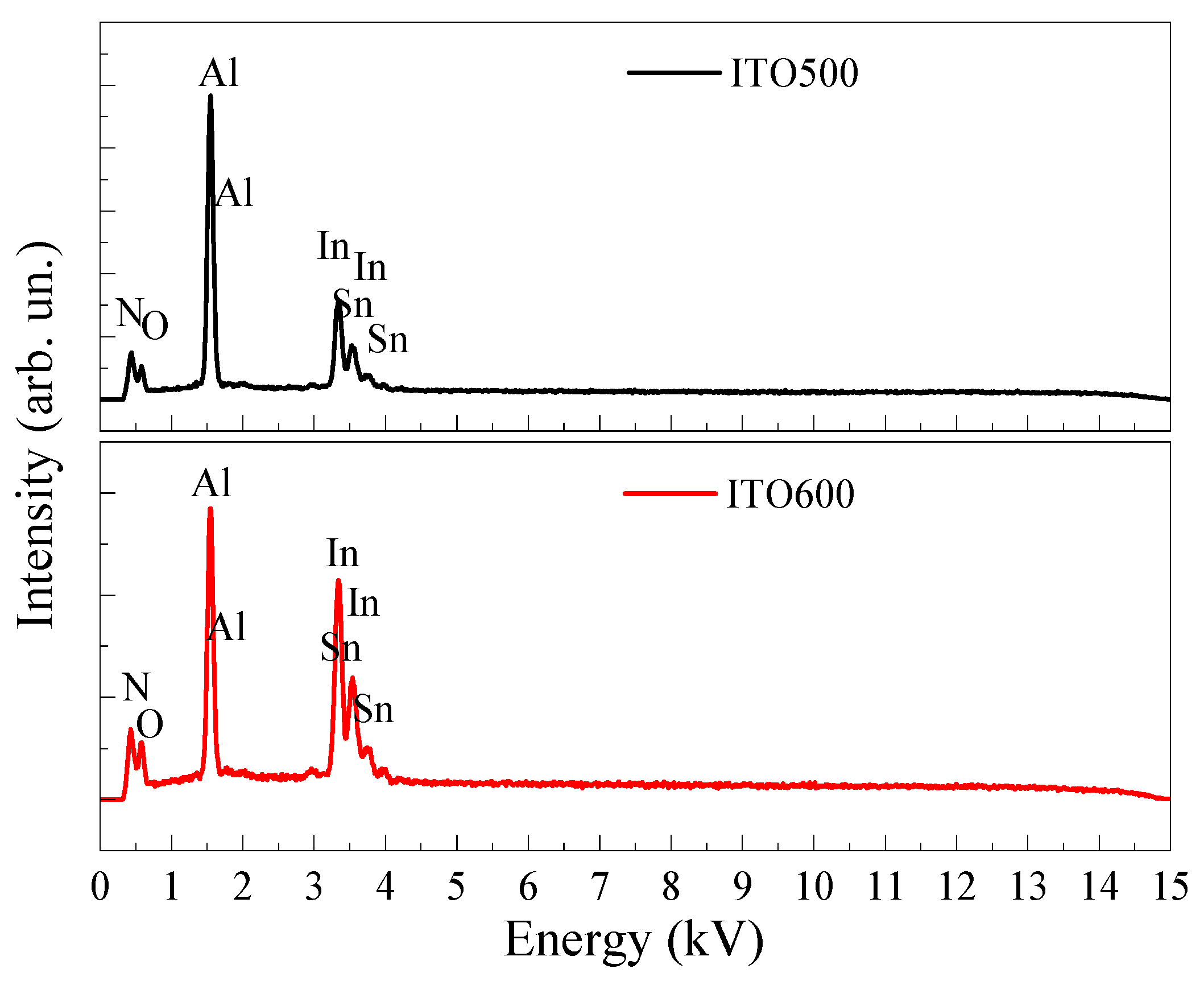
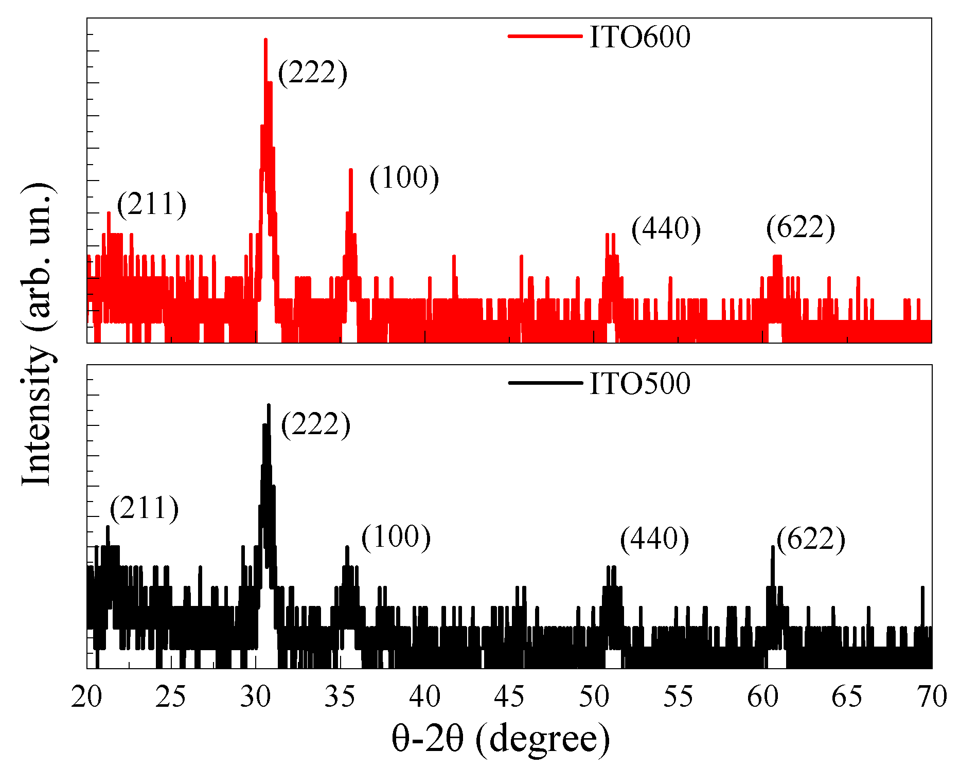
3.1. Structural Properties of ITO Thin Films

The microrelief of the ITO-500 film surface is represented by small grains with sizes of 40–100 nm, which form large agglomerates with sizes up to 350 nm (Figure 2). An increase in Tann to 600 °C leads to an increase in the size of small grains to 80–140 nm. At the same time, the sizes of agglomerates vary slightly.
The EDX spectra (Figure 3) show intense peaks of Al and N from the substrate and In, Sn and O from the film deposited on top of the substrate. An increase in Tann leads to an increase in the contents of In and Sn in the films due to a decrease in the content of O (Table 1). In Ref. [36], it was shown that in as-deposited ITO thin films, Sn forms complexes with O on the grain surface and intergrain space due to the excess of the latter. Annealing leads to the destruction of these complexes and enhances the diffusion of Sn into In2O3. The increase in grain sizes with Tann observed by AFM can lead to a decrease in the density of Sn–O complexes on the film surface.
The XRD spectra of the annealed ITO thin films are characterized by the presence of low-intensity peaks that can be associated with the (211), (222), (100), (440) and (622) crystallographic planes of the cubic In2O3 phase (Figure 4). The spectra were measured at a shallow angle. For this reason, it was not possible to detect peaks from the substrate. The content of SnO2 is not enough to detect its phase in ITO thin films using XRD. Similar XRD spectra were observed earlier for ITO thin films [25,29,30,31]. An increase in Tann leads to an increase in the intensity of the peaks without changing their position. The estimation of the crystallite sizes D using the Scherrer equation was made for the most intense peaks associated with the (222) and (100) crystallographic planes. For ITO-500 films, D = 22.6 nm and 20.9 nm, respectively, for these peaks. An increase in Tann to 600 °C leads to an increase in the D to 26.1 nm and 28.0 nm.
The optical transmission spectra of ITO films annealed at Tann = 500 °C and 600 °C are shown in Figure 5a. The transmission at wavelengths λ > 400 nm exceeds 80%, which is characteristic of ITO films [37]. In this wavelength region, the annealing temperature does not significantly affect the transmission values. The observed peak in the range of λ = 450–475 nm is caused by interference phenomena in the film–substrate system. With a decrease in λ from 400 nm to 320 nm, the transmission decreases due to the band-to-band absorption. In this λ range, the transmittance of ITO films annealed at Tann = 600 °C is slightly higher. Optical absorption spectra can be analyzed fairly accurately from the curves of α2 vs. photon energy (Figure 5b) characterized for the direct-band-gap semiconductor, where α is the absorption coefficient. The band gaps Eg were 3.62 eV and 3.65 eV for the ITO-500 and ITO-600 films, respectively. The obtained values of Eg and those indicated in Refs. [37,38] for MS-deposited ITO thin films are practically the same.
Thus, the studied films are a mixture of indium and tin oxides, with the content of the latter at a level corresponding to ITO. It will be shown below that ITO thin films are of interest for the development of low-resistance gas sensors. For this reason, in this work, we have focused on the gas-sensitive properties of the material. In the future, we plan to conduct detailed studies of the structural properties of ITO thin films by means of X-ray photoelectron and Raman spectroscopies, just as was implemented in Refs. [39,40].

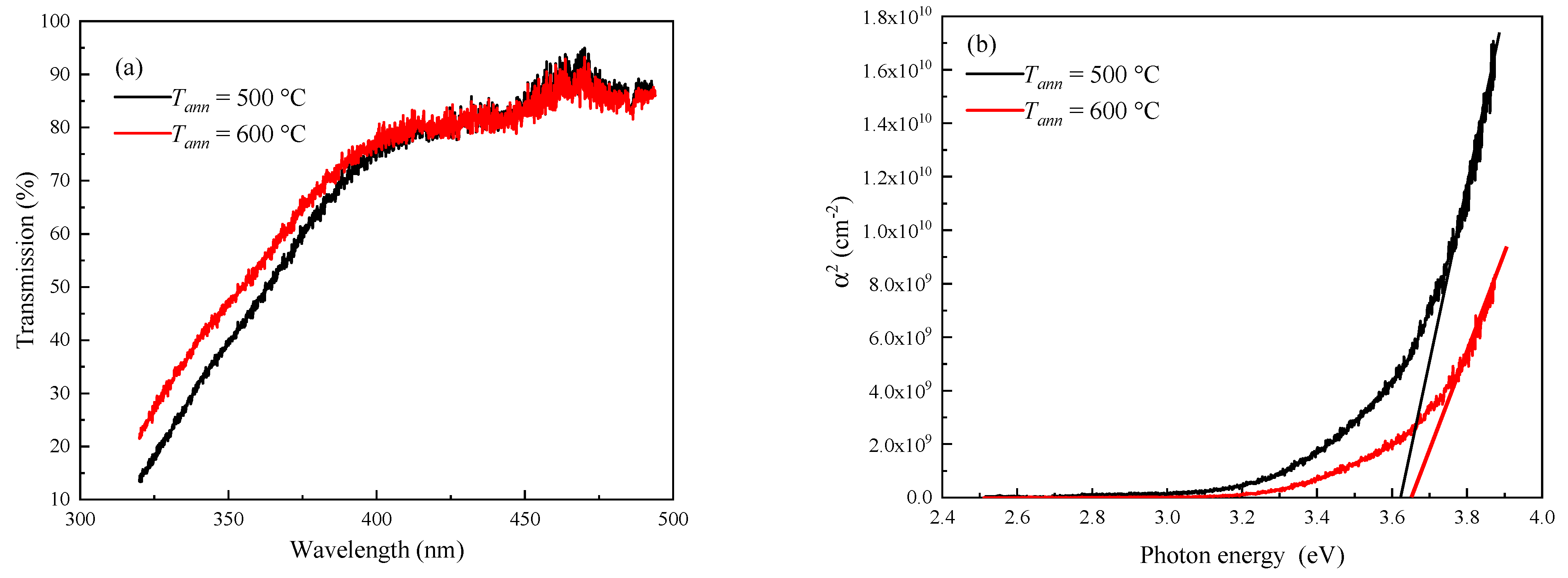
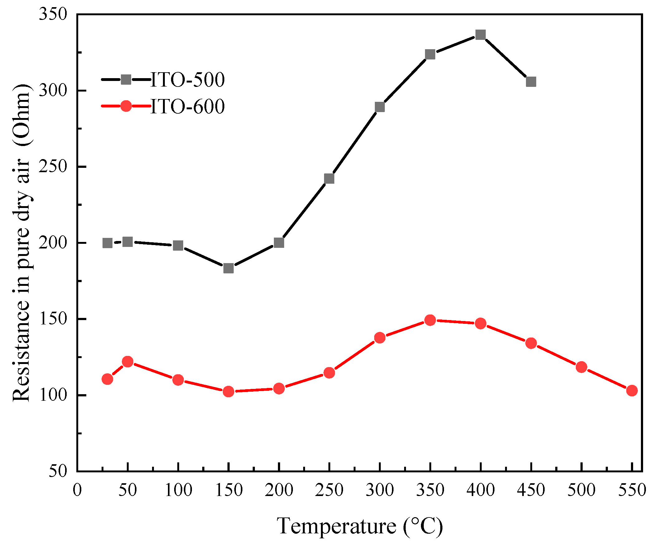
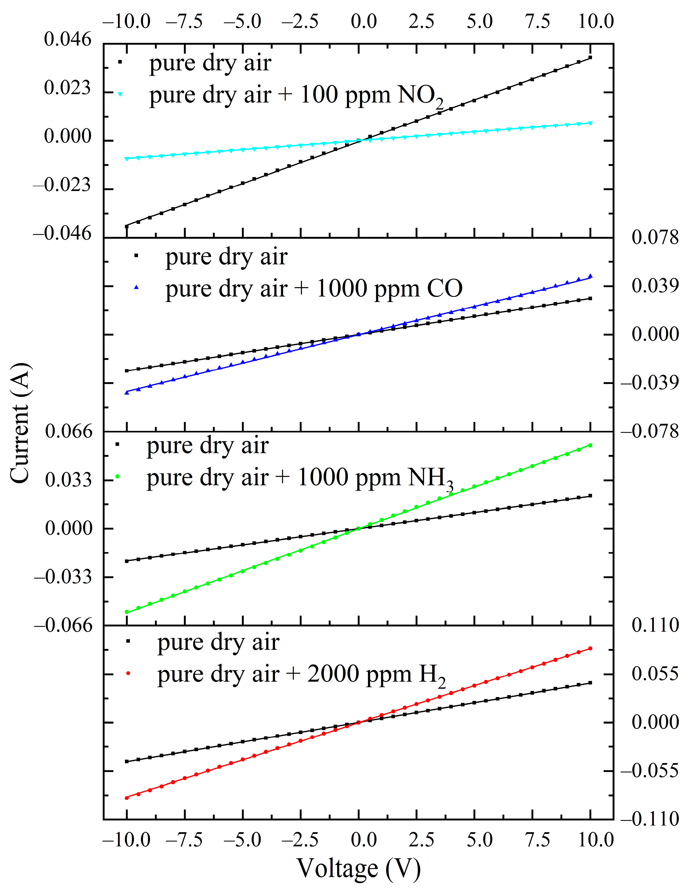
3.2. The Electrically Conductive Properties of ITO Thin Films in Pure Dry Air

Figure 6 shows the temperature dependence of the ITO thin-film resistance in pure dry air, Rair. Rair decreases slightly with an increase in T in the range from 50 °C to 150 °C regardless of Tann, which is characteristic of a semiconductor. Rair increases with a further increase in T to 350–400 °C. The active chemisorption of oxygen on the thin-film surface and the transition of chemisorbed oxygen from the molecular form O2 to atomic O take place in this T range [20,21,22]. The atomic form of chemisorbed oxygen is the most active in interacting with reducing gases. An increase in resistance with T is characteristic of thin films. The surface determines the electrically conductive properties to a greater extent than the bulk of thin films. During chemisorption, oxygen captures electrons from the conduction band of a semiconductor [20,21,22]. Increasing T from 200 °C to 350–400 °C leads to a rise in Ni and a drop in the electron concentration n in the film. At T > 350–400 °C, the desorption of O manifests, and Rair drops again with temperature. The observed increase in Rair correlates with the results of Hall measurements for polycrystalline ITO thin films [41]. Electron mobility decreases slightly with T due to ionized impurity scattering and grain boundary scattering. The electron concentration in the T range from 25 °C to 200 °C does not significantly change and significantly decreases with an increase in T to 500 °C. The decrease in n is due to the interaction of the ITO film with oxygen.
An increase in Tann of ITO thin films leads to a decrease in Rair, mainly due to the observed increase in grain size [42]. It was shown in Refs. [36,43] that an increase in the grain size of ITO thin films with Tann leads to a decrease in film resistance due to an increase in carrier mobility. Increasing the grain size of the studied ITO thin films was confirmed by our results of ASM and XRD. The ITO thin-film resistance at different temperatures does not exceed 350–400 Ohms. Thus, sensors based on the studied films have low nominal resistance.

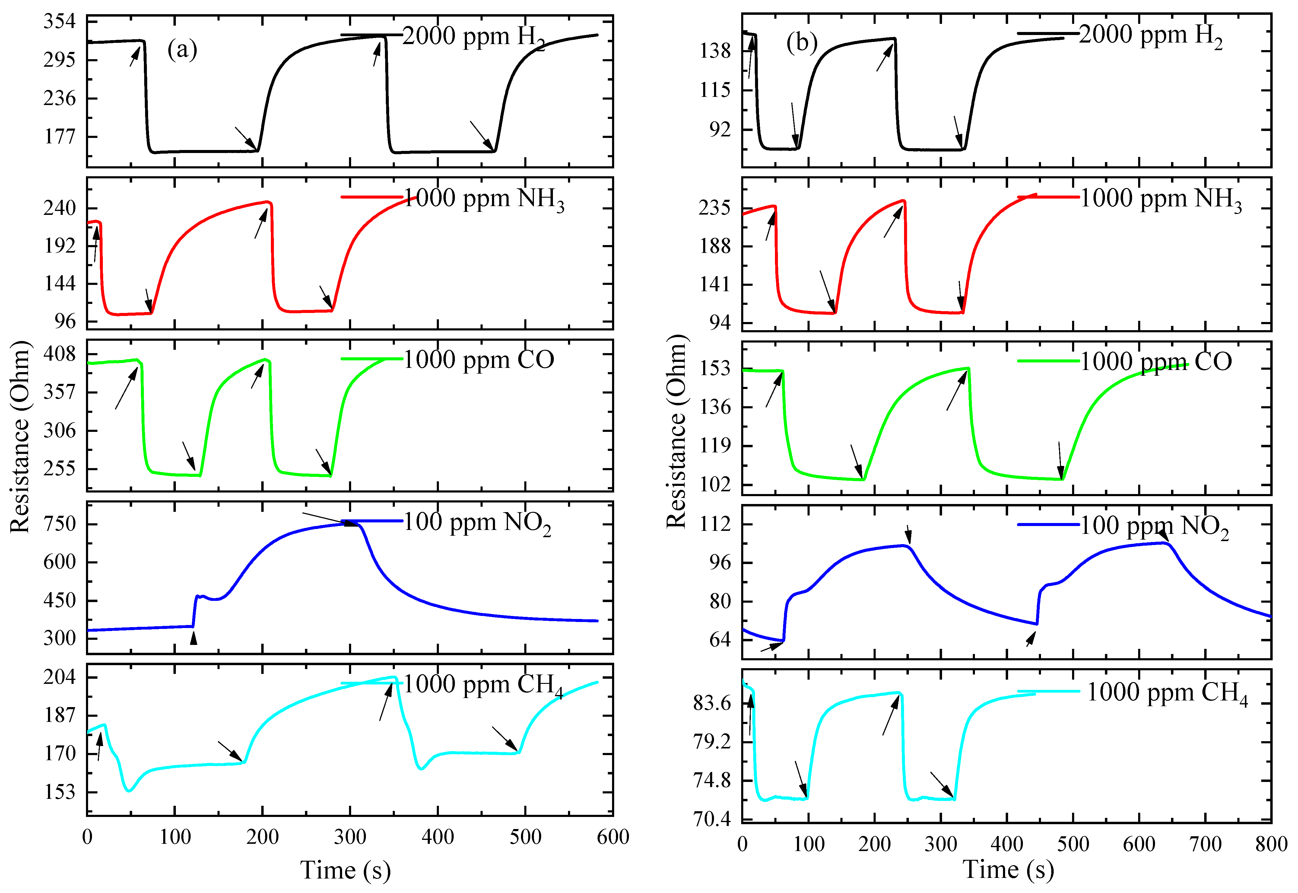
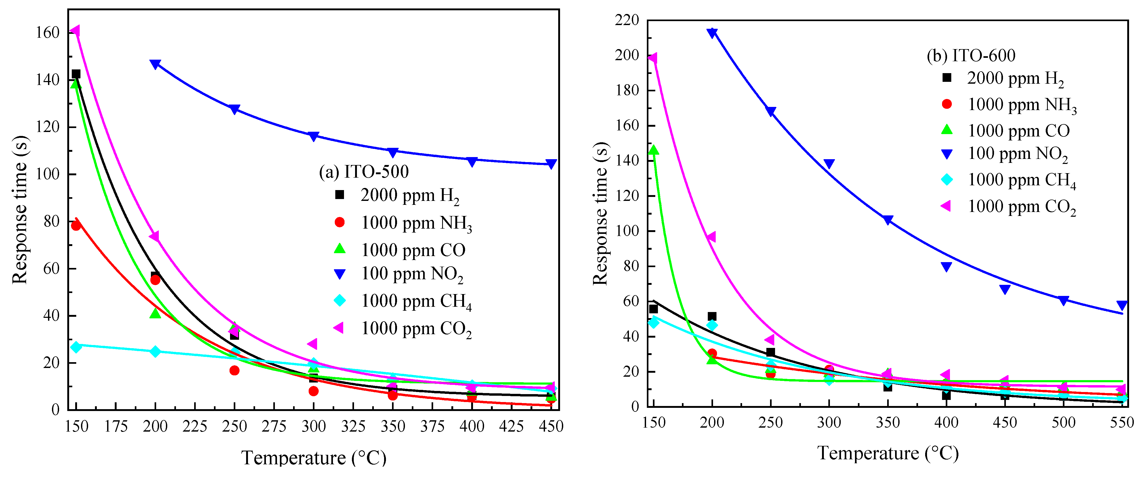
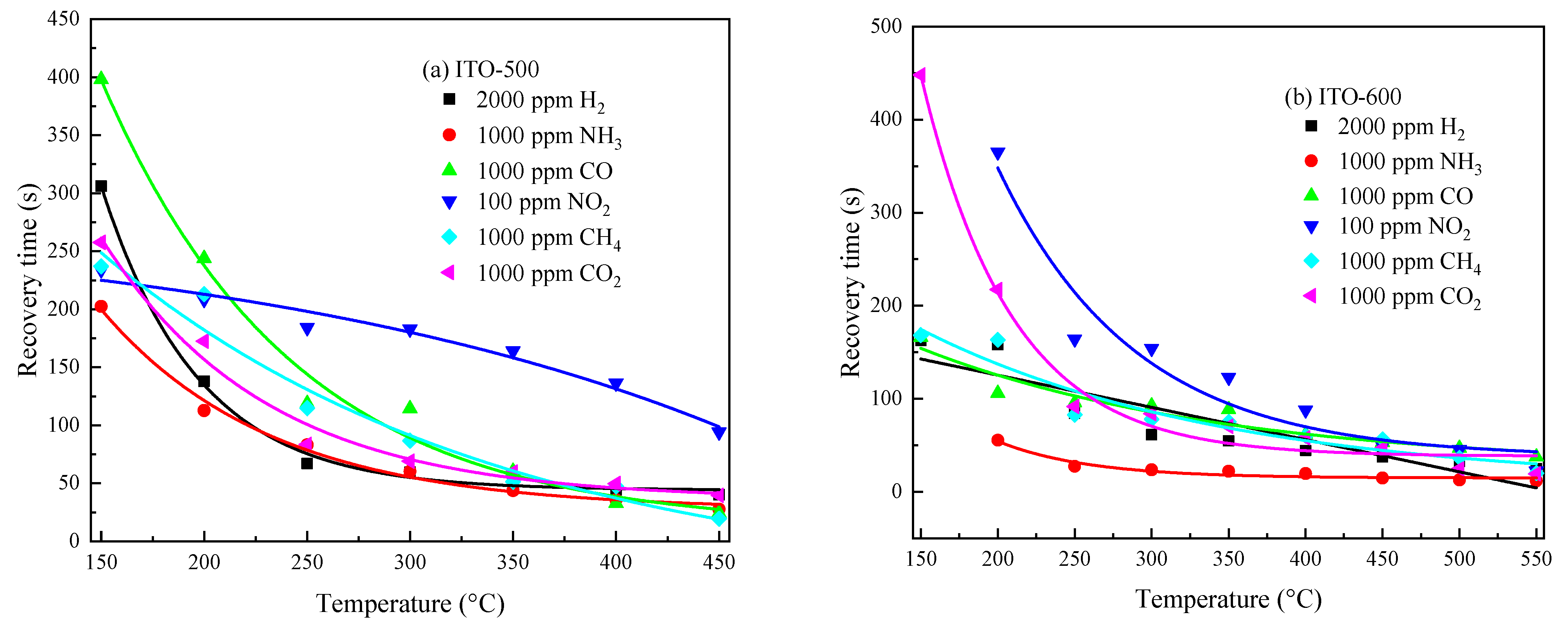
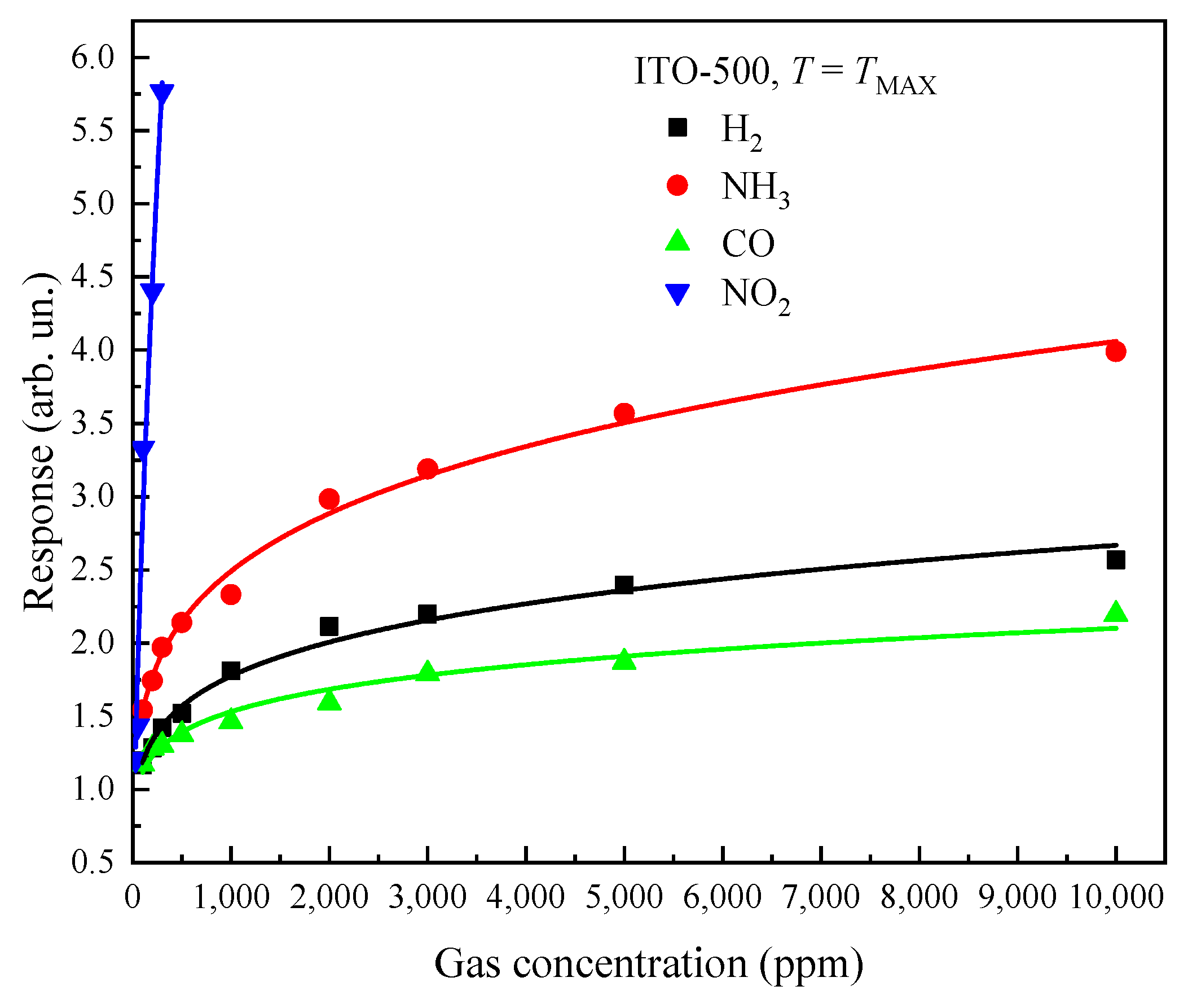
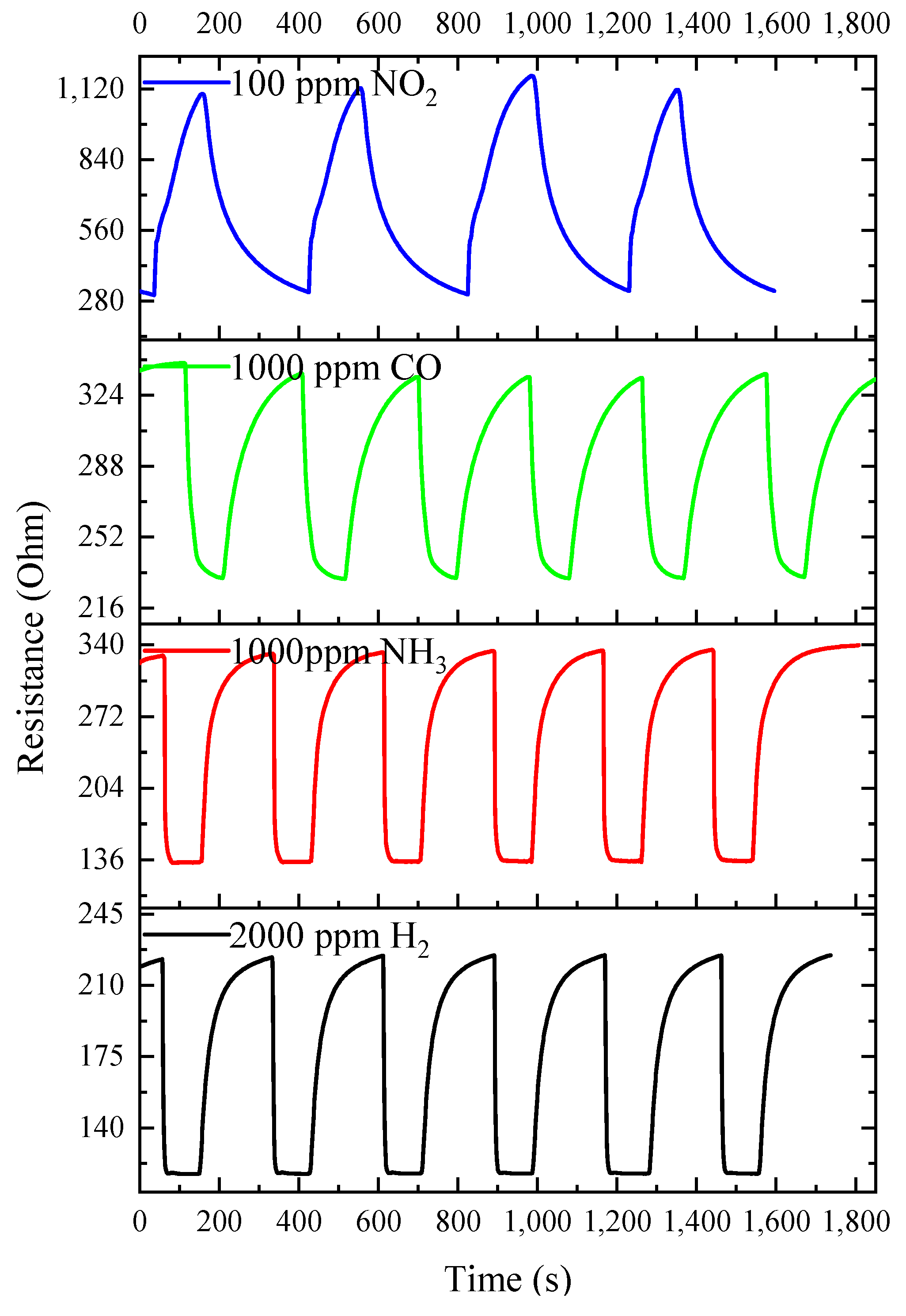
3.3. Gas-Sensitive Properties of ITO Thin Films

Figure 7 shows the dependence of the responses to fixed concentrations of various gases on the temperature for ITO thin films annealed at Tann = 500 °C and 600 °C. Exposure to the reducing gases H2, NH3, CO and CH4 in the temperature ranges of 150–450 °C and 150–550 °C for ITO-500 and ITO-600 thin films, respectively, leads to a reversible decrease in their resistance. In the region of low temperatures, T ≤ 100 °C, the resistance of the samples after their exposure to the gases is practically unrecovered. The following relation was selected for the response to reducing gases:
S1 = Rair/Rg,
where Rg is the ITO thin-film resistance in a gas mixture of pure dry air + target gas (H2, NH3, CO and CH4). The exposure to NO2 leads to a reversible increase in ITO thin-film resistance. The following relation was used for the response to NO2:
S2 = RNO2/Rair,
where RNO2 is the ITO thin-film resistance in a gas mixture of pure dry air + NO2. The curves in Figure 7 are characterized by the presence of maxima SMAX at a certain temperature, TMAX. It is advisable to choose TMAX as the operating temperature. TMAX and SMAX for various gases for ITO thin films annealed at Tann = 500 °C and 600 °C are presented in Table 2, where ng is the target gas concentration. The highest responses to NH3 and NO2 are observed for ITO-500 thin films. An increase in Tann leads to a decrease in the responses of ITO thin films to all gases except NH3. ITO thin films exhibit relatively low responses to CH4. Table 2 also shows the resistance in pure air at T = TMAX. The observed variations in Rair are due to variations in the tin concentration in the ITO thin films (Table 1).
The time dependence of the ITO thin-film resistance at Tann = 500 °C and 600 °C under exposure to various gases at T = TMAX is shown in Figure 8. The falling and rising regions of the ITO thin-film resistance under exposure to reducing gases are approximated by the following functions, respectively:
R(t) = Rg + A1exp[−t1],
R(t) = RairB2exp[−t2],
where A1 and B2 are constants; t is time; and τ1 and τ2 are time constants for the falling and rising regions of the ITO thin-film resistance under exposure to reducing gases. The rising region of ITO thin-film resistance under exposure to NO2 is approximated by the function:
R(t) = RNO2ANO2exp[−t3],
and the falling-region resistance after exposure to NO2 is approximated by the function:
R(t) = Rair + BNO2exp[−t4],
where ANO2 and BNO2 are constants; τ3 and τ4 are time constants for the rising and falling regions of the ITO thin-film resistance under exposure to NO2.
τ1, τ3 and τ2, τ4 are defined by the relaxation times τ of the adsorption/desorption processes of gas molecules on the semiconductor surface: τ ~ exp[(ED–EA)/(2kT)] [44], where EA and ED are the activation energies of the adsorption and desorption of gas molecules on the semiconductor surface, respectively; k is the Boltzmann constant. τ and, consequently, τ1, τ3 and τ2, τ4 decrease sharply with T. It can be seen from Expressions (3) and (4) that at t ≥ 2.3τ1 and t ≥ 2.3τ2, stationary values of Rg and Rair are achieved. The response time tres = 2.3τ1 and the recovery time trec = 2.3τ2 can be used to evaluate the operation speed of ITO thin films under exposure to reducing gases. tres = 2.3τ3 and trec = 2.3τ4 under exposure to NO2. The temperature dependence of the response and recovery times for ITO thin films is shown in Figure 9 and Figure 10, respectively.
The response and recovery times drop exponentially with T. The response times of ITO thin films for all reducing gases at T ≥ 350 °C do not exceed 20 s, and the recovery times do not exceed 100 s. The longest tres and trec are observed under exposure to NO2, which is caused by the large value of the binding energy of this molecule to the surface [45].
ITO thin films annealed at Tann = 500 °C are characterized by the highest responses to H2, NH3, CO and NO2. Therefore, only these films will be further considered. Figure 11 shows the dependence of the responses on H2, NH3, CO and NO2 concentrations for ITO-500 thin films at T = TMAX. The response increases with the concentration according to the power law, S1,2 ~ ngm, where m is the power index. The m values for H2, NH3, CO and NO2 at T = TMAX are compared in Table 3.
Figure 12 shows the time dependence of the resistance of ITO-500 thin films at T = TMAX and under cyclic exposure to H2, NH3, CO and NO2. Estimates have shown that the drift of ITO-500 thin-film characteristics is practically absent under exposure to reducing gases. The deviations of Rair, Rg and S1 from the average values do not exceed 1%. Significant deviations of 5% occurred under exposure to NO2. The IV characteristics of ITO-500 films in pure dry air and when exposed to H2, NH3, CO and NO2 are linear in the voltage range of −10–10 V (Figure 13). Exposure to gases leads to a change in the slope of the IV characteristics due to a change in the ITO thin-film resistance.
Estimates have shown that LD for ITO-500 thin films increases from 0.57 nm to 1.1 nm with an increase in T from 30 °C to 450 °C. Thus, the ratio Dg >> LD was obtained, and an over-barrier conduction mechanism is manifested for ITO-500 thin films. In this case, the conductivity G of the thin film is as follows [20,21,22]:
G(T) = G00(T)exp[eφs(T)/(kT)],
where G00 is a parameter that weakly depends on changes in the atmospheric composition and is determined by the geometric dimensions of the ITO film and its electrophysical characteristics; eφs is the band-bending energy at the grain boundaries; φs is the surface potential; and e is the electron charge. In an atmosphere of air, oxygen molecules are chemisorbed on the surface of the semiconductor.
For an n-type semiconductor, oxygen chemisorption leads to the upward bending of energy bands [20,21,22]. The predominant form of chemisorbed oxygen in the range of T = 150–500 °C is O [46]. For metal oxide semiconductors, eφs ~ Ni2 and eφs ~ nO2l, where nO2 is the oxygen concentration in the gas mixture; l is an index that depends on the adsorption properties of the semiconductor surface, adsorption centers, etc., with l < 1. Under exposure to reducing gases, the interaction between their molecules and previously chemisorbed O- ions takes place, leading to decreases in Ni and eφs. NO2 molecules are able to chemisorb onto free adsorption centers and, like oxygen, capture electrons from the conduction band of the semiconductor. This process leads to an additional increase in eφs ~ (Ni + NNO2)2, where NNO2 is the surface density of chemisorbed NO2. Changes in G when exposed to gases are caused mainly by changes in eφs. Interactions between target gas molecules and O on the ITO surface can be described by the following reactions [47,48,49]:
H2 + O → H2O + e,
2NH3 + 3O → N2 + 3H2O + 3e,
CH4 + 4O → CO2 + 2H2O + 4e,
CO + O → CO2 + e.
NO2 + e → NO2,
As a result of Reactions (8)–(11), the conductivity of the semiconductor increases, and reaction products in the form of H2O, N2 and CO2 molecules are desorbed. Reactions (8)–(12) are the simplest possible and only fundamentally explain the observed sensory effect. Many reasonable variants of other reactions on the surface of metal oxide semiconductors have been proposed. Their consideration is not advisable to describe a qualitative model of the sensory effect for the studied ITO films.
In Ref. [26], the sensory mechanism of the In2O3 and SnO2 mixed-oxide system was studied in more detail. The tin oxide content in the mixture varied widely. It was found that with an increase in the content of SnO2 from 0 to 10 wt.%, the conductivity of the mixture increases, and the response to H2 decreases. This composition corresponds to the studied ITO thin film. The limit of SnO2 solubility in In2O3 is 10–15 wt.%. The electrically conductive and gas-sensitive properties of the In2O3 and SnO2 mixed-oxide system are determined by In2O3 up to these values of SnO2 concentration. The introduction of Sn into the In2O3 matrix leads to a decrease in the surface density of chemisorbed oxygen ions and the responses of the films to H2. With a further increase in the concentration of SnO2, the conductivity decreases, and the response to H2 increases. Thus, in our case, Sn (SnO2) acts as an additive to In2O3 and reduces the resistance of the film. The sensing properties of the studied ITO thin films are determined by In2O3.
Table 4 shows a comparison of the gas-sensitive characteristics of ITO thin films with a SnO2 content of 5–10%. The resistance Rair and resistivity ρair of ITO thin films in pure air were measured at room temperature. It is worth noting that for most ITO thin films, high responses to gases corresponded to high nominal resistance. As a rule, high-sensitivity ITO films are characterized by a low thickness, less than 90 nm. High responses were shown by ITO films with an island microstructure [28]. The diameter of the ITO islands was several tens of nanometers. Depositing ultra-thin continuous and homogeneous semiconductor films by means of the MS method is a difficult task due to its peculiarities [50]. Nevertheless, reducing the film thickness is a promising method for enhancing gas sensitivity. The resistance and response to gases of the ITO films are significantly reduced at the high thickness of 300 nm [31]. The main advantage of the studied ITO thin films is the possibility of developing sensors with low nominal resistance (Rair) and relatively high sensitivity to gases (H2, NH3 and NO2).

4. Conclusions

The structural, optical, electrically conductive and gas-sensitive properties of magnetron-sputtered ITO thin films on AlN ceramic substrates annealed in air for 60 min at temperatures of 500 °C and 600 °C were investigated. The microrelief of ITO films annealed at 500 °C was represented by grains with dimensions of 40–100 nm, which form agglomerates up to 350 nm in size. The tin content in these films was 4.10–5.15 wt.%, and the band-gap energy was 3.62 eV. An increase in the annealing temperature to 600 °C led to increases in the size of grains to 80–140 nm, in the tin content to 4.97–6.15 wt.%, and in the band-gap energy to 3.65 eV. In pure dry air, the ITO thin-film resistance annealed at 500 °C does not exceed 350 Ohms, and the resistance of films annealed at 600 °C dropped by about 2 times. Sensitivity to H2, NH3, CO, NO2 and CH4 was studied in the operating temperature ranges of 150–450 °C and 150–550 °C for ITO films annealed at 500 °C and 600 °C, respectively. ITO films annealed at 500 °C were characterized by higher sensitivity to gases. The maximum responses to 2000 ppm H2, 1000 ppm NH3 and 100 ppm NO2 for these films were 2.21, 2.39 and 2.14 at operating temperatures of 400 °C, 350 °C and 350 °C, respectively. An increase in the annealing temperature led to a decrease in the gas sensitivity of the films. At operating temperatures of at least 350 °C, the films were characterized by short response and recovery times that did not exceed 20 s and 100 s, respectively, under exposure to reducing gases. The drift of the ITO film characteristics under cyclic exposure to reducing gases did not exceed 1%. A qualitative model of the sensory effect was proposed. The gas sensitivity of the ITO films was determined mainly by In2O3. SnO2 acted only as an additive, a source of Sn donor impurities. The possibility of developing sensors with low nominal resistance and relatively high sensitivity to gases was shown.

Author Contributions

Conceptualization, A.V.A., A.B.U. and A.I.P.; methodology, A.V.A., V.V.K. and Z.T.K.; software, V.V.K.; validation, A.V.A.; formal analysis, A.V.A. and A.T.A.; investigation, A.V.A., V.V.K., V.A.N., A.V.C., Z.K.K. and N.N.Y.; resources, A.V.A.; data curation, A.V.A., V.V.K., V.A.N. and A.V.C.; writing—original draft preparation, A.V.A. and N.N.Y.; writing—review and editing, A.V.A. and A.B.U.; visualization, A.V.A.; supervision, A.V.A.; project administration, A.V.A. and A.B.U.; funding acquisition, A.V.A. and A.B.U. All authors have read and agreed to the published version of the manuscript.

Funding

This research was funded by the Science Committee of the Ministry of Education and Science of the Republic of Kazakhstan (Grant No. AP08856540). The research was carried out with the support of a grant under the Decree of the Government of the Russian Federation No. 220 of 9 April 2010 (Agreement No. 075-15-2022-1132 of 1 July 2022). In addition, this research was partly performed at the Institute of Solid State Physics, University of Latvia (ISSP UL). ISSP UL, as the Centre of Excellence, has received funding from the European Union’s Horizon 2020 Framework Programme H2020-WIDESPREAD01-2016-2017-Teaming Phase2 under Grant Agreement No. 739508, project CAMART2.

Institutional Review Board Statement

Not applicable.

Informed Consent Statement

Not applicable.

Data Availability Statement

Not applicable.

Conflicts of Interest

The authors declare no conflict of interest.

References

  1. Korotcenkov, G. Metal oxides for solid-state gas sensors: What determines our choice? Mater. Sci. Eng. B 2007, 139, 1–23. [Google Scholar] [CrossRef]
  2. Shah, V.; Bhaliya, J.; Patel, G.M.; Joshi, P. Room-Temperature Chemiresistive Gas Sensing of SnO2 Nanowires: A Review. J. Inorg. Organomet. Polym. 2022, 32, 741–772. [Google Scholar] [CrossRef]
  3. Afzal, A. β-Ga2O3 nanowires and thin films for metal oxide semiconductor gas sensors: Sensing mechanisms and performance enhancement strategies. J. Mater. 2019, 5, 542–557. [Google Scholar] [CrossRef]
  4. Gu, H.; Wang, Z.; Hu, Y. Hydrogen Gas Sensors Based on Semiconductor Oxide Nanostructures. Sensors 2012, 12, 5517–5550. [Google Scholar] [CrossRef] [Green Version]
  5. Shi, Y.; Xu, H.; Liu, T.; Zeb, S.; Nie, Y.; Zhao, Y.; Qin, C.; Jiang, X. Advanced development of metal oxide nanomaterials for H2 gas sensing applications. Mater. Adv. 2021, 2, 1530. [Google Scholar] [CrossRef]
  6. Koo, W.-T.; Cho, H.-J.; Kim, D.-H.; Kim, Y.H.; Shin, H.; Penner, R.M.; Kim, I.D. Chemiresistive Hydrogen Sensors: Fundamentals, Recent Advances, and Challenges. ACS Nano 2020, 14, 14284–14322. [Google Scholar] [CrossRef]
  7. Padvi, M.N.; Moholkar, A.V.; Prasad, S.R.; Prasad, N.R. A Critical Review on Design and Development of Gas Sensing Materials. Eng. Sci. 2021, 15, 20–37. [Google Scholar] [CrossRef]
  8. Comini, E. Metal oxides nanowires chemical/gas sensors: Recent advances. Mater. Today Adv. 2020, 7, 100099. [Google Scholar] [CrossRef]
  9. Grassi, M.; Malcovati, P.; Baschirotto, A. Fundamental Limitations in Resistive Wide-Range Gas-Sensor Interface Circuits Design. In Sensors and Microsystems. Lecture Notes in Electrical Engineering; Springer: Dordrecht, The Netherlands, 2010; pp. 25–29. [Google Scholar]
  10. Jang, H.; Kim, M.; Kim, Y. Batch-processed semiconductor gas sensor array for the selective detection of NOx in automotive exhaust gas. Micro Nano Syst. Lett. 2016, 4, 6. [Google Scholar] [CrossRef] [Green Version]
  11. Merino, J.L.; Bota, S.A.; Casanova, R.; Diéguez, A.; Cané, C.; Samitier, J. A Reusable Smart Interface for Gas Sensor Resistance Measurement. IEEE Trans. Instrum. Meas. 2004, 53, 1173–1178. [Google Scholar] [CrossRef]
  12. Grassi, M.; Malcovati, P.; Baschirotto, A. Wide-range integrated gas sensor interface based on a resistance-to-number converter technique with the oscillator decoupled from the input device. In Proceedings of the IEEE International Symposium on Circuits and Systems, Island of Kos, Greece, 21–24 May 2006. [Google Scholar]
  13. Barrettino, D.; Graf, M.; Taschini, S.; Hafizovic, S.; Hagleitner, C.; Hierlemann, A. CMOS Monolithic Metal–Oxide Gas Sensor Microsystems. IEEE Sens. J. 2006, 6, 276–286. [Google Scholar] [CrossRef]
  14. Figaro USA, Inc. Available online: https://www.figarosensor.com/ (accessed on 30 October 2022).
  15. Moumen, A.; Kumarage, G.C.W.; Comini, E. P-Type Metal Oxide Semiconductor Thin Films: Synthesis and Chemical Sensor Applications. Sensors 2022, 22, 1359. [Google Scholar] [CrossRef] [PubMed]
  16. Fleischer, M.; Meixner, H. Thin-film gas sensors based on high-temperature-operated metal oxides. J. Vac. Sci. Technol. A 1991, 17, 1866. [Google Scholar] [CrossRef]
  17. Soonmin, H.; Vanalakar, S.A.; Galal, A.; Singh, V.N. A review of nanostructured thin films for gas sensing and corrosion protection. Mediterr. J. Chem. 2019, 7, 433–451. [Google Scholar] [CrossRef]
  18. Rydosz, A.; Brudnik, A.; Staszek, K. Metal Oxide Thin Films Prepared by Magnetron Sputtering Technology for Volatile Organic Compound Detection in the Microwave Frequency Range. Materials 2019, 12, 877. [Google Scholar] [CrossRef] [Green Version]
  19. Maksimova, N.K.; Almaev, A.V.; Sevastyanov, E.Y.; Potekaev, A.I.; Chernikov, E.V.; Sergeychenko, N.V.; Korusenko, P.M.; Nesov, S.N. Effect of Additives Ag and Rare-Earth Elements Y and Sc on the Properties of Hydrogen Sensors Based on Thin SnO2 Films during Long-Term Testing. Coatings 2019, 9, 423. [Google Scholar] [CrossRef] [Green Version]
  20. Gaman, V.I. Basic physics of semiconductor hydrogen sensors. Russ. Phys. J. 2008, 51, 425–441. [Google Scholar] [CrossRef]
  21. Sahm, T.; Gurlo, A.; Bârsan, N.; Weimar, U.; Mädler, L. Fundamental studies on SnO2 by means of simultaneous work function change and conduction measurements. Thin Solid Films 2005, 490, 43–47. [Google Scholar] [CrossRef]
  22. Yamazoe, N.; Shimanoe, K. Receptor Function and Response of Semiconductor Gas Sensor. J. Sens. 2009, 2009, 875704. [Google Scholar] [CrossRef]
  23. Korotcenkov, G.; Cho, B.K. Engineering approaches to improvement of conductometric gas sensor parameters. Part 2: Decrease of dissipated (consumable) power and improvement stability and reliability. Sens. Actuators B Chem. 2014, 198, 316–341. [Google Scholar] [CrossRef]
  24. Zappa, D.; Galstyan, V.; Kaur, N.; Sisman, O.; Comini, E. Metal oxide -based heterostructures for gas sensors—A review. Anal. Chim. Acta 2018, 1, 1039. [Google Scholar] [CrossRef] [PubMed]
  25. Mokrushin, A.S.; Fisenko, N.A.; Gorobtsov, P.Y.; Simonenko, T.L.; Glumov, O.V.; Melnikova, N.A.; Simonenko, N.P.; Bukunov, K.A.; Simonenko, E.P.; Sevastyanov, V.G.; et al. Pen plotter printing of ITO thin film as a highly CO sensitive component of a resistive gas sensor. Talanta 2021, 221, 121455. [Google Scholar] [CrossRef] [PubMed]
  26. Gerasimov, G.N.; Gromov, V.F.; Ikim, M.I.; Ilegbusi, O.J.; Ozerin, S.A.; Trakhtenberg, L.I. Structure and gas-sensing properties of SnO2-In2O3 nanocomposites synthesized by impregnation method. Sens. Actuators B Chem. 2020, 320, 128406. [Google Scholar] [CrossRef]
  27. Lin, C.-W.; Chen, H.-I.; Chen, T.-Y.; Huang, C.-C.; Hsu, C.-S.; Liu, R.-C.; Liu, W.-C. On an indium–tin-oxide thin film based ammonia gas sensor. Sens. Actuators B Chem. 2011, 160, 1481–1484. [Google Scholar] [CrossRef]
  28. Yang, M.; Hong, S.H. Orientation and thickness dependence of electrical and gas sensing properties in heteroepitaxial indium tin oxide films. Sens. Actuators B Chem. 2011, 160, 490–498. [Google Scholar] [CrossRef]
  29. Lin, C.-W.; Chen, H.-I.; Chen, T.-Y.; Huang, C.-C.; Hsu, C.-S.; Liu, W.-C. Ammonia Sensing Characteristics of Sputtered Indium Tin Oxide (ITO) Thin Films on Quartz and Sapphire Substrates. IEEE Trans. Electron Devices 2011, 58, 4407–4412. [Google Scholar] [CrossRef]
  30. Yang, M.; Hong, S.-H. Fabrication of ITO / SnO2 Two-Layer Thin Films and Their Gas Sensing Properties. J. Electrochem. Soc. 2010, 157, J392. [Google Scholar] [CrossRef]
  31. Murali, A.; Sohn, H.Y. Plasma-assisted chemical vapor synthesis of indium tin oxide (ITO) nanopowder and hydrogen-sensing property of ITO thin film. Mater. Res. Express 2018, 5, 065045. [Google Scholar] [CrossRef]
  32. Nicolescu, M.; Mitrea, D.; Hornoiu, C.; Preda, S.; Stroescu, H.; Anastasescu, M.; Calderon-Moreno, J.M.; Predoana, L.; Teodorescu, V.S.; Maraloiu, V.-A.; et al. Structural, Optical, and Sensing Properties of Nb-Doped ITO Thin Films Deposited by the Sol–Gel Method. Gels 2022, 8, 717. [Google Scholar] [CrossRef]
  33. Lopez-Santos, C.; Puerto, D.; Siegel, J.; Macias-Montero, M.; Florian, C.; Gil-Rostra, J.; López-Flores, V.; Borras, A.; González-Elipe, A.R.; Solis, J. Anisotropic Resistivity Surfaces Produced in ITO Films by Laser-Induced Nanoscale Self-organization. Adv. Opt. Mater. 2021, 9, 2001086. [Google Scholar] [CrossRef]
  34. Thirumoorthi, M.; Thomas Joseph Prakash, J. Structure, optical and electrical properties of indium tin oxide ultra thin films prepared by jet nebulizer spray pyrolysis technique. J. Asian Ceram. Soc. 2016, 4, 124–132. [Google Scholar] [CrossRef] [Green Version]
  35. Jafan, M.-H.; Zamani-Meymian, M.-R.; Rahimi, R.; Rabbani, M. The effect of solvents and the thickness on structural, optical and electrical properties of ITO thin films prepared by a sol–gel spin-coating process. J. Nanostruct. Chem. 2014, 4, 89. [Google Scholar] [CrossRef] [Green Version]
  36. Wu, W.F.; Chiou, B.-S. Effect of annealing on electrical and optical properties of RF magnetron sputtered indium tin oxide films. Appl. Surf. Sci. 1993, 68, 497–504. [Google Scholar] [CrossRef]
  37. Krylov, P.N.; Zakirova, R.M.; Fedotova, I.V. Optical properties of ITO films obtained by high-frequency magnetron sputtering with accompanying ion treatment. Semiconductors 2013, 47, 1412–1415. [Google Scholar] [CrossRef]
  38. Bochenkov, V.E.; Sergeev, G.B. Adsorption, catalysis, and reactions on the surfaces of metal nano-oxides. Catal. Ind. 2010, 2, 1–10. [Google Scholar] [CrossRef]
  39. Hernández-Gutiérrez, C.A.; Kudriavtsev, Y.; Cardona, D.; Hernández, A.G.; Camas-Anzueto, J.L. Optical, electrical, and chemical characterization of nanostructured InxGa1-xN formed by high fluence In+ ion implantation into GaN. Opt. Mat. 2021, 111, 110541. [Google Scholar] [CrossRef]
  40. Hernández-Gutiérrez, C.A.; Casallas-Moreno, Y.L.; Rangel-Kuoppa, V.-T.; Cardona, D.; Hu, Y.; Kudriavtsev, Y.; Zambrano-Serrano, M.A.; Gallardo-Hernandez, S.; Lopez-Lopez, M. Study of the heavily p-type doping of cubic GaN with Mg. Sci. Rep. 2020, 10, 16858. [Google Scholar] [CrossRef]
  41. Hohmann, M.V.; Wachau, A.; Klein, A. In situ Hall effect and conductivity measurements of ITO thin films. Solid State Ionics 2014, 262, 636–639. [Google Scholar] [CrossRef]
  42. Hamzah, N.A.; Asri, R.I.M.; Ahmad, M.A.; Md Sahar, M.A.A.Z.; Waheeda, S.N.; Hassan, Z. Effect of post-annealing in oxygen environment on ITO thin films deposited using RF magnetron sputtering. J. Phys. Conf. Ser. 2020, 1535, 012036. [Google Scholar] [CrossRef]
  43. Korotcenkov, G.; Brinzari, V.; Golovanov, V.; Blinov, Y. Kinetics of gas response to reducing gases of SnO2 films, deposited by spray pyrolysis. Sens. Actuators B Chem. 2004, 98, 41–45. [Google Scholar] [CrossRef]
  44. Almaev, A.V.; Yakovlev, N.N.; Chernikov, E.V.; Tolbanov, O.P. Selective Sensors of Nitrogen Dioxide Based on Thin Tungsten Oxide Films under Optical Irradiation. Tech. Phys. Lett. 2019, 45, 1016–1019. [Google Scholar] [CrossRef]
  45. Gurlo, A. Interplay between O2 and SnO2: Oxygen Ionosorption and Spectroscopic Evidence for Adsorbed Oxygen. ChemPhysChem 2006, 7, 2041–2052. [Google Scholar] [CrossRef] [PubMed]
  46. Forleo, A.; Francioso, L.; Capone, S.; Casino, F.; Siciliano, P.; Tan, O.K.; Hui, H. Fabrication at wafer level of miniaturized gas sensors based on SnO2 nanorods deposited by PECVD and gas sensing characteristics. Sens. Actuators B Chem. 2011, 154, 283–287. [Google Scholar] [CrossRef]
  47. Vorobyeva, N.; Rumyantseva, M.; Platonov, V.; Filatova, D.; Chizhov, A.; Marikutsa, A.; Bozhev, I.; Gaskov, A. Ga2O3(Sn) Oxides for High-Temperature Gas Sensors. Nanomaterials 2021, 11, 2938. [Google Scholar] [CrossRef] [PubMed]
  48. Basu, S.; Basu, P.K. Nanocrystalline Metal Oxides for Methane Sensors: Role of Noble Metals. J. Sens. 2009, 2009, 861968. [Google Scholar] [CrossRef]
  49. Jiao, Z.; Wu, M.; Qin, Z.; Lu, M.; Gu, J. The NO2 sensing ITO thin films prepared by ultrasonic spray pyrolysis. Sensors 2003, 3, 285–289. [Google Scholar] [CrossRef] [Green Version]
  50. Bundesmann, C.; Neumann, H. Tutorial: The systematics of ion beam sputtering for deposition of thin films with tailored properties. J. Appl. Phys. 2018, 124, 231102. [Google Scholar] [CrossRef]
Figure 1. Microscopic photo of the sensor element based on ITO thin film.
Materials 16 00342 g001
Figure 2. AFM images of the ITO thin-film surfaces annealed at Tann = 500 °C (a) and 600 °C (b).
Materials 16 00342 g002
Figure 3. EDX spectra of ITO thin films annealed at Tann = 500 °C and 600 °C.
Materials 16 00342 g003
Figure 4. XRD spectra of ITO thin films annealed at Tann = 500 °C and 600 °C.
Materials 16 00342 g004
Figure 5. Optical transmission spectra (a) and α2 versus the photon energy (b) for ITO thin films annealed at Tann = 500 °C and 600 °C.
Materials 16 00342 g005
Figure 6. Temperature dependence of the ITO thin-film resistance in pure dry air at Tann = 500 °C and 600 °C.
Materials 16 00342 g006
Figure 7. Temperature dependence of ITO thin-film responses to fixed concentrations of various gases at Tann = 500 °C and 600 °C.
Materials 16 00342 g007
Figure 8. Time dependence of ITO thin-film resistance at Tann = 500 °C (a) and 600 °C (b) when exposed to various gases and T = TMAX.
Materials 16 00342 g008
Figure 9. Temperature dependence of response times for ITO thin films annealed at Tann = 500 °C (a) and 600 °C (b) under exposure to various gases.
Materials 16 00342 g009
Figure 10. Temperature dependence of recovery times for ITO thin films annealed at Tann = 500 °C (a) and 600 °C (b) under exposure to various gases.
Materials 16 00342 g010
Figure 11. Dependence of ITO-500 thin-film responses on concentrations of H2, NH3, CO and NO2 at T = TMAX.
Materials 16 00342 g011
Figure 12. Time dependence of the ITO-500 thin-film resistance under cyclic exposure to H2, NH3, CO and NO2 at T = TMAX.
Materials 16 00342 g012
Figure 13. IV characteristics of ITO-500 thin films in pure dry air and when exposed to H2, NH3, CO and NO2 at T = TMAX.
Materials 16 00342 g013
Table 1. The content of elements in ITO thin films annealed at Tann = 500 and 600 °C.
Tann (°C)Element Content (wt.%)
InSnO
50055.26–56.934.10–5.1538.82–39.72
60058.54–60.654.97–6.1534.13–36.12
Table 2. Values of the maximum response to various gases and temperatures of the maximum response for ITO thin films annealed at Tann = 500 °C and 600 °C.
Gasng (ppm)ITO-500ITO-600
TMAX (°C)Rair (Ohm)SMAX (arb. un.)TMAX (°C)Rair (Ohm)SMAX (arb. un.)
H22000400336.692.21400144.141.80
NH31000350259.872.39350210.012.40
CO1000400370.141.91350154.171.46
NO2100350337.552.1435062.401.68
CH41000300211.981.2550094.871.16
Table 3. Index m of ITO-500 thin films under exposure to various gases and at T = TMAX.
GasH2NH3CONO2
m0.19 ± 0.010.21 ± 0.010.14 ± 0.010.72 ± 0.07
Table 4. Comparison of the gas-sensitive characteristics of ITO thin films.
Rair (Ohm)ρair (Ohm × cm)T (°C)ng (ppm)S (arb. un.)Refs.
H2
-7.52501001.1[25]
~104-150100011[29]
105–1061031001006[28]
-2.47 × 10−33504001.55–1.7[31]
103-320110025[26]
2003.6 × 10−640020002.21This work
NH3
-~31501002[25]
~104 150100024[29]
105–1061031001002[28]
2003.6 × 10−635010002.39This work
NO2
105–10610310020080[28]
106-30010018[49]
2003.6 × 10−63501002.14This work
Disclaimer/Publisher’s Note: The statements, opinions and data contained in all publications are solely those of the individual author(s) and contributor(s) and not of MDPI and/or the editor(s). MDPI and/or the editor(s) disclaim responsibility for any injury to people or property resulting from any ideas, methods, instructions or products referred to in the content.

