Article

Atomic Layer Deposition of Titanium Oxide-Based Films for Semiconductor Applications—Effects of Precursor and Operating Conditions

1
Department of Materials Science and Engineering, Norwegian University of Science and Technology, Alfred Getz vei 2B, 7034 Trondheim, Norway
2
Department of Electronics and Nanoengineering, Aalto University, Tietotie 3, 02150 Espoo, Finland
3
SINTEF Industry, Høgskoleringen 5, 7034 Trondheim, Norway
*
Author to whom correspondence should be addressed.
Materials 2023, 16(16), 5522; https://doi.org/10.3390/ma16165522
Submission received: 21 June 2023 / Revised: 1 August 2023 / Accepted: 6 August 2023 / Published: 8 August 2023

Abstract

:
Two widely used atomic layer deposition precursors, Tetrakis (dimethylamido) titanium (TDMA-Ti) and titanium tetrachloride (TiCl4), were investigated for use in the deposition of TiOx-based thin films as a passivating contact material for solar cells. This study revealed that both precursors are suited to similar deposition temperatures (150 °C). Post-deposition annealing plays a major role in optimising the titanium oxide (TiOx) film passivation properties, improving minority carrier lifetime (τeff) by more than 200 µs. Aluminium oxide deposited together with titanium oxide (AlOy/TiOx) reduced the sheet resistance by 40% compared with pure TiOx. It was also revealed that the passivation quality of the (AlOy/TiOx) stack depends on the precursor and ratio of AlOy to TiOx deposition cycles.

1. Introduction

Titanium oxide materials (TiOx) are used in a wide range of applications such as batteries [1], medicine [2], semiconductors [3], and solar photovoltaic (PV) cells [4,5]. Among the many metal oxides, titanium oxide has the closest band offset with c-Si [6], making it suitable for semiconductor/PV applications. In addition, the high thermal stability [6,7] and availability of deposition/formation methods [8,9,10] for TiOx make its processing favourable.
In solar cell fabrication, titanium oxide first appeared as part of the anti-reflective coating [5] and is still used in protective coatings for solar cells [11]. Currently, the carrier selectiveness and passivation properties of TiOx have gained interest in the semiconductor industry [12,13]. This is mainly due to the rapid market implementation of the TOPcon (passivated contact cell) [14] architecture, which has brought forward potential new passivation materials such as TiOx.
As a crystalline material, titanium dioxide has three different crystal polymorphs: rutile [15], brookite [16], and anatase [15]. Anatase and rutile are the most common in TiO2 fabrication, and the anatase phase is the most desirable for semiconductor applications because of its conducting and passivation properties [17]. The semiconductor industry has developed a range of techniques for TiOx deposition such as atomic layer deposition (ALD) [18], E-beam electron evaporation [19], magnetron sputtering [20], and chemical vapour deposition [21], and the choice of deposition process affects the final quality of the TiOx film [10].
ALD of titanium oxide has evolved as one of the main alternatives to sputtering, which is widely applied in the industry [22] and is under constant development to obtain highly passivating TiOx films [23]. Both Tetrakis (dimethylamido) titanium (TDMA-Ti) and titanium tetrachloride (TiCl4) precursors for TiOx ALD are proven to provide high-quality TiOx passivation layers for silicon solar cells [24,25,26]. The deposition of passivating TiOx from the TiCl4 precursor was presented in the work of Yu et al. [25]. The minimum achieved surface recombination velocity was 44.24 cm/s for deposition at 200° C. The deposition temperature of TiOx plays a crucial role, as documented by previous studies [27,28]. In 2021, Liu et al. achieved a high-performance passivating electron contact by deposition of aluminium oxide (Al2O3) and TiOx in a stack using ALD at 150 °C [24]. With the application of TDMA-Ti and H2O precursors, a high minority carrier lifetime (τeff) of 1.9 ms was obtained with a low contact resistivity of 0.1 Ω·cm2 [24]. Most ALD systems allow precise control of parameters such as deposition temperature [29], temperature of precursors [30], purging time [31], and number of deposition cycles. However, uniform control of the gases inside the reactor is not possible as the precursor gas distribution is controlled by the carrier gas. As such, large-scale industrial implementation of TiOx ALD with a consistent product outcome is often challenging.
To approach consistent results, key parameters such as carrier gas flow, precursor pulse duration, purge duration, and deposition temperature must be optimised. In the current work, we present a comparison between two different precursors, namely TDMA-Ti and TiCl4, for ALD of TiOx using different deposition and post-annealing process conditions. Furthermore, the effect of introducing aluminium oxide (AlOy) in the stack with TiOx was investigated as aluminium oxide is widely applied not only as a passivation [23] layer but also as a tandem layer with other metal oxides [23,32] to improve the electronic properties of metal oxides such as resistance [33]. Electronic and crystalline properties of the deposited TiOx and TiOx/AlOy layers obtained in the current work were analysed using a range of techniques such as microwave photo-conductance decay (µ-PCD), four-point sheet resistance probe, and transmission electron microscopy (TEM).

2. Experimental Materials and Procedures

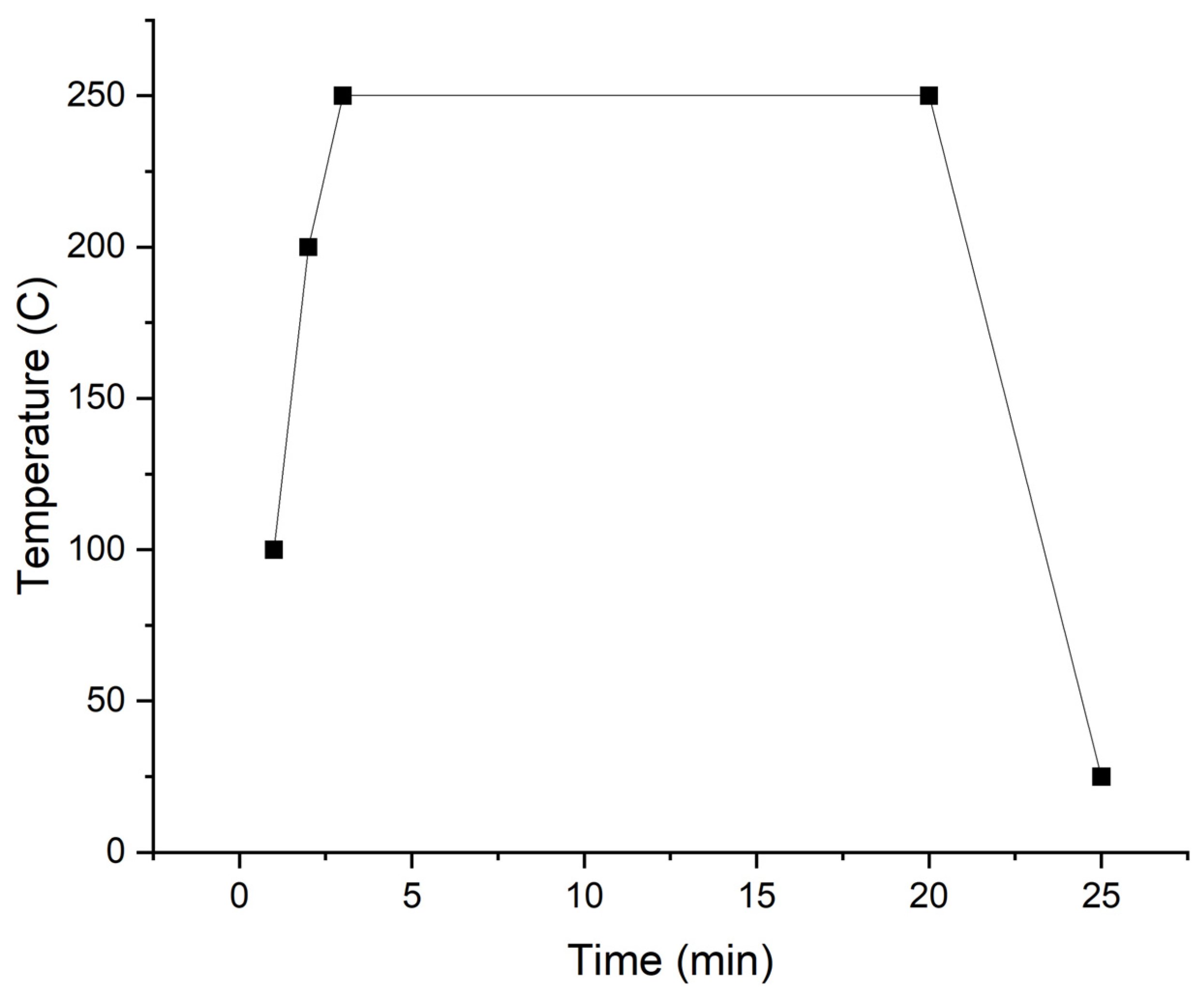
2.1. Material Preparation

Experimental samples were prepared using laser scribing of as-cut (100), n-type wafers into 3 × 3 cm size. The initial thickness and resistivity of the wafers were 180 µm and 1–3.5 Ω·cm, respectively.
An HNA solution (1HNO3 (75%):1CH5COOH (99.7%):0.2HF(45%)) was used for surface damage removal. Following damage removal, the samples were cleaned in an RCA 2 (0.1HCl (37%):0.2H2O2 (30%):H2O) solution at 70 °C. Next, the samples were immersed in a low-concentration HF solution for the removal of native oxide. The last part of the sample preparation was cleaning the samples in an RCA 1 (0.2NH4OH (30%):H2O2:H2O) solution at 70–75 °C (while forming so-called “RCA oxide”).

2.2. ALD Deposition

Atomic layer deposition of titanium oxide in this work was conducted from two different precursors TDMA-Ti and TiCl4. Two different ALD systems were used: Beneq TFS-500 for deposition of TiOx using a TiCl4 precursor (at Aalto University, Helsinki, Finland) and Savannah S100 with TDMA-Ti as a precursor (at the Norwegian University of Science and Technology, Trondheim, Norway). In both cases, the second precursor was water. Each deposition set consisted of six samples, which, after the deposition, were split into three parallels of two samples. Post-deposition annealing (PDA) was performed in a rapid thermal annealing system (RTP Allwin). The second part of this study consisted of stack layer deposition of aluminium oxide (AlOy) and TiOx. Deposition of the AlOy in the AlOy/TiOx stack was conducted using Trimethylaluminium (TMA) precursor as the first precursor and water as the second (on both ALD equipment Beneq TFS-500 and Savannah S100). The AlOy:TiOx deposition ratios were: 1:1, 1:5, 1:30, and 1:60, respectively. All experimental details are presented in Table 1.
Post-deposition annealing of the samples with the RTP system was conducted according to the RTP profile demonstrated in Figure 1 with the plateau temperatures outlined in Table 1.

2.3. Characterisation

After deposition and post-deposition annealing, the passivation and material properties of the thin films were studied. Minority carrier lifetime (MCLT) was measured using the transient photo-conductance decay (PCD) method with a Sinton WCT-120 tool, and the sheet resistance of the samples was determined using a CMT-SR2000N four-point probe. Five points per sample were measured using the four-point probe, and median values were calculated. Three samples per deposition condition such as thickness and deposition temperature were analysed. The samples with the highest MCLT and sheet resistance for both precursors were studied using TEM (transmission electron microscopy). Preliminary film thickness measurements were carried out using spectroscopic ellipsometry (Woollam M2000) for the TDMA-Ti precursor deposition. The thickness of the deposited TiOx films was also measured using TEM. The TEM analysis was performed with a Helios 5 plasma-focused ion beam (PFIB). Electron-deposited carbon and subsequently platinum were used as protection layers. Cross-section lift-out and thinning were performed using Xe ions, finishing with 2 kV ions. TEM/annular dark field scanning TEM (ADF-STEM) was performed using a double-corrected JEOL ARM-200F cold field emission microscope at 200 kV. Energy-dispersive X-ray spectroscopy (EDS) and electron energy loss spectroscopy (EELS) were performed using JEOL Centurio and GIF Quantum detectors. Scanning precession electron diffraction was performed with a JEOL 2100F microscope at 200 kV.

3. Results and Discussion
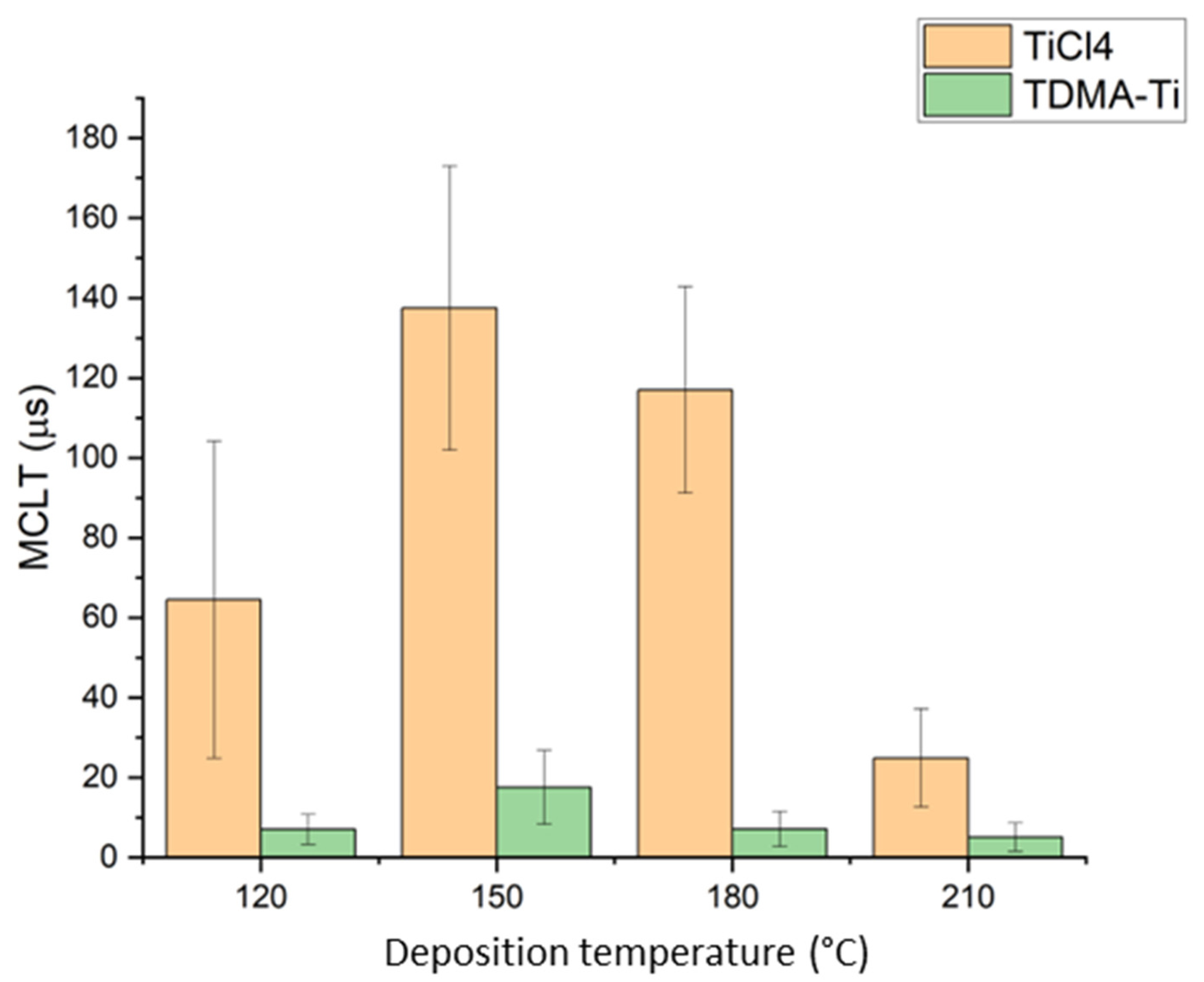
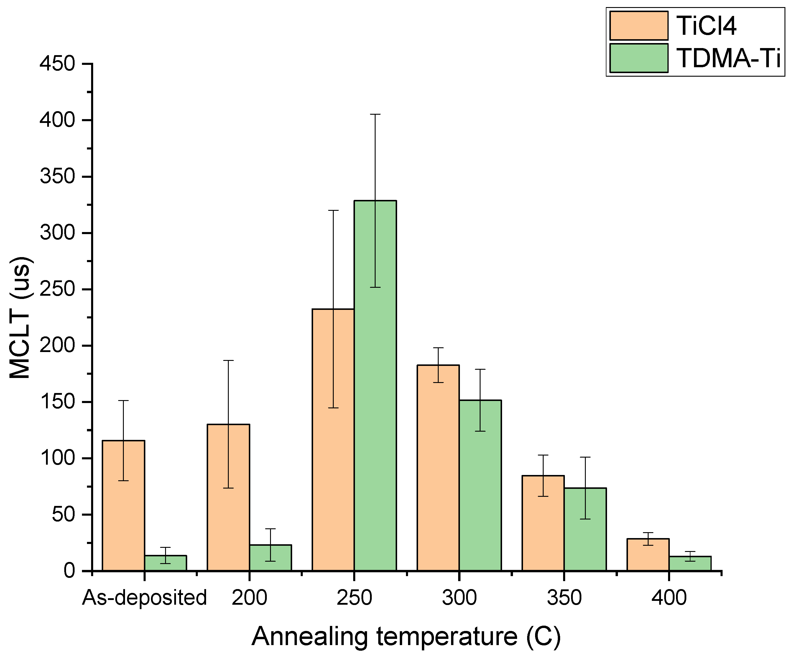
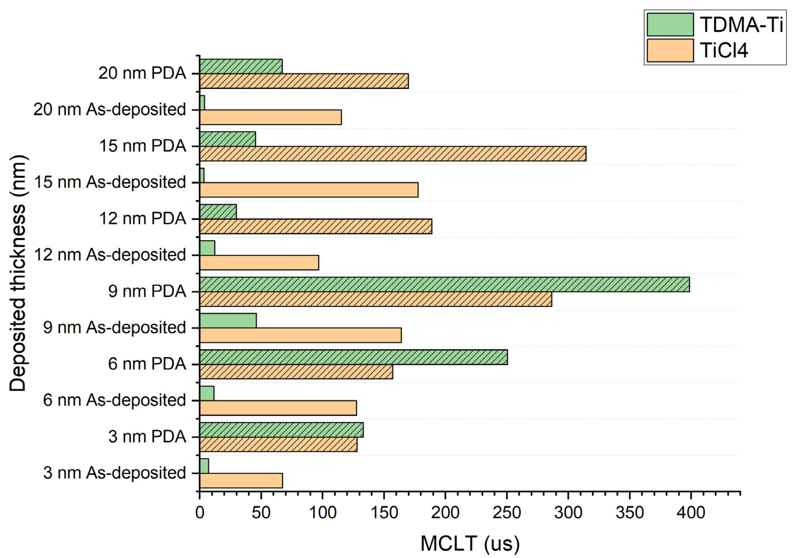
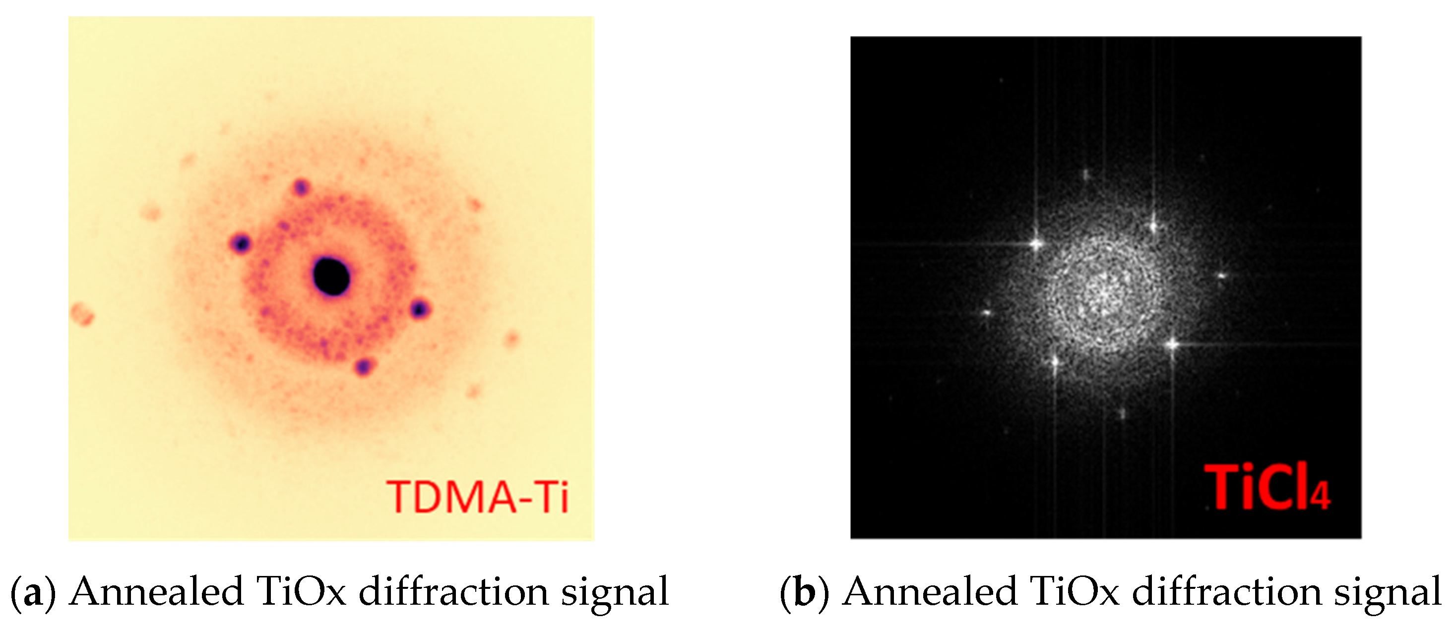
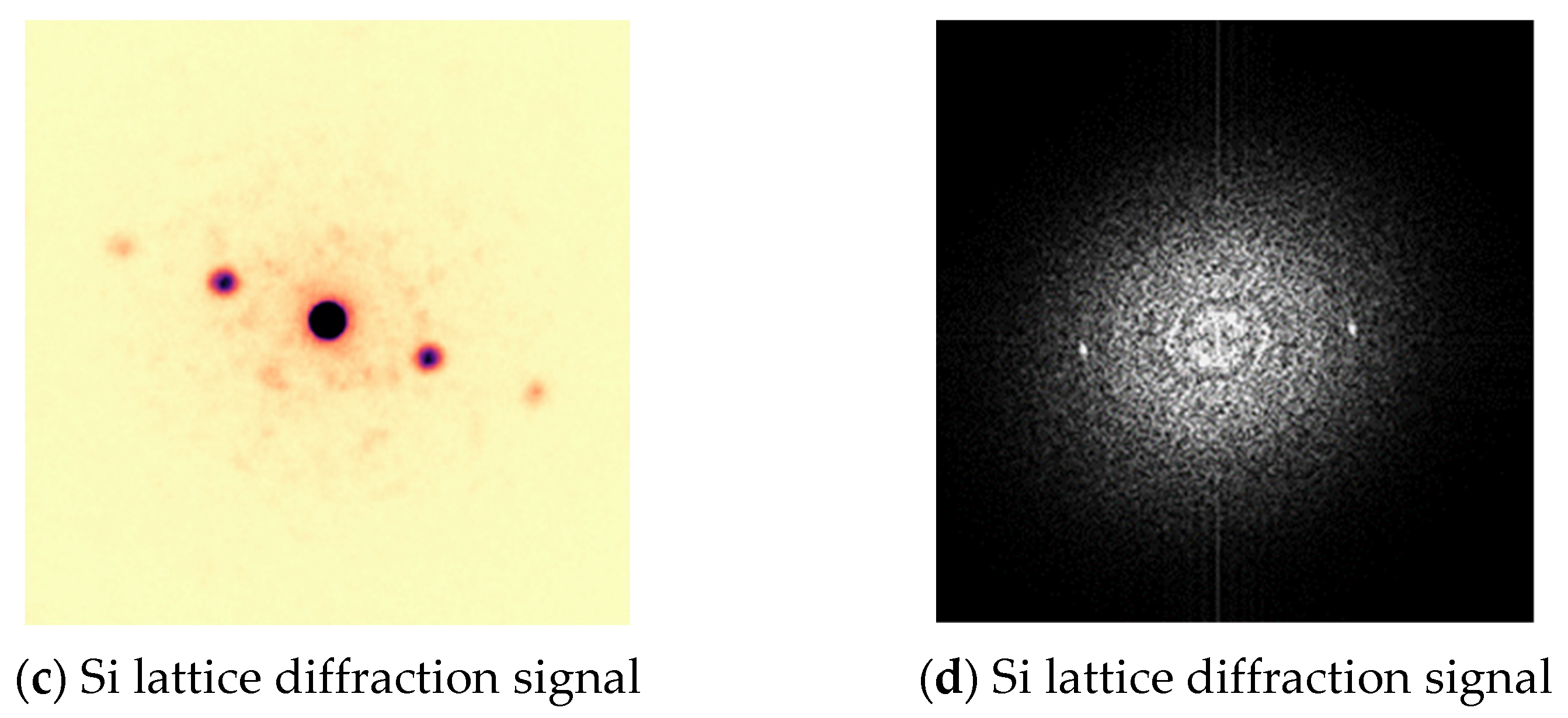
3.1. TiOx Films

The first part of this study concentrated on the deposition conditions for the two different TiOx precursors. For both precursors, titanium oxide was deposited in the temperature range from 120 °C to 200 °C. During the experiments, an intended 15 nm thick TiOx layer was deposited at these temperatures with subsequent µ-PCD measurements. Initial ellipsometry measurements showed a 1.5 nm average thickness error for the TDMA-Ti-deposited TiOx films for the temperature range 120–200 °C (see Supplementary Material for details). Thus, the growth per cycle rate (GPC) was assumed to be constant for the investigated temperature range, in accordance with the previously reported value of 0.5 Å/cycle [34]. Figure 2 presents the measured values of the minority carrier lifetime for the as-deposited samples obtained from the TiCl4 and TDMA-Ti precursors, respectively. As seen in Figure 2, the TiOx films deposited at 150 °C have the highest measured MCLT for both precursors and thus we conclude, in accordance with previous studies, that this temperature is most efficient in promoting the formation of the TiOx anatase phase [35].
The TiCl4 precursor films consistently display a higher minority carrier lifetime than the TDMA-Ti precursor. All MCLT results are, however, much lower than those presented in other studies [23,24]. This might be caused by the deposition recipe setup parameters or precursor distribution in the reactor. In some studies, the only reported results are obtained after post-deposition annealing, which has proven successful in increasing MCLT [24,26]. Thus, the samples deposited at 150 °C were annealed at 200 °C–400 °C for 20 min in N2 atmosphere with subsequent MCLT measurements. It was demonstrated that annealing at 250 °C significantly improves surface passivation for both precursors (Figure 3). The increase in MCLT for the annealed TiOx deposited from the TDMA-Ti is larger than that of TiCl4, making the effect of the precursor on the MCLT after annealing insignificant at temperatures above 200 °C. Such a difference in the post-annealing MCLT improvement might be related to initial differences in structure, density, or thickness of the as-deposited films which, following annealing, become less significant. A more detailed structural analysis of the as-deposited films may provide additional information on the morphological differences between the as-deposited films from TiCl4 and TDMA-Ti. Additionally, we can see that annealing at or above 300 °C does not positively affect MCLT. Finally, it is possible that at temperatures over 250 °C, crystal nucleation is initiated at multiple sites in the oxide film, which results in phase transformation of TiOx at these sites.
The thickness of the deposited layer is an important characteristic of the passivation- and carrier-selective layers. As such, TMOs (transparent metal oxides) typically display a clear correlation between the thickness of the deposited oxide and the passivation efficiency [36]. Thus, the relationship between thickness and passivation efficiency, as well as thickness and sheet resistance, were investigated for both precursors. TiOx was deposited with an intended thickness range of 3–20 nm at 150 °C, with subsequent annealing. MCLT and sheet resistance were measured both before and after annealing.
Figure 4 presents the measured MCLT as a function of the targeted TiOx thickness for TMDA-Ti and TiCl4 precursors for the samples deposited at 150 °C and annealed at 250 °C and for the non-annealed samples. In both cases, the passivation efficiency increased with TiOx layer thickness up to 9 nm. Above 9 nm thickness, the passivation efficiency decreased for the TDMA-Ti precursor. The annealing treatment did not provide a significant improvement for 12, 15, or 20 nm of deposited TiOx (TDMA-Ti). The reason for such poor response might be related to the thickness of the films. In the case of the reaction in the TiOx layer or the reaction between the TiOx layer and the Si/SiOy interface, for the thicker oxide layers, a longer annealing time may be required. Thus, further experiments correlating the post-deposition annealing time with layer thickness may be needed.
The sheet resistance of the TiOx layers deposited at 150 °C and annealed at 250 °C was measured using the four-probe method. Figure 5a presents the measured sheet resistance for films deposited with both precursors at different thicknesses of the titanium oxide. We can observe a clear trend in resistance increase with thickness for the TiCl4 precursor while the resistance of the layers deposited from TDMA-Ti remains in the range of 170–250 Ω/sq. For the 20 nm thickness TiOx deposited with the TiCl4 precursor, some measured resistance values are clear outliers (Figure 5b). Such abnormal values increase the median resistance and standard deviation. The low resistance of the TDMA-Ti (TiOx) might be due to a higher resistance-change threshold of the deposited TiOx caused by a change in the current path through the material. The TDMA-Ti-deposited TiOx film resistance may increase faster after a certain thickness higher than 20 nm, as in other Ti-based materials [37,38]. However, to prove this theory, additional experimental work is required.

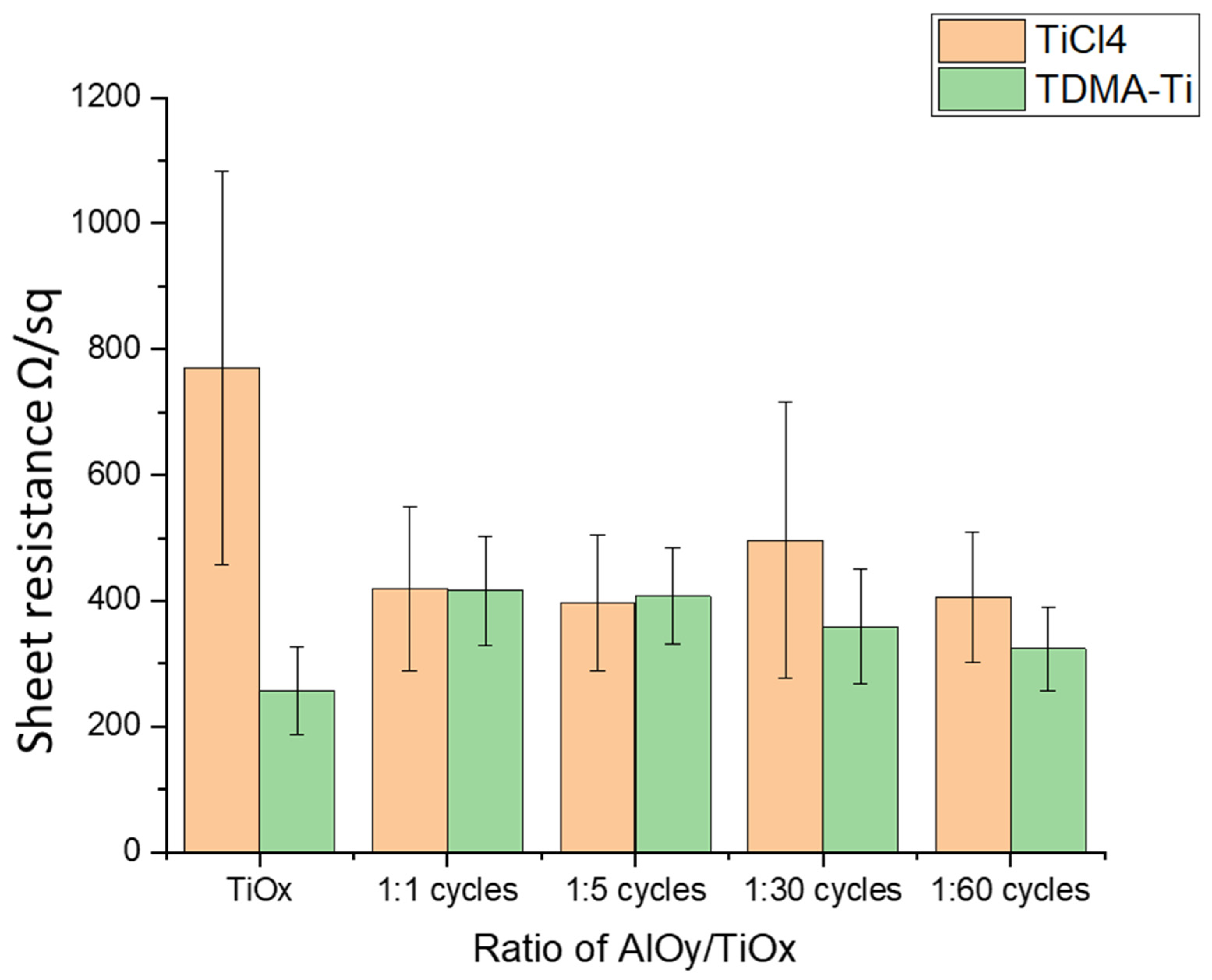
3.2. Al2O3/TiOx Stack Films

Techniques using aluminium oxide in a stack with titanium oxide [39] or aluminium-doped TiOx [24] are under development, mostly because of the improved conductivity of such layers in comparison to TiOx alone. Such passivation layers are one of the alternatives to ultra-thin a-Si:H passivation [40]. In this work, AlOy/TiOx stacks were studied as a possible alternative to mono-TiOx layers, quantifying the potential improvement for each precursor.
Figure 6 illustrates the effect of introducing aluminium oxide in the TiOx stack (intended 9 nm) for both precursors. For neither precursor, there is clear improvement in MCLT when introducing AlOy in the stack.
Following the MCLT analysis of the samples, the sheet resistance of the Al2O3/TiOx stacks was measured. In Figure 7, no clear differences in resistance between the precursor stacks were observed. However, resistance was reduced by more than 40% (770 Ω/sq to 405 Ω/sq) from the original values of the TiOx layer for the TICl4 precursor. The measured sheet resistance of the deposited AlOy/TiOx stacks was at approximately the same level for all AlOy/TiOx ratios. The measured sheet resistances are detailed in the Supplementary Materials.

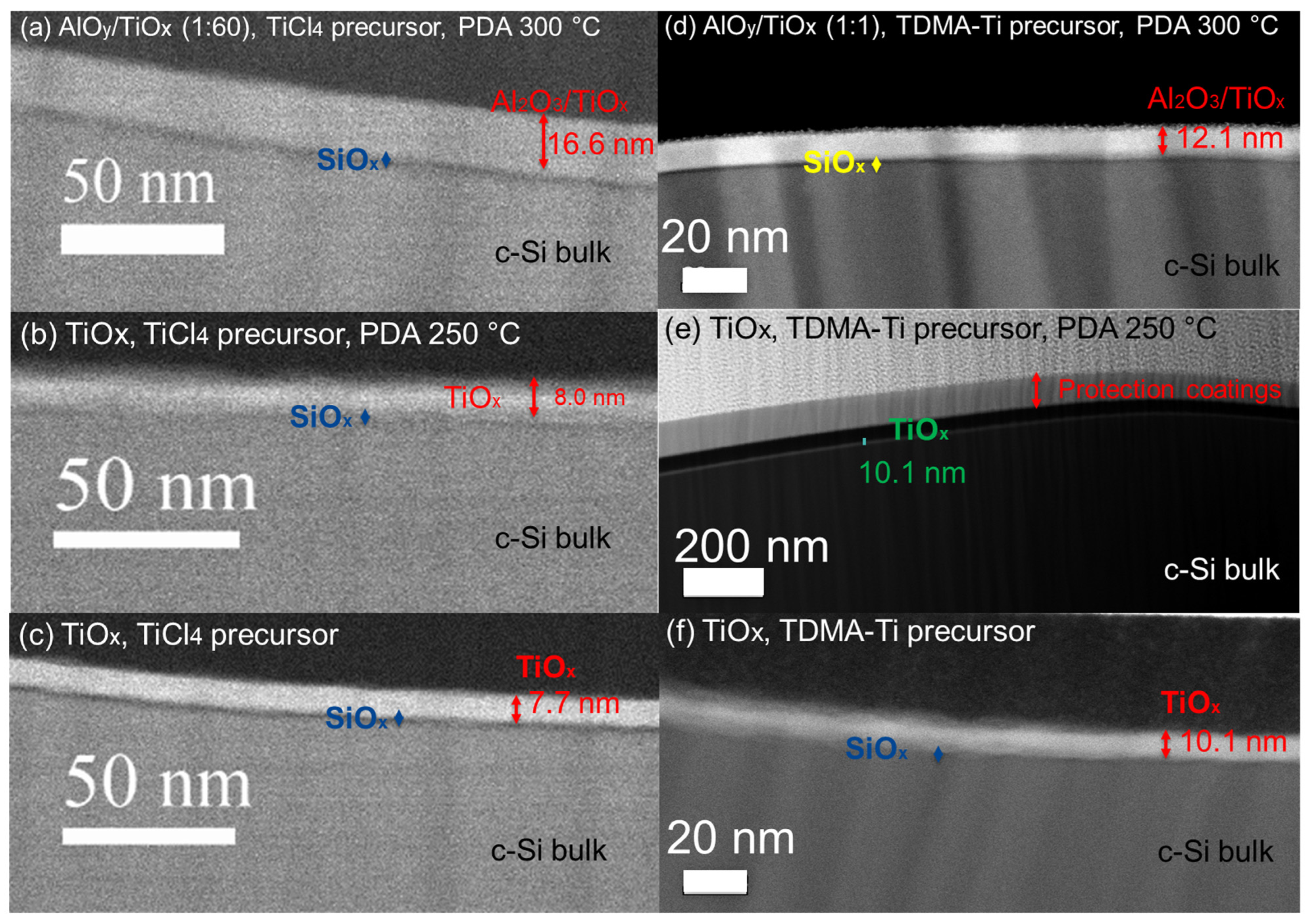
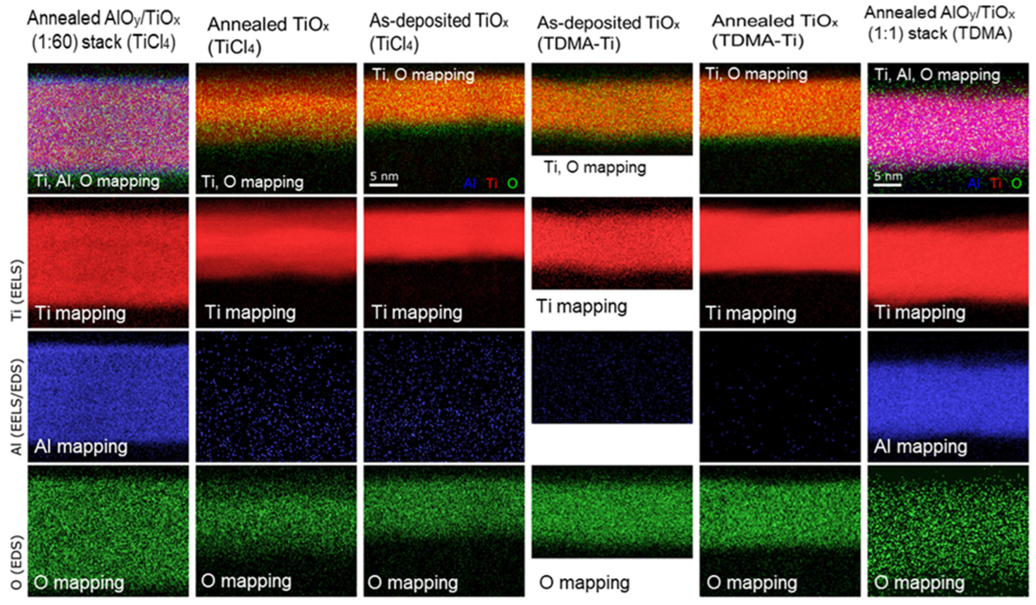
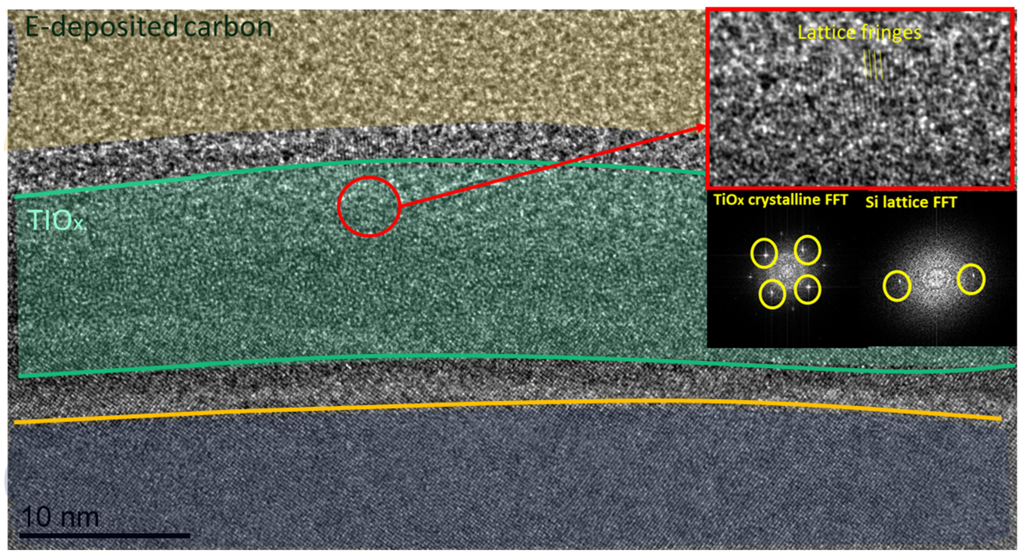
3.3. TEM Analysis of Deposited Films

In order to better understand the differences observed between precursors, a TEM analysis of three samples for each of the two titanium oxide ALD precursors was carried out. These included the targeted 9 nm of pure TiOx annealed and as-deposited, along with the targeted 9 nm deposited AlOy/TiOx stacks.
First the achieved, as opposed to targeted, TiOx and AlOy/TiOx layer thicknesses were measured. The actual deposited thickness of the targeted 9 nm layers for the TiCl4 precursor was 16.6 nm for the annealed AlOy/TiOx (1:60) stack (Figure 8a), while for the annealed TiOx (Figure 8b) and as-deposited TiOx (Figure 8c), the thicknesses were 8 nm and 7.7 nm, respectively. For the TDMA-Ti precursor, the thickness was 12.1 nm for the annealed AlOy/TiOx (1:1) stack (Figure 8d), 10.1 nm for the as-deposited TiOx (Figure 8f), and 10.1 nm for the annealed TiOx (Figure 8e). As such, the intended deposited thicknesses and the actual thickness of the layers were slightly different for the single TiOx deposited films. The thickness of the AlOy/TiOx (1:60) stack using the TiCl4 precursor was 7.6 nm thicker than expected, while the TDMA-Ti precursor thickness of the AlOy/TiOx (1:1) stack was 3.1 nm thicker than intended. However, the pure TiOx layers deposited using the TiCl4 precursors are somewhat thinner than intended, while those deposited using TDMA-Ti are slightly thicker than expected.
As the initial ellipsometry measurements showed small thickness deviations for the TDMA-Ti-deposited TiOx films, these measurements were not continued for the bulk of samples. Hence, there may be differences in the thicknesses measured using ellipsometry and those measured using TEM. Further work to compare the thicknesses obtained using TEM and ellipsometry should hence be performed in future studies.
The TEM-measured thicknesses of the AlOy/TiOx stacks also deviate from those intended. During the deposition, precursors were pulsed into the reactor one by one after a certain amount of time (purging time). It is possible that the purging time for AlOy was not long enough to remove the products of the TMA and H2O precursor reaction [41], which resulted in the additional growth of the AlOy layer during the next pulses of water precursor into the reactor. Thus, during the deposition of TiOx and AlOy, additional TMA precursors may remain in the reactor, resulting in the additional growth of the oxide layer.
Elemental mapping using a combination of electron energy loss spectroscopy (EELS) and energy-dispersive X-ray spectroscopy (EDS) was also carried out for each of the samples (Figure 9). While EDS is not a quantitatively reliable tool, it gives a good indication of the relative concentration of elements. A comparison of the AlOy/TiOx-deposited stacks revealed that Al is distributed across the whole oxide layer for both precursors, while the deposition process was performed layer-by-layer. In the case of the 1:1 AlOy/TiOx ratio, such an Al distribution might be possible due to the proposed TDMA-Ti precursor residue in the reactor. In the case of the 1:60 ratio, where only 1 deposition cycle of AlOy was performed for 60 deposition cycles of the TiOx, and each cycle had its own purging, the probability of the AlOy being distributed across the whole oxide layer caused by TDMA-Ti precursor residues is low. However, the thickness of the deposited layer per cycle is approximately 0.05 nm for TiOx, while it is 0.1 nm for the AlOy [34]. As a result, for the 1:1 cycle deposition, the thin film will consist of 0.05–0.1 nm thick layers, which are not possible to identify with the resolution of the TEM instrument used in this work. Thus, the conclusion is that the EDS analysis does not have a high enough resolution to give an accurate composition of the individual deposited layers.
For both the as-deposited and annealed TiOx layers, a difference in the Ti:O ratio between precursors was found. For both precursors, there was also a difference between the as-deposited and annealed TiOx, which corresponded with the layer thickness differences. The composition of the TiOx films from elemental mapping measured in atomic percentage using EDS analysis is presented in Table 2. Although the values obtained using EDS cannot be claimed to be quantitatively exact, relative differences are more reliable.
As summarised in Table 2 and suggested by the MCLT measurement results, it is possible that the oxygen to titanium content dictates passivation properties. We can see that the annealed samples of both precursors display a higher oxygen-to-titanium ratio and a higher minority carrier lifetime than the as-deposited samples. This phenomenon was also observed in previous work for the E-beam evaporated TiOx layer [42], indicating that a higher oxygen content improves the passivation properties of the TiOx layer.
The TEM work revealed that the TDMA-Ti-deposited TiOx was 2 nm thicker than the TiCl4-based film. Such a thickness difference might affect the MCLT, as passivation tends to increase with the thickness of the oxide layer [43,44]. The same trend is presented in this work for the annealed TiOx from 3 to 9 nm thickness (Figure 2). This theory would also explain the higher MCLT of the TDMA-Ti-deposited TiOx layer (at thicknesses ≤ 9 nm intended thickness) over the TiCl4 precursor. However, if we assume that each deposited TiOx TDMA-Ti thickness is 2 nm thicker than intended, in accordance with Figure 8, the 9 nm thick layer of TDMA-Ti TiOx still has a relatively higher MCLT than the 12 nm thick TiCl4-based TiOx film.
During the high-resolution TEM analysis of the annealed samples obtained from the TiCl4 precursor, crystallised areas were discovered. Figure 10 shows a high-resolution TEM image of annealed TiOx (TiCl4) film (8 nm) with faint signals of crystallinity. For neither of the AlOy/TiOx stacks (TiCl4) nor the as-deposited TiOx (TiCl4) samples, lattice diffraction was indicated. For the annealed TDMA-Ti precursor samples, the same signals of crystallinity were also revealed with electron diffraction of the selected area. Figure 11 shows the diffraction patterns in the annealed TiOx for both precursors. Like the TiCl4 precursor, the as-deposited samples from TDMA-Ti showed no traces of crystallinity.
Signs of nano-crystallinity for annealed TiOx have been reported in previous studies. Phase-change from amorphous TiOx to anatase in atomic-layer-deposited TiOx (from titanium IV isopropoxide TTIP precursor) was discovered in a post-deposition annealing process at 450 °C [45]. In our case, the temperature of the PDA process was lower at 250 °C, and the crystallinity signal was weak. However, this may indicate that already at 250 °C, the phase-change process is initiated in ultra-thin TiOx films. In order to gain valuable information on the crystallinity of TiOx films, conducting grazing incidence X-ray diffraction analysis must be considered in future research.
Crystallinity might affect passivation quality. During the TiOx phase change process, additional oxygen might be absorbed, which will decrease oxygen deficiency in the film. Another possible reason for the improvement in the measured MCLT after the PDA process is the additional growth of the silicon oxide (SiO2) at the Si/TiOx interface [42,46]. Previous studies have presented opposite effects on passivation quality with the crystallisation of TiOx [46]. However, a previous study by the current first author on E-beam-deposited TiOx indicated the same passivation improvement with film crystallisation [42].
Neither of the annealed AlOy/TiOx films deposited from TiCl4 and TDMA-Ti precursors showed signs of crystallinity despite a higher annealing temperature (300 °C). These samples also showed less improvement in passivation quality after the PDA process. This might be related to a too-low temperature for “activation” of AlOy passivation [47] in conjunction with the absence of a real stack, as aluminium is distributed across the whole film. This probably affected the sheet resistance of the mixed oxide layer in comparison with TiOx alone, as Al is widely used as a dopant to improve the conductivity of MO films [24,48]. The aluminium oxide presence might also hinder the crystal formation (phase change) of TiOx. The reason for such an effect might be the formation of a new aluminium/titanium compound (Alx-Oy-Tiz) in the passivation layer, resulting in the distribution of Al across the oxide layer. Thus, a different temperature is required to improve the passivation quality of the layer as well as initiate a phase change process for TiOx.

4. Conclusions

This work aimed at comparing titanium oxide precursors (TiCl4 and TDMA-Ti) for atomic layer deposition of passivating TiOx. The precursors were compared with respect to the deposition temperature, post-deposition annealing composition, and properties of deposited films.
A deposition temperature of 150 °C was found to be optimal for both precursors. It was confirmed that post-deposition annealing of the deposited TiOx improves the passivation quality of the oxides. The optimal post-deposition annealing temperature of 250 °C was also similar for the two precursors.
The maximum achieved minority carrier lifetime (τeff) for the deposited 9 nm of TiOx was 398 µs for the TDMA-Ti precursor and 286 µs for TiCl4. A TEM analysis of the as-deposited and annealed TiOx revealed signals of nano-crystallinity for the post-deposition annealed TiOx films for both precursors, indicating that a phase change of the atomic-layer-deposited TiOx possibly starts at 250 °C. However, there is no evidence of a correlation between crystallinity and passivation improvement.
Aluminium oxide (AlOy)/titanium oxide (TiOx) stacks showed higher passivation quality than single TiOx films for both precursors with a maximum (τeff) of 311 µs for the TiCl4 precursor. For the TiCl4 precursor, the passivation quality increased with a decreasing AlOy:TiOx cycle ratio (from 1:1 to 1:60), while for the TDMA-Ti precursor, it was vice versa (from 1:60 to 1:1). Furthermore, sheet resistance measurements showed that the AlOy/TiOx stack had much lower resistance than the pure TiOx layer. Thus, we conclude that the Al presence in TiOx films decreases sheet resistance, while additional experimental work, such as optimising annealing temperature, is required to improve the passivation quality of the AlOy/TiOx stack.

5. Future Perspectives

In order to continue the work of the current study, some future perspectives may be presented: The performance of the deposition process for the two different ALD equipment units should be tuned to the same GPC for the two precursors and, if possible, also ensure the same precursor distribution during the deposition. This might be helpful to better evaluate the correlation between deposited thickness and differences in sample characteristics (e.g., MCLT). Moreover, further post-deposition analysis of the obtained films such as grazing incidence X-ray diffraction analysis and transfer length measurements (TLM) will give a better understanding of film conductivity and crystallinity. Further experimental work investigating the effect of post-annealing duration on different TiOx film thicknesses is recommended.

Supplementary Materials

The following supporting information can be downloaded at: https://www.mdpi.com/article/10.3390/ma16165522/s1.

Author Contributions

Methodology, V.M., O.L., H.L., V.V., M.D.S. and G.T.; Formal analysis, V.M.; Investigation, V.M., O.L. and S.W.; Resources, H.S.; Writing—original draft, V.M.; Writing—review & editing, V.M. and G.T.; Supervision, H.S., M.D.S. and G.T. All authors have read and agreed to the published version of the manuscript.

Funding

The FIB preparation was performed at the SMART-H infrastructure, funded by The Research Council of Norway (RCN), grant 296197. The TEM work was carried out at the NORTEM infrastructure, RCN grant 197405.

Institutional Review Board Statement

Not applicable.

Informed Consent Statement

Not applicable.

Data Availability Statement

Available on request to authors.

Acknowledgments

The authors gratefully acknowledge financial support from the Research Council of Norway through the research project “DiamApp” (project no. 280831). The authors acknowledge the provision of facilities and technical support by Micronova Nanofabrication Centre in Espoo, Finland within the OtaNano research infrastructure at Aalto University.

Conflicts of Interest

The authors declare no conflict of interest.

References

  1. Han, X.; Ouyang, M.; Lu, L.; Li, J. Cycle Life of Commercial Lithium-Ion Batteries with Lithium Titanium Oxide Anodes in Electric Vehicles. Energies 2014, 7, 4895–4909. [Google Scholar] [CrossRef] [Green Version]
  2. Jackson, M.J.; Kopac, J.; Balazic, M.; Bombac, D.; Brojan, M.; Kosel, F. Titanium and Titanium Alloy Applications in Medicine. In Surgical Tools and Medical Devices; Ahmed, W., Jackson, M.J., Eds.; Springer International Publishing: Cham, Switzerland, 2016; pp. 475–517. [Google Scholar] [CrossRef]
  3. Li, W.; Fu, T.; Xie, F.; Yu, S.; He, S. The multi-staged formation process of titanium oxide nanotubes and its thermal stability. Mater. Lett. 2007, 61, 730–735. [Google Scholar] [CrossRef]
  4. Cui, J.; Allen, T.; Wan, Y.; Mckeon, J.; Samundsett, C.; Yan, D.; Zhang, X.; Cui, Y.; Chen, Y.; Verlinden, P.; et al. Titanium oxide: A re-emerging optical and passivating material for silicon solar cells. Sol. Energy Mater. Sol. Cells 2016, 158, 115–121. [Google Scholar] [CrossRef]
  5. Afzal, A.; Habib, A.; Ulhasan, I.; Shahid, M.; Rehman, A. Antireflective Self-Cleaning TiO2 Coatings for Solar Energy Harvesting Applications. Front. Mater. 2021, 8, 687059. [Google Scholar] [CrossRef]
  6. Melskens, J.; van de Loo, B.W.H.; Macco, B.; Black, L.E.; Smit, S.; Kessels, W.M.M. Passivating Contacts for Crystalline Silicon Solar Cells: From Concepts and Materials to Prospects. IEEE J. Photovoltaics 2018, 8, 373–388. [Google Scholar] [CrossRef] [Green Version]
  7. Richards, B.S. Novel Uses of Titanium Dioxide for Silicon Solar Cells; UNSW Sydney: Kensington, Australia, 2002. [Google Scholar]
  8. Horprathum, M.; Chindaudom, P.; Limsuwan, P. A Spectroscopic Ellipsometry Study of TiO2 Thin Films Prepared by dc Reactive Magnetron Sputtering: Annealing Temperature Effect. Chin. Phys. Lett. 2007, 24, 1505–1508. [Google Scholar] [CrossRef]
  9. Eiamchai, P.; Chindaudom, P.; Pokaipisit, A.; Limsuwan, P. A spectroscopic ellipsometry study of TiO2 thin films prepared by ion-assisted electron-beam evaporation. Curr. Appl. Phys. 2009, 9, 707–712. [Google Scholar] [CrossRef]
  10. Hitosugi, T.; Yamada, N.; Nakao, S.; Hirose, Y.; Hasegawa, T. Properties of TiO2-based transparent conducting oxides. Phys. Status Solidi (a) 2010, 207, 1529–1537. [Google Scholar] [CrossRef]
  11. Mazumder, M.K.; Sharma, R.; Biris, A.S.; Zhang, J.; Calle, C.; Zahn, M. Self-Cleaning Transparent Dust Shields for Protecting Solar Panels and Other Devices. Part. Sci. Technol. 2007, 25, 5–20. [Google Scholar] [CrossRef]
  12. Kang, X.; Liu, S.; Dai, Z.; He, Y.; Song, X.; Tan, Z. Titanium Dioxide: From Engineering to Applications. Catalysts 2019, 9, 191. [Google Scholar] [CrossRef] [Green Version]
  13. Nowotny, J. Oxide Semiconductors for Solar Energy Conversion: Titanium Dioxide; CRC Press: Boca Raton, FL, USA, 2011. [Google Scholar]
  14. Zeng, Y.; Tong, H.; Quan, C.; Cai, L.; Yang, Z.; Chen, K.; Yuan, Z.; Wu, C.-H.; Yan, B.; Gao, P.; et al. Theoretical exploration towards high-efficiency tunnel oxide passivated carrier-selective contacts (TOPCon) solar cells. Sol. Energy 2017, 155, 654–660. [Google Scholar] [CrossRef]
  15. Kamisaka, H.; Adachi, T.; Yamashita, K. Theoretical study of the structure and optical properties of carbon-doped rutile and anatase titanium oxides. J. Chem. Phys. 2005, 123, 084704. [Google Scholar] [CrossRef] [PubMed]
  16. Murakami, N.; Kamai, T.-A.; Tsubota, T.; Ohno, T. Novel hydrothermal preparation of pure brookite-type titanium(IV) oxide nanocrystal under strong acidic conditions. Catal. Commun. 2009, 10, 963–966. [Google Scholar] [CrossRef] [Green Version]
  17. Bakri, A.S.; Sahdan, M.Z.; Adriyanto, F.; Raship, N.A.; Said, N.D.M.; Abdullah, S.A.; Rahim, M.S. Effect of annealing temperature of titanium dioxide thin films on structural and electrical properties. AIP Conf. Proc. 2017, 1788, 030030. [Google Scholar] [CrossRef] [Green Version]
  18. Kukli, K.; Ritala, M.; Schuisky, M.; Leskelä, M.; Sajavaara, T.; Keinonen, J.; Uustare, T.; Hårsta, A. Atomic layer deposition of titanium oxide from TiI4 and H2O2. Chem. Vap. Depos. 2000, 6, 303–310. [Google Scholar] [CrossRef]
  19. Jang, H.K.; Whangbo, S.W.; Choi, Y.K.; Chung, Y.D.; Jeong, K.; Whang, C.N.; Lee, Y.S.; Lee, H.-S.; Choi, J.Y.; Kim, G.H.; et al. Titanium oxide films on Si(100) deposited by e-beam evaporation. J. Vac. Sci. Technol. A 2000, 18, 2932–2936. [Google Scholar] [CrossRef]
  20. César, R.; Barros, A.; Doi, I.; Diniz, J.; Swart, J. Thin titanium oxide films obtained by RTP and by sputtering. In Proceedings of the 2014 29th Symposium on Microelectronics Technology and Devices (SBMicro), Aracaju, Brazil, 1–5 September 2014; pp. 1–4. [Google Scholar]
  21. Mathur, S.; Kuhn, P. CVD of titanium oxide coatings: Comparative evaluation of thermal and plasma assisted processes. Surf. Coatings Technol. 2006, 201, 807–814. [Google Scholar] [CrossRef]
  22. Meng, L.-J.; dos Santos, M. Investigations of titanium oxide films deposited by d.c. reactive magnetron sputtering in different sputtering pressures. Thin Solid Films 1993, 226, 22–29. [Google Scholar] [CrossRef]
  23. Liao, B.; Hoex, B.; Aberle, A.G.; Chi, D.; Bhatia, C.S. Excellent c-Si surface passivation by low-temperature atomic layer deposited titanium oxide. Appl. Phys. Lett. 2014, 104, 253903. [Google Scholar] [CrossRef]
  24. Liu, Y.; Sang, B.; Hossain, A.; Gao, K.; Cheng, H.; Song, X.; Zhong, S.; Shi, L.; Shen, W.; Hoex, B.; et al. A novel passivating electron contact for high-performance silicon solar cells by ALD Al-doped TiO2. Sol. Energy 2021, 228, 531–539. [Google Scholar] [CrossRef]
  25. Yu, I.-S.; Chang, I.-H.; Cheng, H.-E.; Lin, Y.-S. Surface passivation of c-Si by atomic layer deposition TiO2 thin films deposited at low temperature. In Proceedings of the 2014 IEEE 40th Photovoltaic Specialist Conference (PVSC), Denver, CO, USA, 8–13 June 2014; pp. 1271–1274. [Google Scholar] [CrossRef]
  26. Yu, I.-S.; Wang, Y.-W.; Cheng, H.-E.; Yang, Z.-P.; Lin, C.-T. Surface Passivation and Antireflection Behavior of ALD on n-Type Silicon for Solar Cells. Int. J. Photoenergy 2013, 2013, 431614. [Google Scholar] [CrossRef] [Green Version]
  27. Hsu, C.-H.; Chen, K.-T.; Huang, P.-H.; Wu, W.-Y.; Zhang, X.-Y.; Wang, C.; Liang, L.-S.; Gao, P.; Qiu, Y.; Lien, S.-Y.; et al. Effect of Annealing Temperature on Spatial Atomic Layer Deposited Titanium Oxide and Its Application in Perovskite Solar Cells. Nanomaterials 2020, 10, 1322. [Google Scholar] [CrossRef]
  28. Peng, T.; Xiao, X.; Ren, F.; Xu, J.; Zhou, X.; Mei, F.; Jiang, C. Influence of annealing temperature on the properties of TiO2 films annealed by ex situ and in situ TEM. J. Wuhan Univ. Technol. Sci. Ed. 2012, 27, 1014–1019. [Google Scholar] [CrossRef]
  29. Parsons, G.N.; George, S.M.; Knez, M. Progress and future directions for atomic layer deposition and ALD-based chemistry. MRS Bull. 2011, 36, 865–871. [Google Scholar] [CrossRef] [Green Version]
  30. Xie, Q.; Jiang, Y.-L.; Detavernier, C.; Deduytsche, D.; Van Meirhaeghe, R.L.; Ru, G.-P.; Li, B.-Z.; Qu, X.-P. Atomic layer deposition of TiO2 from tetrakis-dimethyl-amido titanium or Ti isopropoxide precursors and H2O. J. Appl. Phys. 2007, 102, 083521. [Google Scholar] [CrossRef]
  31. Park, H.K.; Yang, B.S.; Park, S.; Kim, M.S.; Shin, J.C.; Heo, J. Purge-time-dependent growth of ZnO thin films by atomic layer deposition. J. Alloys Compd. 2014, 605, 124–130. [Google Scholar] [CrossRef]
  32. Saarenpää, H.; Niemi, T.; Tukiainen, A.; Lemmetyinen, H.; Tkachenko, N. Aluminum doped zinc oxide films grown by atomic layer deposition for organic photovoltaic devices. Sol. Energy Mater. Sol. Cells 2010, 94, 1379–1383. [Google Scholar] [CrossRef]
  33. Merisalu, J.; Arroval, T.; Kasikov, A.; Kozlova, J.; Rähn, M.; Ritslaid, P.; Aarik, J.; Tamm, A.; Kukli, K. Engineering of atomic layer deposition process for titanium-aluminum-oxide based resistively switching medium. Mater. Sci. Eng. B 2022, 282. [Google Scholar] [CrossRef]
  34. Peron, M.; Cogo, S.; Bjelland, M.; Bin Afif, A.; Dadlani, A.; Greggio, E.; Berto, F.; Torgersen, J. On the evaluation of ALD TiO2, ZrO2 and HfO2 coatings on corrosion and cytotoxicity performances. J. Magnes. Alloy. 2021, 9, 1806–1819. [Google Scholar] [CrossRef]
  35. Hanaor, D.A.H.; Sorrell, C.C. Review of the anatase to rutile phase transformation. J. Mater. Sci. 2010, 46, 855–874. [Google Scholar] [CrossRef] [Green Version]
  36. Macco, B.; Deligiannis, D.; Smit, S.; van Swaaij, R.A.C.M.M.; Zeman, M.; Kessels, W.M.M. Influence of transparent conductive oxides on passivation of a-Si:H/c-Si heterojunctions as studied by atomic layer deposited Al-doped ZnO. Semicond. Sci. Technol. 2014, 29, 122001. [Google Scholar] [CrossRef]
  37. Musschoot, J.; Xie, Q.; Deduytsche, D.; Berghe, S.V.D.; Van Meirhaeghe, R.; Detavernier, C. Atomic layer deposition of titanium nitride from TDMAT precursor. Microelectron. Eng. 2009, 86, 72–77. [Google Scholar] [CrossRef]
  38. Fox, G.R.; Potrepka, D.M.; Polcawich, R.G. Dependence of {111}-textured Pt electrode properties on TiO2 seed layers formed by thermal oxidation. J. Mater.Sci. Mater. Electron. 2018, 29, 412–426. [Google Scholar] [CrossRef]
  39. Temperton, R.H.; Gibson, A.; O’Shea, J.N. In situ XPS analysis of the atomic layer deposition of aluminium oxide on titanium dioxide. Phys. Chem. Chem. Phys. 2018, 21, 1393–1398. [Google Scholar] [CrossRef]
  40. Cheng, X.; Marstein, E.S.; Haug, H.; Di Sabatino, M. Double Layers of Ultrathin a-Si:H and SiNx for Surface Passivation of n-type Crystalline Si Wafers. Energy Procedia 2016, 92, 347–352. [Google Scholar] [CrossRef] [Green Version]
  41. Weckman, T.; Laasonen, K. First principles study of the atomic layer deposition of alumina by TMA–H 2 O-process. Phys. Chem. Chem. Phys. 2015, 17, 17322–17334. [Google Scholar] [CrossRef] [Green Version]
  42. Matkivskyi, V.; Lee, Y.; Seo, H.S.; Lee, D.-K.; Park, J.-K.; Kim, I. Electronic-beam evaporation processed titanium oxide as an electron selective contact for silicon solar cells. Curr. Appl. Phys. 2021, 32, 98–105. [Google Scholar] [CrossRef]
  43. Rafique, R.; Tonny, K.N.; Sharmin, A.; Mahmood, Z.H. Study on the Effect of Varying Film Thickness on the Transparent Conductive Nature of Aluminum Doped Zinc Oxide Deposited by Dip Coating. Mater. Focus 2018, 7, 707–713. [Google Scholar] [CrossRef]
  44. Kale, A.S.; Nemeth, W.; Harvey, S.P.; Page, M.; Young, D.L.; Agarwal, S.; Stradins, P. Effect of silicon oxide thickness on polysilicon based passivated contacts for high-efficiency crystalline silicon solar cells. Sol. Energy Mater. Sol. Cells 2018, 185, 270–276. [Google Scholar] [CrossRef]
  45. Hussin, R.; Choy, K.L.; Hou, X.H. Growth of TiO2 Thin Films by Atomic Layer Deposition (ALD). Adv. Mater. Res. 2016, 1133, 352–356. [Google Scholar] [CrossRef]
  46. Chen, X.Y.; Lu, Y.F.; Tang, L.J.; Wu, Y.H.; Cho, B.J.; Xu, X.J.; Dong, J.R.; Song, W.D. Annealing and oxidation of silicon oxide films prepared by plasma-enhanced chemical vapor deposition. J. Appl. Phys. 2005, 97, 014913. [Google Scholar] [CrossRef]
  47. Dingemans, G.; Kessels, W. Status and prospects of Al2O3-based surface passivation schemes for silicon solar cells. J. Vac. Sci. Technol. A Vac.Surf. Film. 2012, 30, 040802. [Google Scholar] [CrossRef] [Green Version]
  48. Kelly, P.; Zhou, Y.; Postill, A. A novel technique for the deposition of aluminium-doped zinc oxide films. Thin Solid Films 2003, 426, 111–116. [Google Scholar] [CrossRef]
Figure 1. RTP system post-deposition annealing profile with a plateau of 250 °C.
Materials 16 05522 g001
Figure 2. As-deposited median values of measured MCLT for an intended 15 nm thick TiOx film deposited at different temperatures. Error bars illustrate the standard deviation for each condition/precursor.
Materials 16 05522 g002
Figure 3. Measured median MCLT of the deposited 9 nm TiOx films deposited at 150 °C, post-annealed at different temperatures. Error bars illustrate the standard deviation for each condition/precursor.
Materials 16 05522 g003
Figure 4. Measured median MCLT for the different deposited thicknesses of TiOx before and after PDA.
Materials 16 05522 g004
Figure 5. (a) Median sheet resistance measurement of the different thicknesses for the deposited TiOx films after PDA. (b) Resistance measurement data distribution for the TiCl4 precursor. Error bars illustrate the standard deviations for each condition/precursor.
Materials 16 05522 g005
Figure 6. Measured median MCLT of the deposited AlOy/TiOx stack depending on the AlOy:TiOx deposition cycle ratio after annealing at 300 °C. Error bars illustrate the standard deviations for each condition/precursor.
Materials 16 05522 g006
Figure 7. Measured median sheet resistance of the deposited AlOy/TiOx stack depending on the AlOy:TiOx deposition cycle ratio after annealing at 300 °C. Error bars illustrate the standard deviation for each condition/precursor.
Materials 16 05522 g007
Figure 8. ADF-STEM image showing the TiOx and AlOy/TiOx stack layers: (a) Annealed at 300 °C AlOy/TiOx stack (1:60), TiCl4 precursor, (b) annealed at 250 °C TiOx layer, TiCl4 precursor, (c) TiOx as-deposited, TiCl4 precursor, (d) annealed at 300 °C AlOy/TiOx stack (1:1), TDMA-Ti precursor, (e) annealed at 250 °C TiOx layer, TDMA-Ti precursor, and (f) TiOx as-deposited, TDMA-Ti precursor.
Materials 16 05522 g008
Figure 9. EDS/EELS elemental mapping of the samples analysed with TEM.
Materials 16 05522 g009
Figure 10. High-resolution TEM image showing the annealed TiOx sample (TiCl4 precursor) with Fourier transforms (FFTs) of the layer attached (FFT zone axis (001)).
Materials 16 05522 g010
Figure 11. Diffraction peaks from the selected area electron diffraction scanning for TiOx deposited with different precursors.
Materials 16 05522 g011aMaterials 16 05522 g011b
Table 1. Main experimental conditions.
Deposited Thickness of TiOx (nm)3, 6, 9,12, 15, 20
Deposition temperature of TiOx from TDMA-Ti (°C)120, 140, 150, 180, 200, 210
Post deposition annealing temperature (°C)200, 250, 300, 350, 400
Deposition temperature of TiOx from TiCl4 precursor (°C)120, 150, 180, 210
Deposition layer stack ration AlOy:TIOx1:1, 1:5, 1:30, 1:60
Table 2. Atomic percentage of the TEM EDS-analysed samples. Atomic percentage error indicates summed EDS fitting error during a measurement.
Ti, Atomic %O, Atomic %
As-deposited TiOx (TiCl4)22.83 ± 0.2577.17 ± 0.78
As-deposited TiOx (TDMA-Ti)29.53 ± 0.2170.47 ± 0.47
Annealed TiOx (TiCl4)20.76 ± 0.3179.24 ± 0.99
Annealed TiOx (TDMA-Ti)26.09 ± 0.2073.80 ± 0.48
Disclaimer/Publisher’s Note: The statements, opinions and data contained in all publications are solely those of the individual author(s) and contributor(s) and not of MDPI and/or the editor(s). MDPI and/or the editor(s) disclaim responsibility for any injury to people or property resulting from any ideas, methods, instructions or products referred to in the content.

