Article

Transmission Electron Microscopy Peeled Surface Defect of Perovskite Quantum Dots to Improve Crystal Structure

1
School of Chemical Engineering and Technology, Tianjin University, Tianjin 300350, China
2
State Key Laboratory of Reliability and Intelligence of Electrical Equipment, School of Materials Science and Engineering, Hebei University of Technology, Tianjin 300130, China
*
Author to whom correspondence should be addressed.
These authors contributed equally to this work.
Materials 2023, 16(17), 6010; https://doi.org/10.3390/ma16176010
Submission received: 9 June 2023 / Revised: 23 August 2023 / Accepted: 30 August 2023 / Published: 1 September 2023

Abstract

:
Transmission electron microscopy (TEM) is an excellent characterization method to analyze the size, morphology, crystalline state, and microstructure of perovskite quantum dots (PeQDs). Nevertheless, the electron beam of TEM as an illumination source provides high energy, which causes morphological variation (fusion and melting) and recession of the crystalline structure in low radiolysis tolerance specimens. Hence, a novel and facile strategy is proposed: electron beam peel [PbBr6]4− octahedron defects from the surface of QDs to optimize the crystal structure. TEM and high-angle annular dark-field scanning TEM (HAADF) tests indicate that the [PbBr6]4− octahedron would be peeled from the surface of QDs when QDs samples were irradiated under high-power irradiation, and then a clear image would be obtained. To avoid interference from a protective film of “carbon deposits” on the surface of the sample when using high resolution TEM, amorphous carbon film (15–20 nm) was deposited on the surface of QDs film and then characterized by TEM and HAADF. The detection consequences showed that the defection of PbBr2 on the surface of QDs will gradually disappear with the extension of radiation time, which further verifies the conjecture.

1. Introduction

Metal halide perovskite quantum dots (PeQDs) have come into public view as superior semiconductor luminescent materials owing to their adjustable band gap, excellent electroluminescence, high charge mobility, long carrier lifetime, and high photoluminescence quantum yield [1,2,3,4,5,6]. In addition, because of their excellent properties, perovskites have shown great prospects in optoelectronic fields and have been successfully used in photovoltaic cells, photodetectors, lasers, light-emitting diodes, and many other fields [7,8,9,10,11]. In order to achieve both intuitive and convenient detection of QDs, especially in terms of their size, morphology, crystalline state, and microstructure, an excellent characterization method is urgently needed. Transmission electron microscopy (TEM) with high resolution and magnification is one of the most crucial tools for crystal structure and property characterizations of QDs [12,13]. However, the electron beam of TEM as an illumination source provides high energy, which causes morphological variation (fusion and melting) and recession of the crystalline structure in low radiolysis tolerance specimens [14,15,16]. PeQDs, a typical electron beam-sensitive material exposed to hundreds to thousands of electrons, would break down after being focused onto the microscopy and then arise radiation defects [17]. At present, the effect of low-energy electrons on the crystal surface properties has been reported, but the influence of electron beams on the crystal structure of PeQDs has not been studied [18,19]. As a result, the quality and reliability of reported imaging results are frequently questioned. It’s practical significance to achieve lower-damaged characterization of morphology, particle size, and crystalline state of PeQDs.
In response to the phenomenon of electron beam irradiation degradation of CsPbX3, researchers use different methods to increase imaging resolution, such as low-voltage high-resolution electron microscopy (LVHREM), cryo-TEM, carbon sedimentation, and so on [20,21,22,23]. For example, by reducing the irradiation dose rate combined with outgoing wave reconstruction, Yu revealed the microstructure of CsPbBr3 using spherical aberration-corrected high-resolution transmission electron microscopy (AC-HRTEM) with an accelerating voltage of 80 kV [24]. Dos Reis confirmed the tetragonal phase structure of CsPbBr3 PeQDs in terms of their diffraction pattern and higher-order Laue zone symmetry using converging beam electron diffraction (CBED). Furthermore, Dos Reis obtained an image of Br under low dose conditions combined with electron stack diffraction imaging, which provided a new solution for imaging PeQDs materials [25]. Li acquired diffraction images of the atomic structure of MAPbI3 utilizing cryo-TEM and quantified its cryocritical dose to 12 e2 at a spatial resolution of 1.49 Å [26]. Cai successfully made an amorphous carbon film with a thickness of about 10 nm deposited on the cross-sectional sample of the perovskite device [27]. After that, perovskites were irradiated under scanning transmission electron microscopy (STEM) for a period of time without any damage, indicating that the amorphous carbon film can effectively protect the perovskite layer. Due to the small size of PeQDs down to the nanometer level, incomplete coordination of atoms would occur on the QD surface, which would form some surface defects to capture excitons, reducing photoluminescence quantum yield and making it difficult to obtain complete crystal structure information of QDs [28,29,30]. Therefore, most researchers have proven modification strategies such as halide ion pairs and inorganic ligands to passivate the surface defects for improving and optimizing their crystal structure and the luminous efficiency of PeQDs [31,32].
In this study, a simple and reliable TEM approach was developed to utilize a high-energy electron beam to preprocess the PeQDs sample for peeling [PbBr6]4− octahedron defects from the QDs surface and then obtaining high-resolution images. Firstly, PeQDs were prepared by means of the hot injection method, then using photoluminescence (PL) and ultraviolet-visible absorption spectra (UV-vis) to characterize the optical properties as well as an X-ray diffractometer (XRD) to characterize the crystal structure. Then the perovskite sample was irradiated under the electron beam of TEM. TEM and high-angle annular dark-field scanning TEM (HAADF) tests indicate that the [PbBr6]4− octahedron defect of the PeQDs surface would be peeled from the surface of the QDs when irradiated at high magnification, ultimately resulting in clear images as the duration of irradiation is prolonged. To avoid interference from a protective film of “carbon deposits” on the surface of the sample irradiated under HR-TEM, the amorphous carbon film (15–20 nm) was deposited on the surface of the perovskite sample and then characterized by TEM and HAADF. Our results finally showed that the defection of PbBr2 on the surface of QDs will gradually disappear with the extension of radiation time, which further verified the conjecture.

2. Materials and Methods

2.1. Materials

Cs2CO3 (99.9%), oleic acid (OA, 85%), oleylamine (OAm, 80–90%), PbBr2 (99.999%), n-hexane (97.0%), 1-octadecene (ODE, 90%), and methyl acetate (99%) were purchased from Aladdin (Shanghai, China). All materials are used directly without reprocessing.

2.2. Preparation of CsPbBr3 QDs

Synthesis of Cs-precursors: 0.20 g of Cs2CO3, 10 mL of octadecene (ODE), and 1 mL of OA were added to a 3-neck flask. A vacuum pump was used to remove water and oxygen for 15 min at room temperature. Then the temperature was increased to 120 °C and dried for another 15 min. And the system was replaced with argon for inert gas protection, and the temperature was lowered to 90 °C for use.
Preparation of CsPbBr3 QDs: 102.7 mg of PbBr2, 7.5 mL of ODE, 1 mL of OA, and 1 mL of OAm were added to a 3-neck flask. A vacuum pump was used to remove water and oxygen for 15 min at room temperature. Then the temperature was increased to 120 °C and dried for another 15 min. And the system was replaced with argon for inert gas protection, and the temperature was raised to 160 °C. An amount of 0.8 mL of Cs-precursors was quickly injected after the temperature stabilized. The solution changed from colorless to yellow after a 10 s reaction under violent agitation. Then, the reaction was terminated by cooling in an ice-water bath.
Purification of CsPbBr3 QDs: The crude product was centrifuged for 5 min at 9500 rpm/min to remove salts that were not involved in the reaction. After removing the supernatant, the precipitate was dispersed into 10 mL of n-hexane. The CsPbBr3 PeQDs were centrifuged for 5 min at 9500 rpm/min to remove large particles, and then the supernatant was collected for testing.

2.3. Characterization of CsPbBr3 QDs

The morphology and structure of CsPbBr3 QDs were characterized by TEM (JEM-F200, JEOL, Tokyo, Japan) with a 200 kV electron beam accelerating voltage.
TEM observation: The condenser lens aperture was at No. 1 (aperture diameter 200 µm), the spot size was at No. 1 (spot diameter about 1 nm), and the convergence angle was about 75.6 mrad. The exposure time for TEM image acquisition was 0.5 s. The current density of the electron beam was about 17 pA/cm2.
STEM and HAADF observation: The condenser lens aperture was at No. 3 (aperture diameter 40 µm), the probe size was at No. 5 (probe diameter about 0.26 nm), and the camera length was at 120 mm. The probe convergence angle was about 20 mrad, and the angular range of the STEM BF detector was 25.2 mrad; the angular range of the HAADF detector was from 62.8 to 230 mrad. The dwell time of each pixel during HAADF image acquisition was 80 μs, and the size of all STEM BF and HAADF images in this work was 512 × 512 pixel2.

2.4. Carbon Coating

The CsPbBr3 QDs specimens were transferred to a high-vacuum sputter coater for protecting the layer deposition (JEE-4X, JEOL, Tokyo, Japan). Amorphous carbon layers with a thickness of 15–20 nm were coated on QDs specimens using pulsed carbon evaporation at 5 × 10⁻⁶ pa, where the sputtering current is above 50 A.

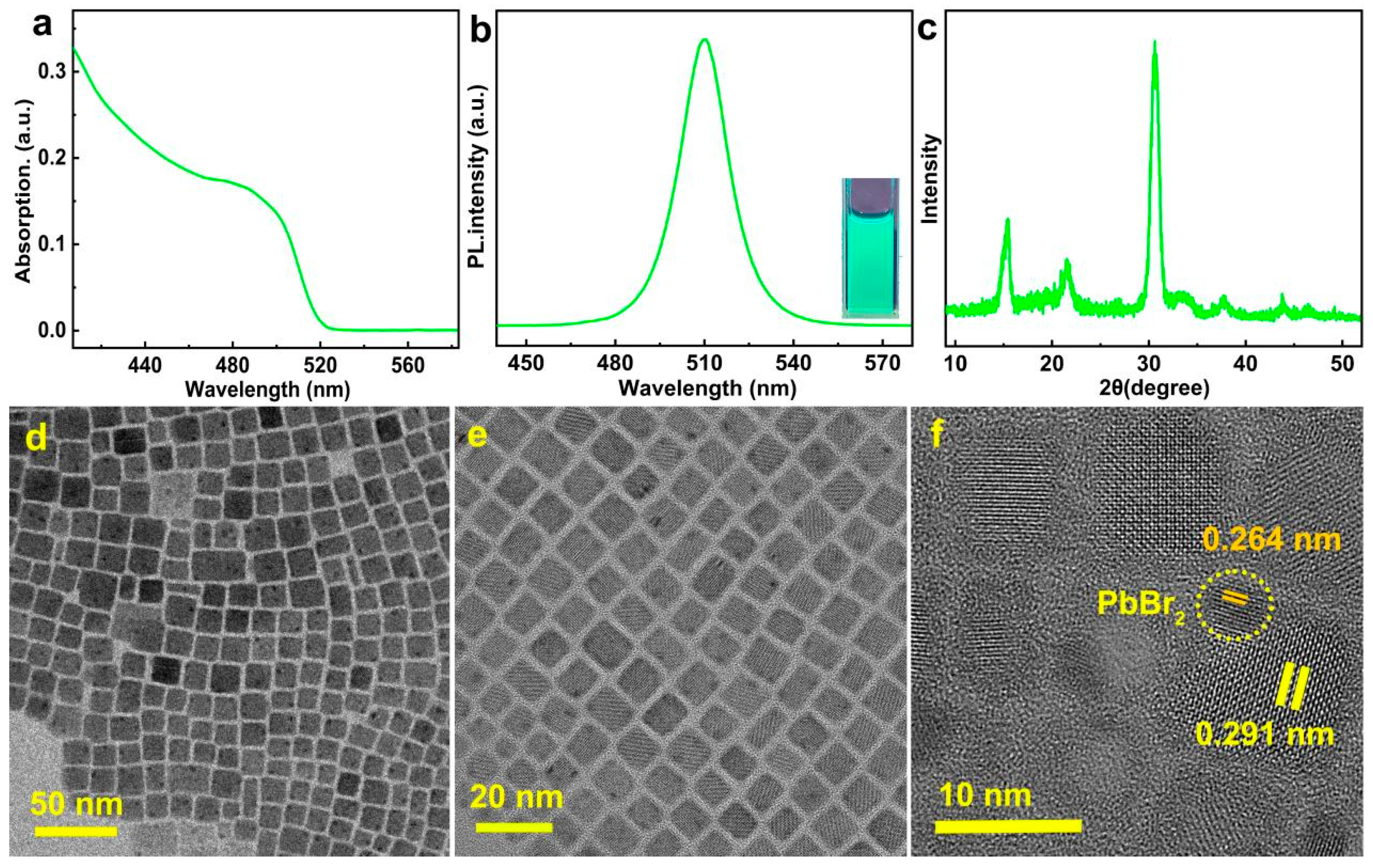
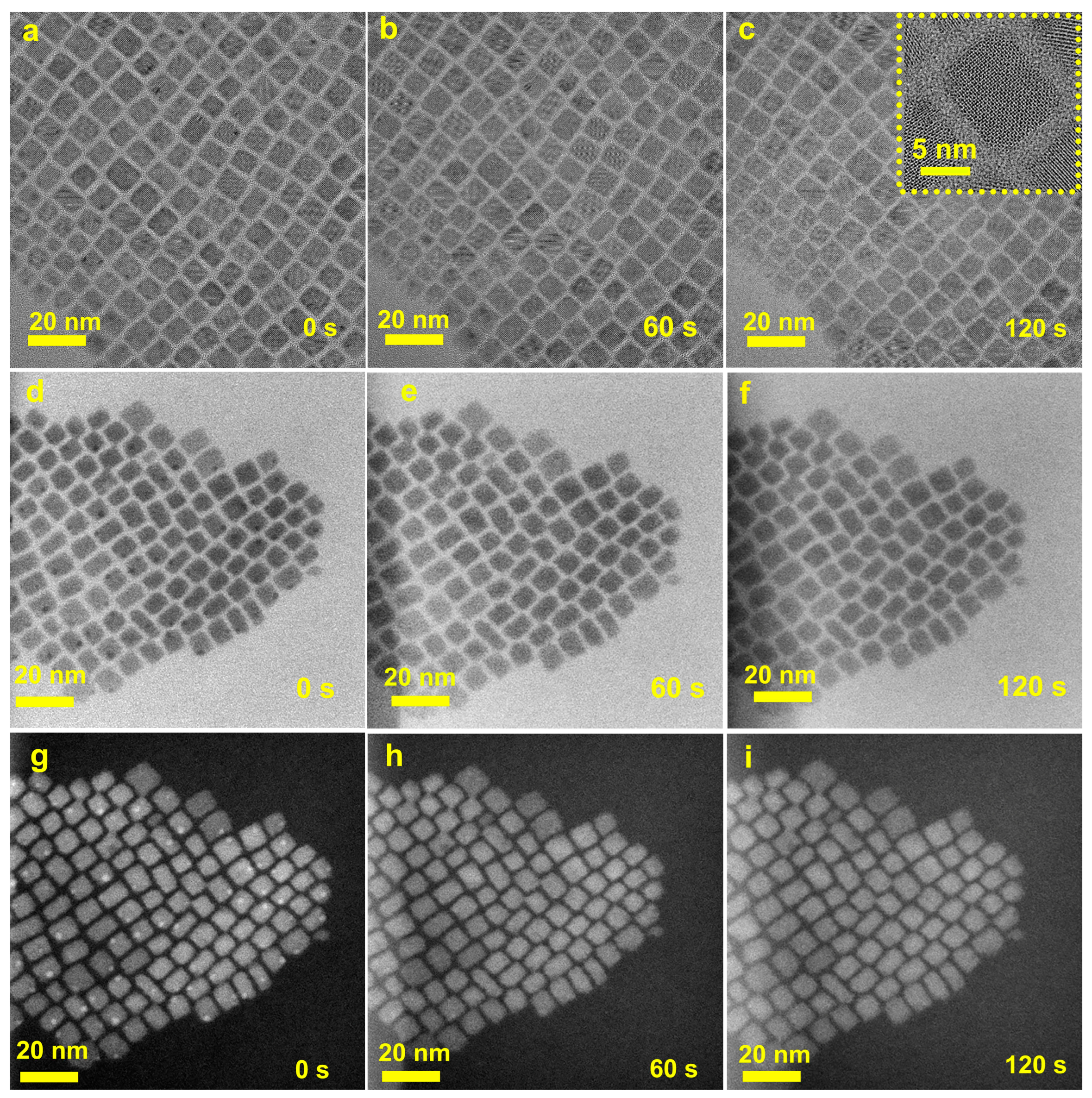
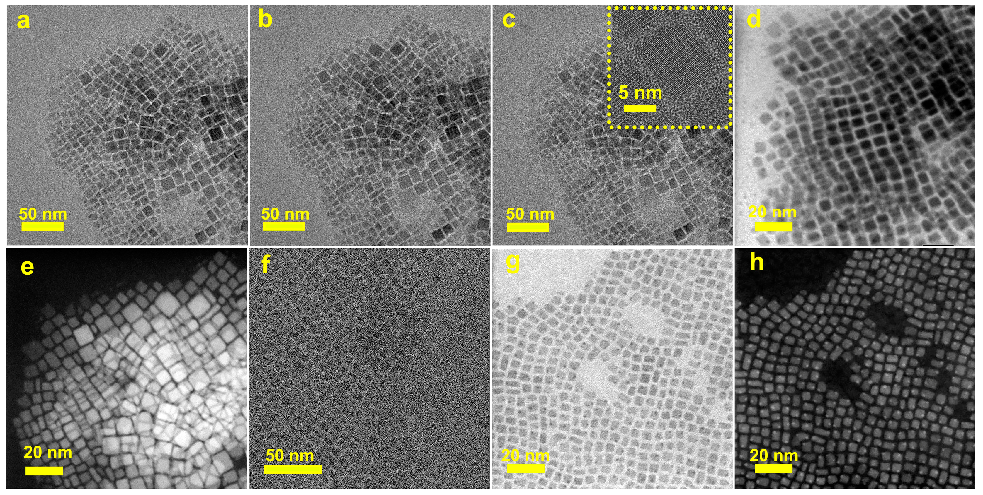
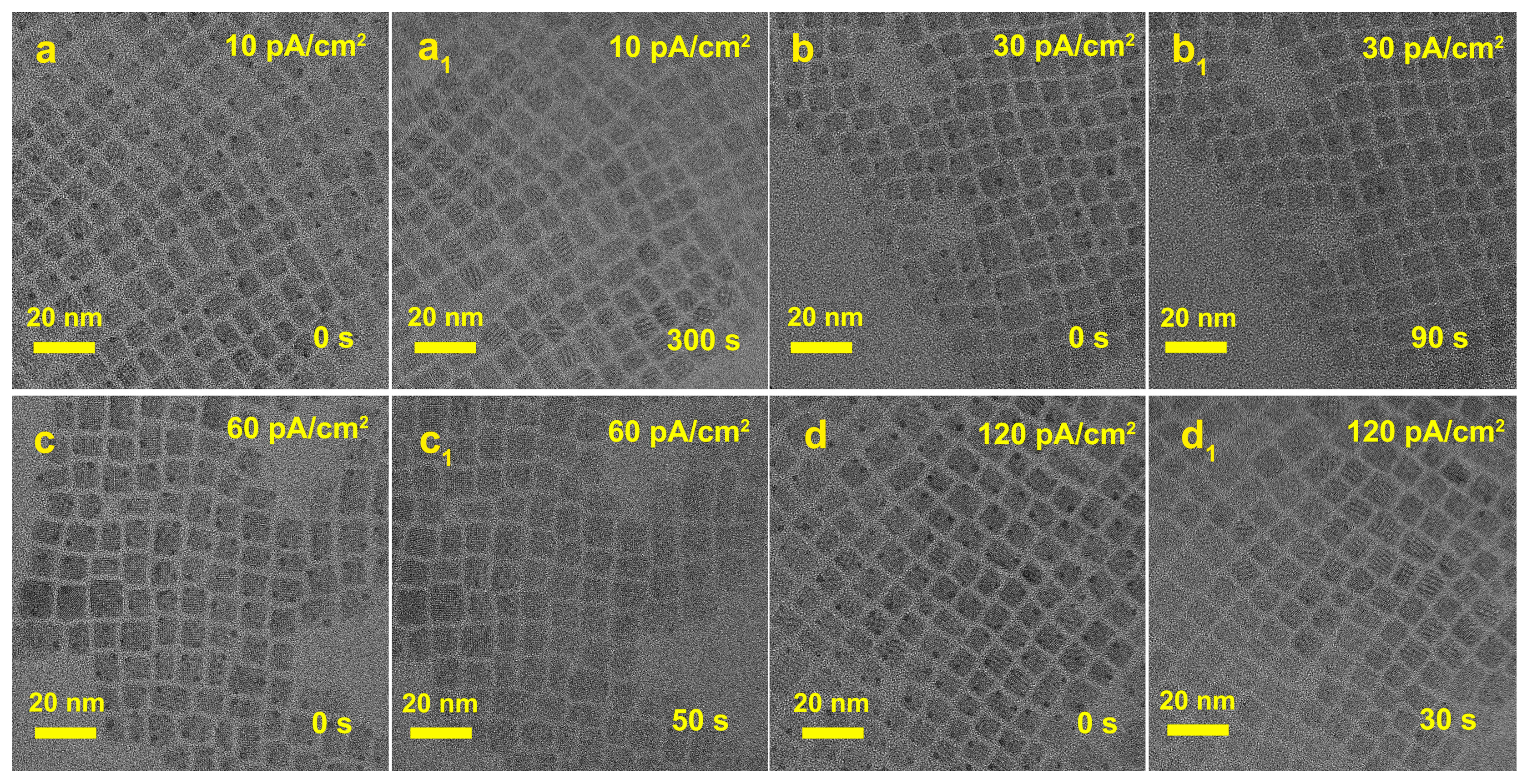
3. Results and Discussion

The green-emission QDs were prepared through the hot-injection method using organic long-chain oleic acid (OA) and oleylamine (OAm) as ligands. As shown in Figure 1, ultraviolet visible (UV-vis) absorption and photoluminescence (PL) were carried out to explore their optical properties. In Figure 1a, UV-vis absorption spectra show that CsPbBr3 QDs have a distinct absorption peak at 485 nm. The steady-state PL image shows that the emission peak of CsPbBr3 QDs is at 510 nm and emits bright green light under 365 nm UV irradiation. It can be proven from the excitation spectrum of the 510 nm band (Figure S1) that the best excitation wavelength is 365 nm. Furthermore, the half-peak width of the QD emission peak was calculated at 19 nm, indicating that the particle size of CsPbBr3 QDs distributed uniformly. The result of X-ray diffraction (XRD) (Figure 1c) showed that three strong diffraction peaks at 14.9°, 21.0°, and 29.9° correspond to the (100), (110) and (200) crystal planes, respectively. The high intensity and sharp peak of the diffraction peaks indicate QDs with good crystal structure.
In order to further investigate the size and morphology of CsPbBr3 QDs, TEM testing was performed (Figure 1d). From the TEM morphology result of CsPbBr3 QDs, it can be seen that the grain size of the QDs is uniform, mostly within the range of 7–11 nm. To provide a more accurate description, 50 randomly selected grains were analyzed for particle size distribution (Figure S2). Over 80% of particles showed a particle size between 7 and 11 nm, with the smallest grain size at around 7 nm and the largest at around 12 nm, and few particle sizes are out of the range 7–11 nm. In Figure 1d,e, it is indicated that there are many “black spots” on the surface of CsPbBr3 QDs measured at about 2 nm. According to our research, these “black spots” are the surface defects of the QDs. Due to the defects were presence on the surface of QDs, this resulted in a low photoluminescence yield (PLQY) of 42.38% (Table S1) for CsPbBr3 QDs. Time-resolved PL (TRPL) was used to further test the lifetime of CsPbBr3 QDs and perform fitting. The TRPL spectrum (Figure S3) shows that the nonradiative recombination lifetime τ2 caused by defects is 5.86 ns, accounting for 51.15%, which indicates that there are many defects on the surface of QDs. High-resolution TEM (HRTEM) testing was performed to further investigate the structure of “black spots”. As shown in Figure 1f, the interplanar spacing of “black spots” is 0.264 nm, corresponding to the (031) plane of the [PbBr6]4− octahedron, which indicates the “black spots” formed by the surface uncoordinated [PbBr6]4− octahedron. The interplanar spacing of 0.291 nm corresponds to the (200) plane of CsPbBr3 QDs.
When we tried to adjust the magnification of the TEM to 200 k, a morphology image of CsPbBr3 QDs was immediately taken, as shown in Figure 2a. There are many “black spots” on the surface of CsPbBr3 QDs formed by [PbBr6]4− octahedron. After radiation for 60 s at this magnification, the morphology image was obtained again (Figure 2b). The TEM result indicated that “black spots” on the surface of QDs were significantly reduced. When the radiation time reached 120 s (Figure 2c), the “black spots” were rarely observed. In order to better present the change process, corresponding recordings were made using screen recording. As observed in the Video S1, the “black spots” on the QD’s surface were very obvious at the beginning of shooting, but after high magnification radiation, the “black spots” slowly decreased until they disappeared completely. It can be attributed to the fact that the electron beam (17 pA/cm2) peeled [PbBr6]4− octahedron from the surface of the QDs to reduce surface defects, resulting in a decrease in “dark spots” on the QDs surface. In order to further verify the hypothesis, scanning transmission electron microscopy bright field (STEM BF) and HAADF tests were performed on the QDs (0.16 nA, camera length 120 mm, probe size 5). Due to the fact that [PbBr6]4− is a heavy element, it appears as “black spots” in STEM BF and “bright spots” under HAADF test conditions. It can be seen from Figure 2d,g that there are many “black spots” or “bright spots” on the surface of the QDs caused by [PbBr6]4− defects. STEM BF and HAADF test results show that as radiation time increases, the “black spots” or “bright spots” gradually decrease (Figure 2e,f,h,i). When the radiation time increases to 120 s, the “black spots” or “bright spots” basically disappear, which is consistent with TEM results (Figure 2).
As shown in Figure 3a–c, a sample region was first selected and subjected to electron beam irradiation for varying durations. Under TEM mode, the defects on the surface of QDs were stripped away, resulting in an improvement in the crystal structure. The sample was subsequently switched to STEM mode for testing. The STEM BF (Figure 3d) and HAADF (Figure 3e) results indicated that there were indeed no under-coordinated [PbBr6]4− deep-level defects on the QDs surface. Furthermore, it is also demonstrated the ability of electron beams to peel away surface defects and obtain perovskites with better crystal structures for clear, high-resolution images. Under conditions of high magnification of the tests, the irradiation of the QDs by an electron beam could cause organic small-molecule ligands to form a layer of “carbonaceous residue” on the sample surface, which may have covered up surface defects and consequently affected sample observation. In order to avoid interference from this carbonaceous residue, a method of treating the perovskite sample with a surface deposition of an amorphous carbon film (15–20 nm) was used before TEM and HAADF characterization. Note that the defects are not covered up by the layer of amorphous carbon film deposited on the QDs surface, as we can clearly observe the defects on the surface of the QDs from the test results (Figure 3f–h) caused by under-coordinated [PbBr6]4−. It was further confirmed that the disappearance of defects is attributed to the stripping effect of the electron beam. In order to elaborate on the underlying mechanisms causing the observed morphological variations, the difference current density of the electron beam was used to obtain TEM images of QDs. As shown in Figure 4, the time for [PbBr6]4− octahedron defects to be completely peeled from the QD’s surface becomes shorter (from 300 s to 30 s) with the electron beam current density increasing from 10 to 120 pA/cm2. It indicated that the coordination interaction with Cs and [PbBr6]4− octahedron was more easily dissociated when the energy of the electron beam was increased.

4. Conclusions

In this work, a novel method was proposed using electron beam irradiation to remove surface defects from QDs and obtain clear, high-resolution images. Typically, when QDs are synthesized by the method of hot injection, uncoordinated Pb vacancy defects will form on the surface, which can affect the analysis of the QDs crystal structure. TEM and HAADF results indicated that the [PbBr6]4− octahedron could be removed from the surface of the QDs when the beam energy is stronger than the binding energy between Cs and [PbBr6]4−. Thereby, complete crystal information for CsPbBr3 QDs was obtained by avoiding the interference of defects in the crystal structure. This method provides a new approach to preprocess sensitive crystalline materials and analyze their atomic-scale structure and chemical properties by using the irradiation energy of electron beams.

Supplementary Materials

The following supporting information can be downloaded at: https://www.mdpi.com/article/10.3390/ma16176010/s1. Figure S1: The excitation spectrum of the 510 nm band; Figure S2: The grain size of 50 CsPbBr3 QDs grains were collected for each group; Figure S3: The TRPL of CsPbBr3 QDs; Table S1: Optical parameters of CsPbBr3 QDs.

Author Contributions

Conceptualization, L.Y. and T.Z.; Formal analysis and writing—original draft, Y.L.; Investigation, W.Y., F.J. and A.Z.; Methodology and visualization, G.L.; Writing—review and editing, G.L. All authors have read and agreed to the published version of the manuscript.

Funding

This research received no external funding.

Institutional Review Board Statement

Not applicable.

Informed Consent Statement

Not applicable.

Data Availability Statement

All data included in this study are available upon request by contacting the corresponding authors.

Acknowledgments

The author would like to thank Yaxin Li, Tianjin University for his advice and assistance in this work.

Conflicts of Interest

The authors declare no conflict of interest.

References

  1. Swarnkar, A.; Chulliyil, R.; Ravi, V.K.; Irfanullah, M.; Chowdhury, A.; Nag, A. Colloidal CsPbBr3 Perovskite Nanocrystals: Luminescence beyond Traditional Quantum Dots. Angew. Chem. Int. Ed. 2015, 54, 15424–15428. [Google Scholar] [CrossRef]
  2. Protesescu, L.; Yakunin, S.; Bodnarchuk, M.I.; Krieg, F.; Caputo, R.; Hendon, C.H.; Yang, R.X.; Walsh, A.; Kovalenko, M.V. Nanocrystals of Cesium Lead Halide Perovskites (CsPbX3, X=Cl, Br, and I): Novel Optoelectronic Materials Showing Bright Emission with Wide Color Gamut. Nano Lett. 2015, 15, 3692–3696. [Google Scholar] [CrossRef] [PubMed]
  3. Li, X.; Wu, Y.; Zhang, S.; Cai, B.; Gu, Y.; Song, J.; Zeng, H. CsPbX3 Quantum Dots for Lighting and Displays: Room Temperature Synthesis, Photoluminescence Superiorities, Underlying Origins and White Light-Emitting Diodes. Adv. Funct. Mater. 2016, 26, 2435–2445. [Google Scholar] [CrossRef]
  4. Kovalenko, M.V.; Protesescu, L.; Bodnarchuk, M.I. Properties and potential optoelectronic applications of lead halide perovskite nanocrystals. Science 2017, 358, 745–750. [Google Scholar] [CrossRef]
  5. Lin, K.; Xing, J.; Quan, L.N.; De Arquer, F.P.G.; Gong, X.; Lu, J.; Xie, L.; Zhao, W.; Zhang, D.; Yan, C.; et al. Perovskite light-emitting diodes with external quantum efficiency exceeding 20 per cent. Nature 2018, 562, 245–248. [Google Scholar] [CrossRef] [PubMed]
  6. Tan, Z.K.; Moghaddam, R.S.; Lai, M.L.; Docampo, P.; Higler, R.; Deschler, F.; Price, M.B.; Sadhanala, A.; Pazos-Outon, L.M.; Credgington, D.; et al. Bright light-emitting diodes based on organometal halide perovskite. Nat. Nanotechnol. 2014, 9, 687–692. [Google Scholar] [CrossRef] [PubMed]
  7. Chiba, T.; Hoshi, K.; Pu, Y.-J.; Takeda, Y.; Hayashi, Y.; Ohisa, S.; Kawata, S.; Kido, J. High-Efficiency Perovskite Quantum-Dot Light-Emitting Devices by Effective Washing Process and Interfacial Energy Level Alignment. ACS Appl. Mater. Interfaces 2017, 9, 18054–18060. [Google Scholar] [CrossRef]
  8. Kim, H.-S.; Lee, C.-R.; Im, J.-H.; Lee, K.-B.; Moehl, T.; Marchioro, A.; Moon, S.-J.; Humphry-Baker, R.; Yum, J.-H.; Moser, J.E.; et al. Lead Iodide Perovskite Sensitized All-Solid-State Submicron Thin Film Mesoscopic Solar Cell with Efficiency Exceeding 9%. Sci. Rep. 2012, 2, 591. [Google Scholar] [CrossRef]
  9. Yang, K.; Li, F.; Liu, Y.; Xu, Z.; Li, Q.; Sun, K.; Qiu, L.; Zeng, Q.; Chen, Z.; Chen, W.; et al. All-Solution-Processed Perovskite Quantum Dots Light-Emitting Diodes Based on the Solvent Engineering Strategy. ACS Appl. Mater. Interfaces 2018, 10, 27374–27380. [Google Scholar] [CrossRef]
  10. Lu, C.H.; Biesold-McGee, G.V.; Liu, Y.; Kang, Z.; Lin, Z. Doping and ion substitution in colloidal metal halide perovskite nanocrystals. Chem. Soc. Rev. 2020, 49, 4953–5007. [Google Scholar] [CrossRef] [PubMed]
  11. Jabeen, N.; Zaidi, A.; Hussain, A.; Hassan, N.U.; Ali, J.; Ahmed, F.; Khan, M.U.; Iqbal, N.; Elnasr, T.A.S.; Helal, M.H. Single-and Multilayered Perovskite Thin Films for Photovoltaic Applictions. Nanomaterials 2022, 12, 3208. [Google Scholar] [CrossRef] [PubMed]
  12. Kuimalee, S.; Chairuangsri, T.; Pearce, J.T.; Edmonds, D.V.; Brown, A.P.; Brydson, R.M. Quantitative analysis of a complex metal carbide formed during furnace cooling of cast duplex stainless steel using EELS and EDS in the TEM. Micron 2010, 41, 423–429. [Google Scholar] [CrossRef] [PubMed]
  13. Zhang, S.; Liu, C.; Wang, H.; Wang, H.; Sun, J.; Zhang, Y.; Han, X.; Cao, Y.; Liu, S.; Sun, J. A Covalent P–C Bond Stabilizes Red Phosphorus in an Engineered Carbon Host for High-Performance Lithium-Ion Battery Anodes. ACS Nano 2021, 15, 3365–3375. [Google Scholar] [CrossRef] [PubMed]
  14. Susi, T.; Kotakoski, J.; Arenal, R.; Kurasch, S.; Jiang, H.; Skakalova, V.; Stephan, O.; Krasheninnikov, A.V.; Kauppinen, E.I.; Kaiser, U.; et al. Atomistic Description of Electron Beam Damage in Nitrogen-Doped Graphene and Single-Walled Carbon Nanotubes. ACS Nano 2012, 6, 8837–8846. [Google Scholar] [CrossRef] [PubMed]
  15. Egerton, R. Mechanisms of radiation damage in beam-sensitive specimens, for TEM accelerating voltages between 10 and 300 kV. Microsc. Res. Tech. 2012, 75, 1550–1556. [Google Scholar] [CrossRef]
  16. Bell, D.C.; Mankin, M.; Day, R.W.; Erdman, N. Natasha Erdman, Successful application of Low Voltage Electron Microscopy to practical materials problems. Ultramicroscopy 2014, 145, 56–65. [Google Scholar] [CrossRef]
  17. Mastrikov, Y.A.; Chuklina, N.G.; Sokolov, M.N.; Popov, A.I.; Gryaznov, D.V.; Kotomin, E.A.; Maier, J. Small radius electron and hole polarons in PbX2 (X=F, Cl, Br) crystals: A computational study. J. Mater. Chem. C 2021, 9, 16536–16544. [Google Scholar] [CrossRef]
  18. Reichling, M.; Wilson, R.; Bennewitz, R.; Williams, R.; Gogoll, S.; Stenzel, E.; Matthias, E. Surface colloid evolution during low-energy electron irradiation of CaF2(111). Surf. Sci. 1996, 366, 531–544. [Google Scholar] [CrossRef]
  19. Postawa, Z.; Kolodziej, J.; Baran, G.; Czuba, P.; Piatkowski, P.; Szymonski, M.; Plavina, I.; Popov, A. ESD of nonthermal halogen atoms from In-doped (001) KBr. Nucl. Instrum. Methods Phys. Res. Sect. B Beam Interact. Mater. At. 1995, 100, 228–231. [Google Scholar] [CrossRef]
  20. Zhang, D.; Zhu, Y.; Liu, L.; Ying, X.; Hsiung, C.-E.; Sougrat, R.; Li, K.; Han, Y. Atomic-resolution transmission electron microscopy of electron beam–sensitive crystalline materials. Science 2018, 359, 675–679. [Google Scholar] [CrossRef]
  21. Liu, Y.; Ju, Z.; Zhang, B.; Wang, Y.; Nai, J.; Liu, T.; Tao, X. Visualizing the Sensitive Lithium with Atomic Precision: Cryogenic Electron Microscopy for Batteries. Accounts Chem. Res. 2021, 54, 2088–2099. [Google Scholar] [CrossRef] [PubMed]
  22. Meyer, J.C.; Kotakoski, J.; Mangler, C. Atomic structure from large-area, low-dose exposures of materials: A new route to circum-vent radiation damage. Ultramicroscopy 2014, 145, 13–21. [Google Scholar] [CrossRef] [PubMed]
  23. Jia, C.L.; Lentzen, M.; Urban, K. Atomic-Resolution Imaging of Oxygen in Perovskite Ceramics. Science 2003, 299, 870–873. [Google Scholar] [CrossRef]
  24. Yu, Y.; Zhang, D.; Kisielowski, C.; Dou, L.; Kornienko, N.; Bekenstein, Y.; Wong, A.B.; Alivisatos, A.P.; Yang, P. Atomic Resolution Imaging of Halide Perovskites. Nano Lett. 2016, 16, 7530–7535. [Google Scholar] [CrossRef] [PubMed]
  25. dos Reis, R.; Yang, H.; Ophus, C.; Ercius, P.; Bizarri, G.; Perrodin, D.; Shalapska, T.; Bourret, E.; Ciston, J.; Dahmen, U. Determination of the structural phase and octahedral rotation angle in halide perovskites. Appl. Phys. Lett. 2018, 112, 071901. [Google Scholar] [CrossRef]
  26. Li, Y.; Zhou, W.; Li, Y.; Huang, W.; Zhang, Z.; Chen, G.; Wang, H.; Wu, G.-H.; Rolston, N.; Vila, R.; et al. Unravelling degradation mechanisms and atomic structure of organic-inorganic halide perovskites by cryo-EM. Joule 2019, 3, 2854–2866. [Google Scholar] [CrossRef]
  27. Cai, S.; Dai, J.; Shao, Z.; Rothmann, M.U.; Jia, Y.; Gao, C.; Hao, M.; Pang, S.; Wang, P.; Lau, S.P.; et al. Atomically resolved electrically active intragrain interfaces in perovskite semiconductors. J. Am. Chem. Soc. 2022, 144, 1910–1920. [Google Scholar] [CrossRef]
  28. Nann, T.; Skinner, W.M. Quantum Dots for Electro-Optic Devices. Acs Nano 2011, 5, 5291–5295. [Google Scholar] [CrossRef]
  29. Li, H.; Xiao, H.-J.; Zhu, T.-S.; Xuan, H.-C.; Li, M. Size Consideration on Shape Factor and Its Determination Role on the Thermodynamic Stability of Quantum Dots. J. Phys. Chem. C 2015, 119, 12002–12007. [Google Scholar] [CrossRef]
  30. Xing, J.; Yan, F.; Zhao, Y.; Chen, S.; Yu, H.; Zhang, Q.; Zeng, R.; Demir, H.V.; Sun, X.; Huan, A.; et al. High-Efficiency Light-Emitting Diodes of Organometal Halide Perovskite Amorphous Nano-particles. ACS Nano 2016, 10, 6623–6630. [Google Scholar] [CrossRef]
  31. Ju, S.; Mao, C.; Zheng, J.; Yang, K.; Lin, L.; Guo, T.; Hu, H.; Li, F. Perovskite Quantum Dot Light-Emitting Memcapacitor. ACS Appl. Nano Mater. 2023, 6, 9219–9225. [Google Scholar] [CrossRef]
  32. Ren, J.; Meijerink, A.; Zhou, X.; Wu, J.; Zhang, G.; Wang, Y. In Situ Embedding Synthesis of CsP-bBr3@Ce-MOF@SiO2 Nanocomposites for High Efficiency Light-Emitting Diodes: Suppressing Reabsorption Losses through the Waveguiding Effect. ACS Appl. Mater. Interfaces 2022, 14, 3176–3188. [Google Scholar] [CrossRef] [PubMed]
Figure 1. (a) UV-visible absorption spectroscopy; (b) PL spectroscopy (inset is a luminescence photograph under a 365 nm UV lamp); (c) X-ray diffraction; (d,e) TEM pictures in different multiples; (f) HRTEM of CsPbBr3 QDs.
Materials 16 06010 g001
Figure 2. (ac) TEM (the insets in (c) is the HRTEM image of CsPbBr3 QDs), STEM BF (df), and HAADF (gi) images of CsPbBr3 QDs after exposure to electron beam irradiation for varying durations.
Materials 16 06010 g002
Figure 3. (ac) The TEM images of CsPbBr3 QDs after exposure to electron beam irradiation for varying durations (the insets in (c) is the HRTEM image of CsPbBr3 QDs); (d,e) respectively show the STEM BF and HAADF images of the sample in figure (a); the TEM (f), STEM BF (g), and HAADF (h) CsPbBr3 QDs were deposited with a layer of amorphous carbon.
Materials 16 06010 g003
Figure 4. TEM images of CsPbBr3 QDs after exposure to electron beam irradiation for varying durations with different beam current densities (a,a1) 10 pA/cm2, (b,b1) 30 pA/cm2, (c,c1) 60 pA/cm2, (d,d1) 120 pA/cm2.
Materials 16 06010 g004
Disclaimer/Publisher’s Note: The statements, opinions and data contained in all publications are solely those of the individual author(s) and contributor(s) and not of MDPI and/or the editor(s). MDPI and/or the editor(s) disclaim responsibility for any injury to people or property resulting from any ideas, methods, instructions or products referred to in the content.

