
Metal Oxide Nanowires Grown by a Vapor–Liquid–Solid Growth Mechanism for Resistive Gas-Sensing Applications: An Overview

 , and
, and
Abstract
:1. Introduction
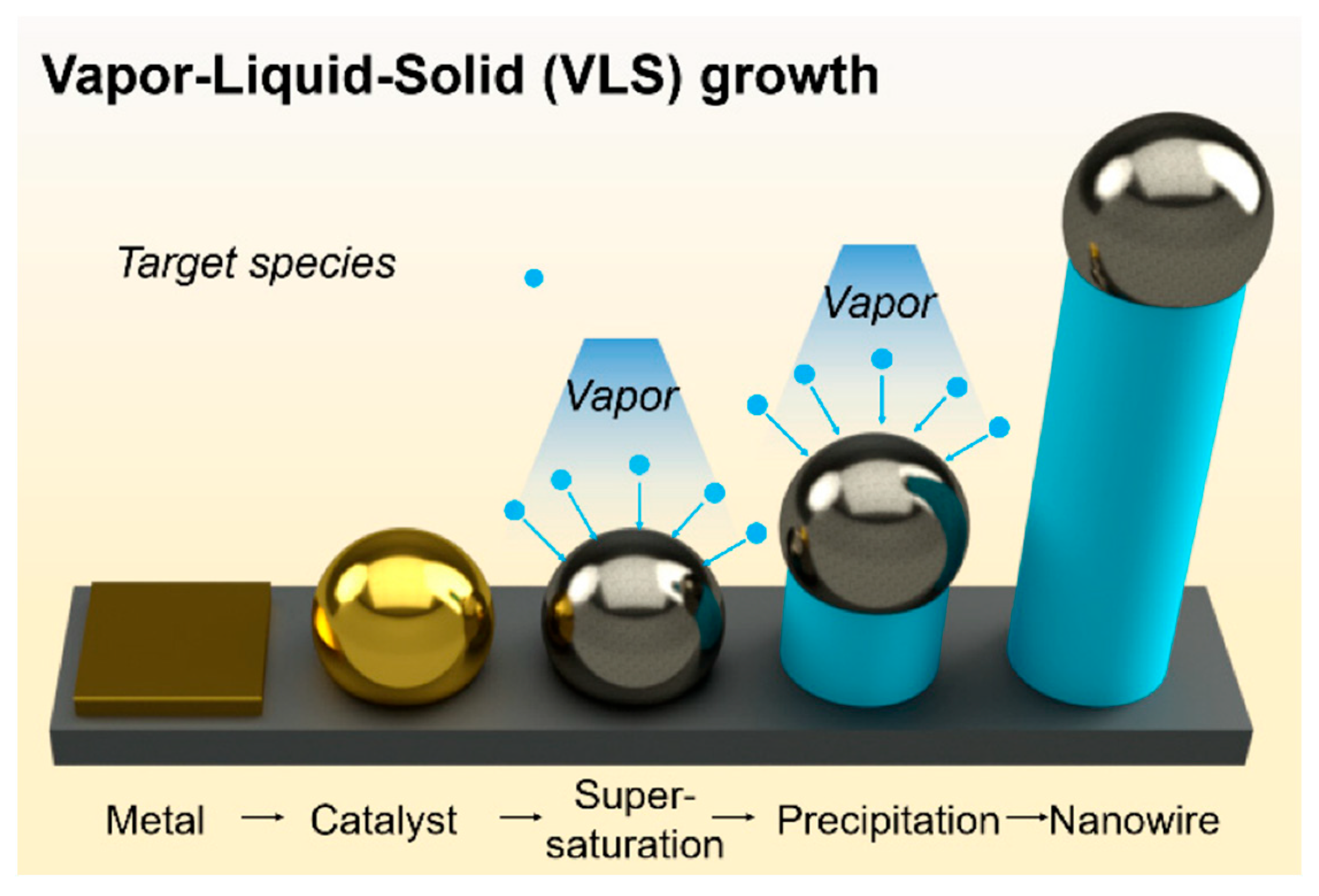
2. VLS Growth Mechanism and Fundamentals
2.1. Metal Catalyst
2.2. Effect of Deposition Temperature
2.3. Effect of the Deposition Pressure
2.4. Effect of the Oxygen Gas Flow
3. VLS-Grown Metal Oxide NWs for Gas-Sensing Studies
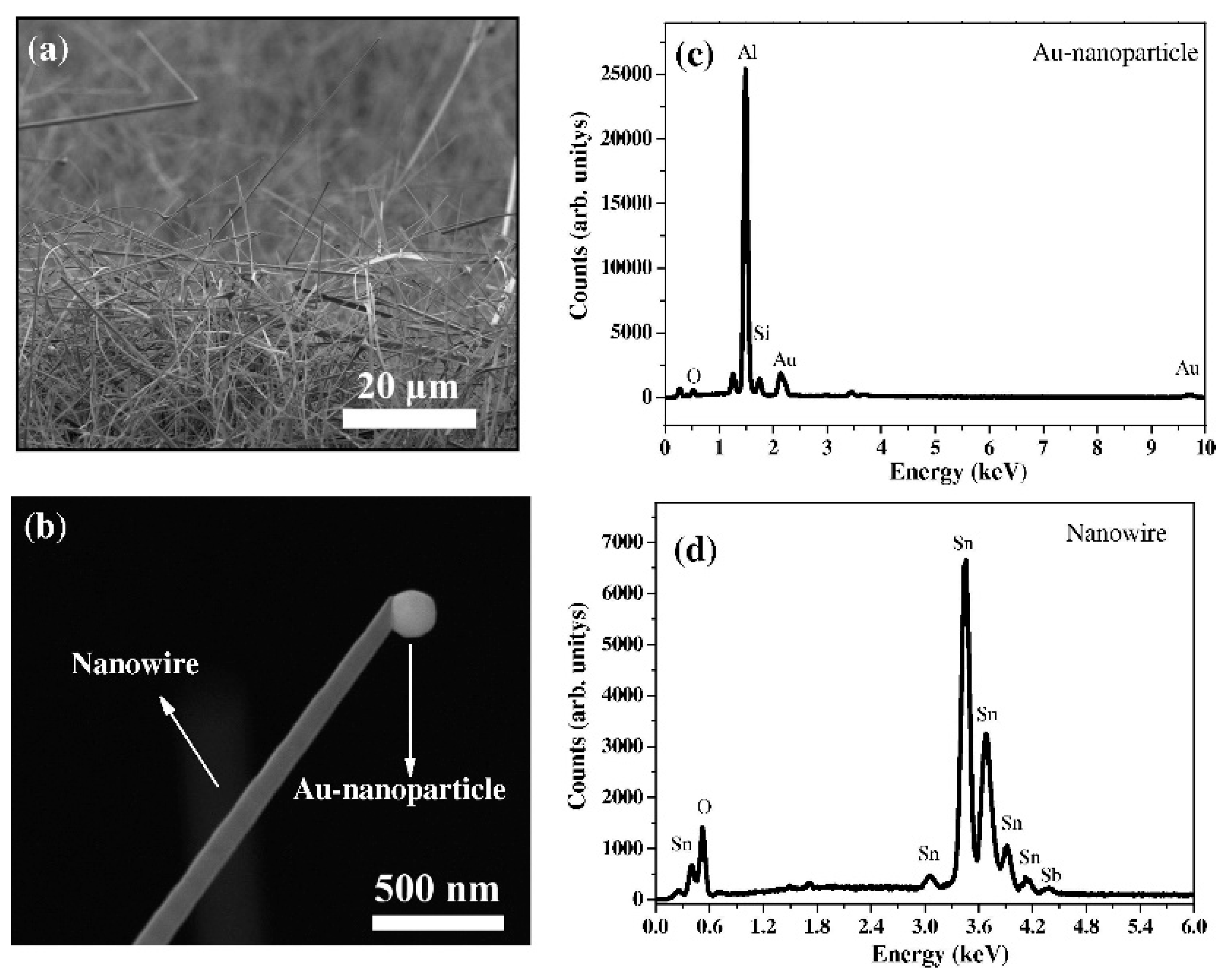
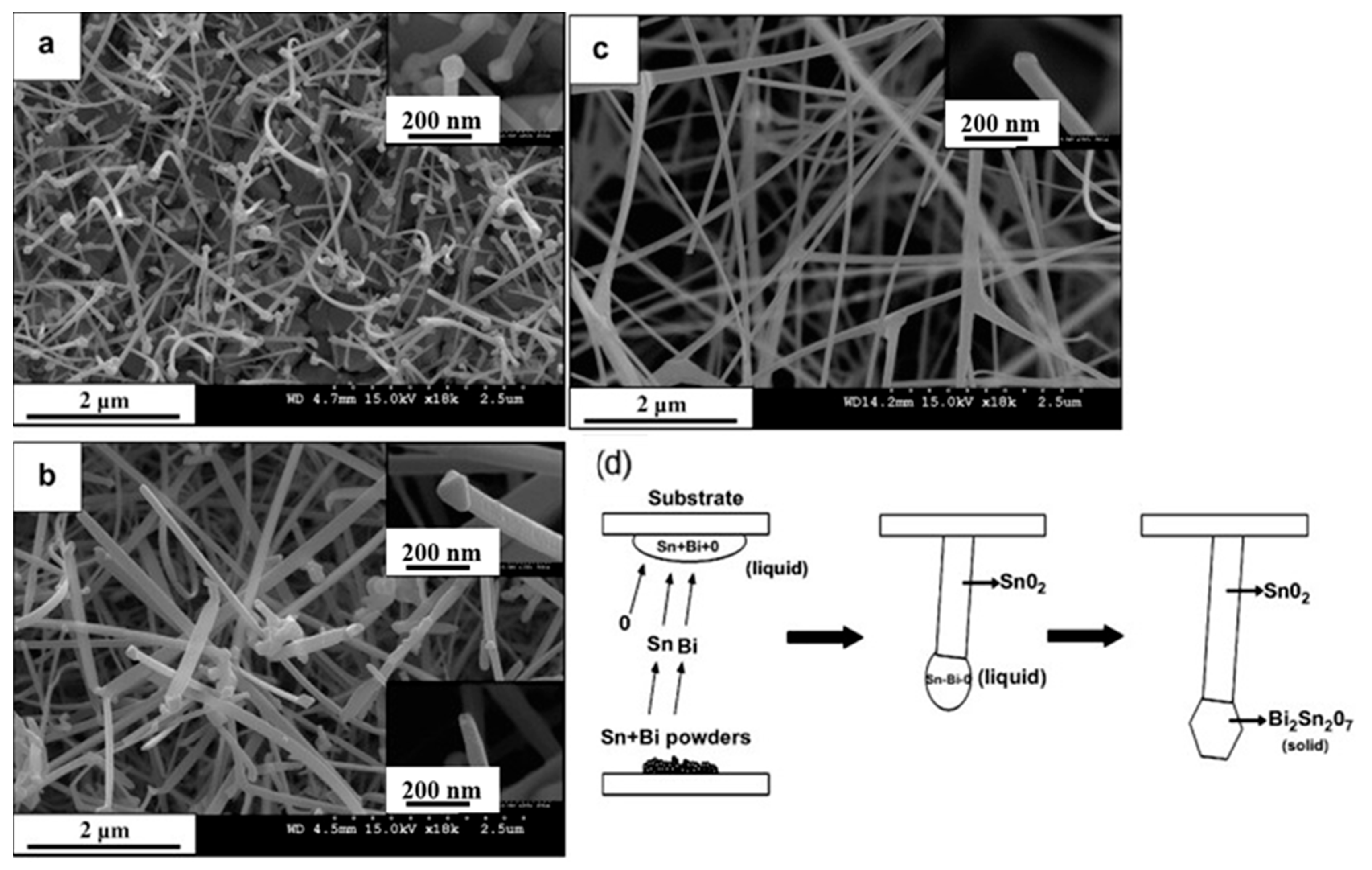
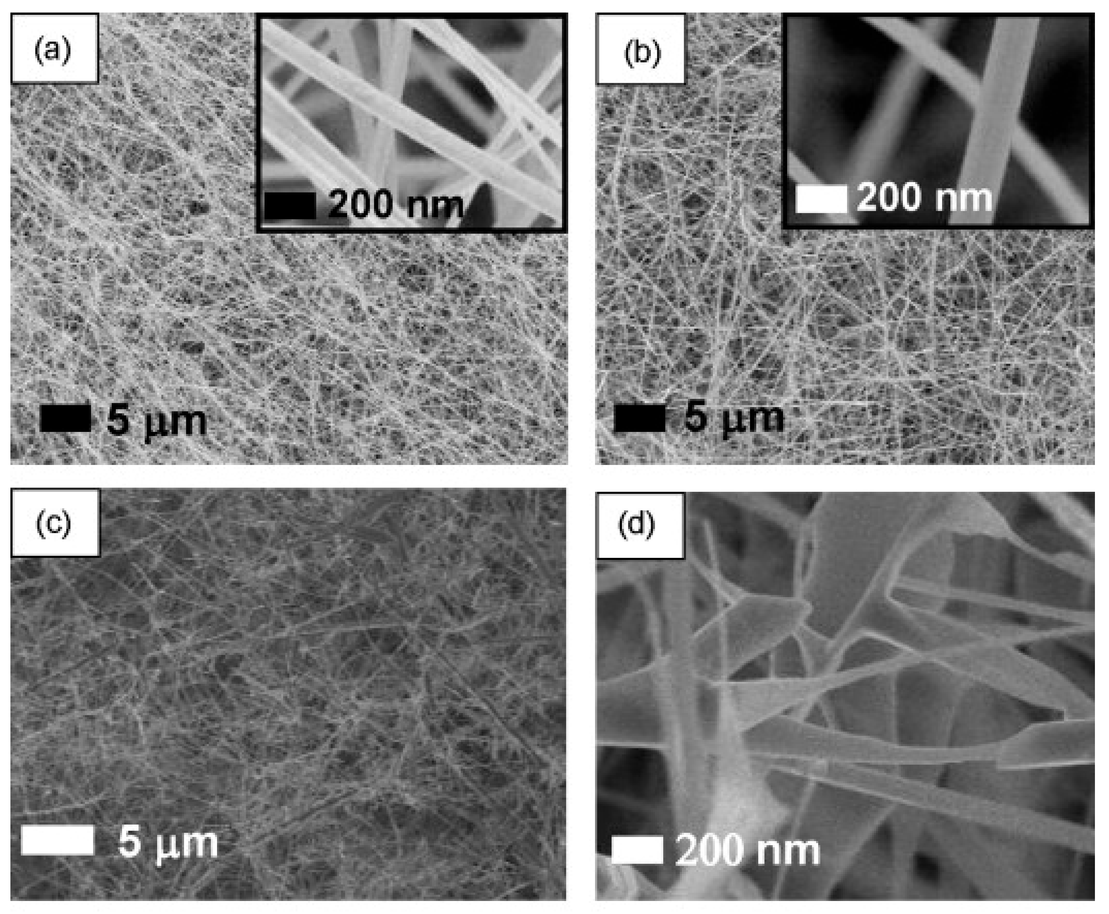
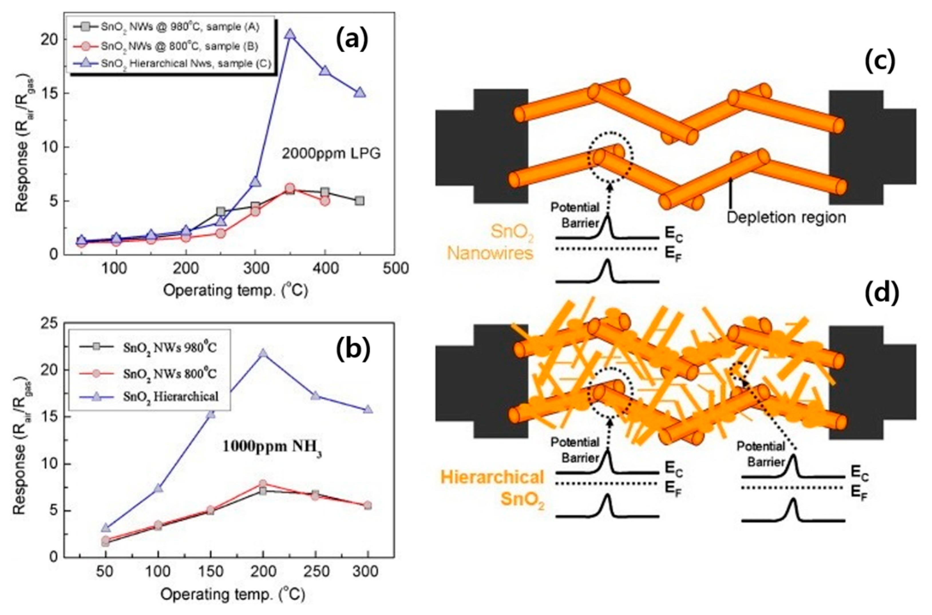
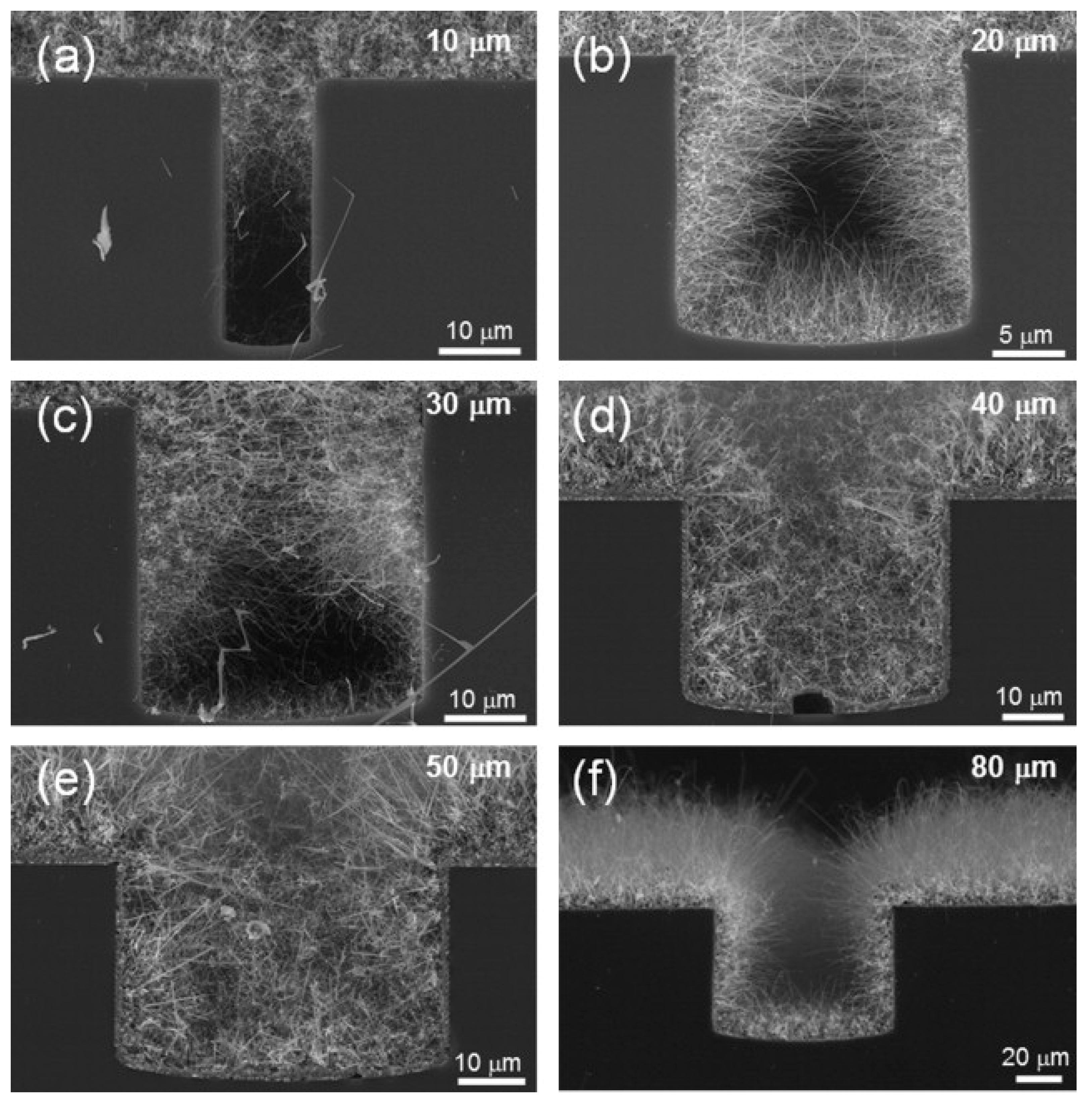
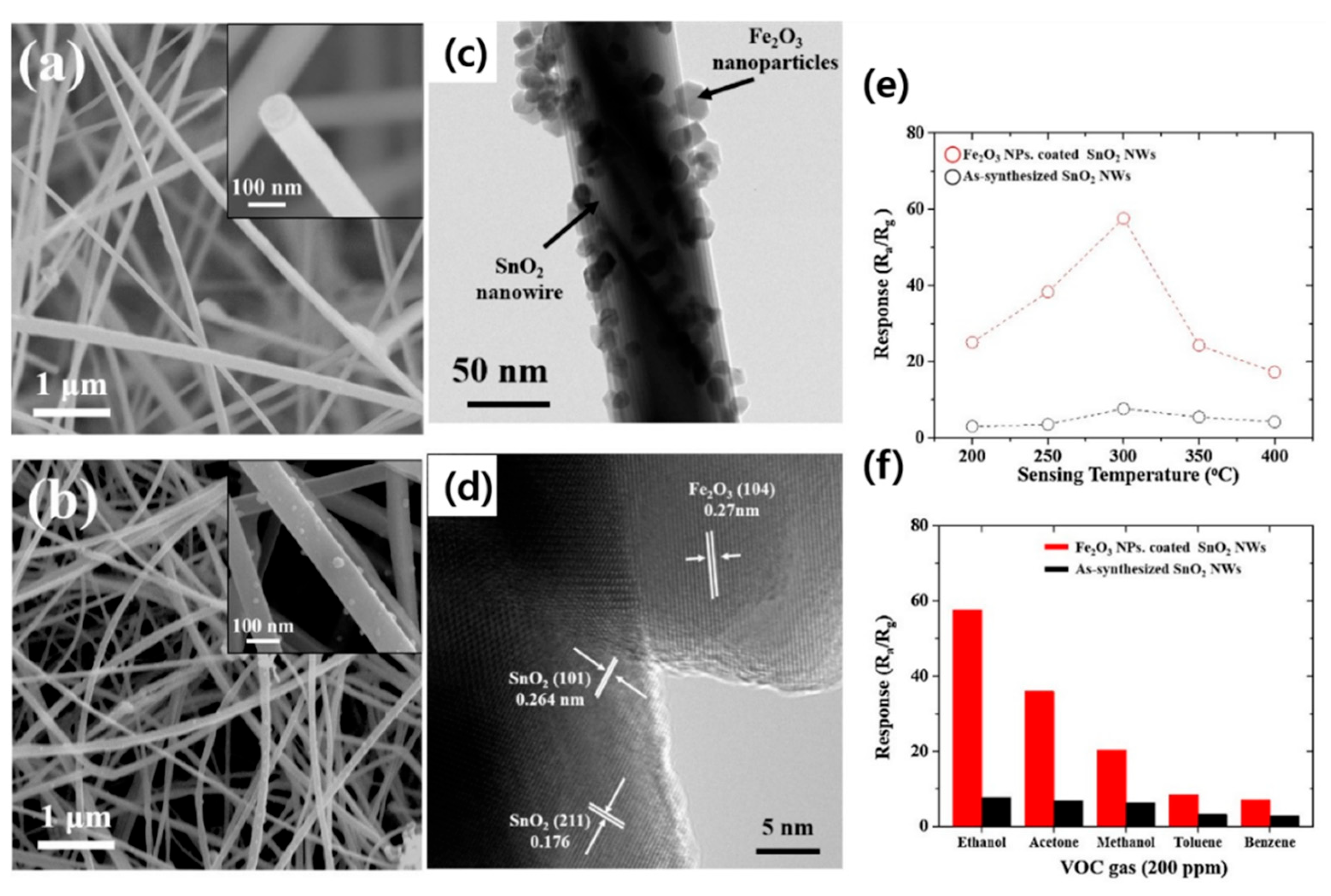
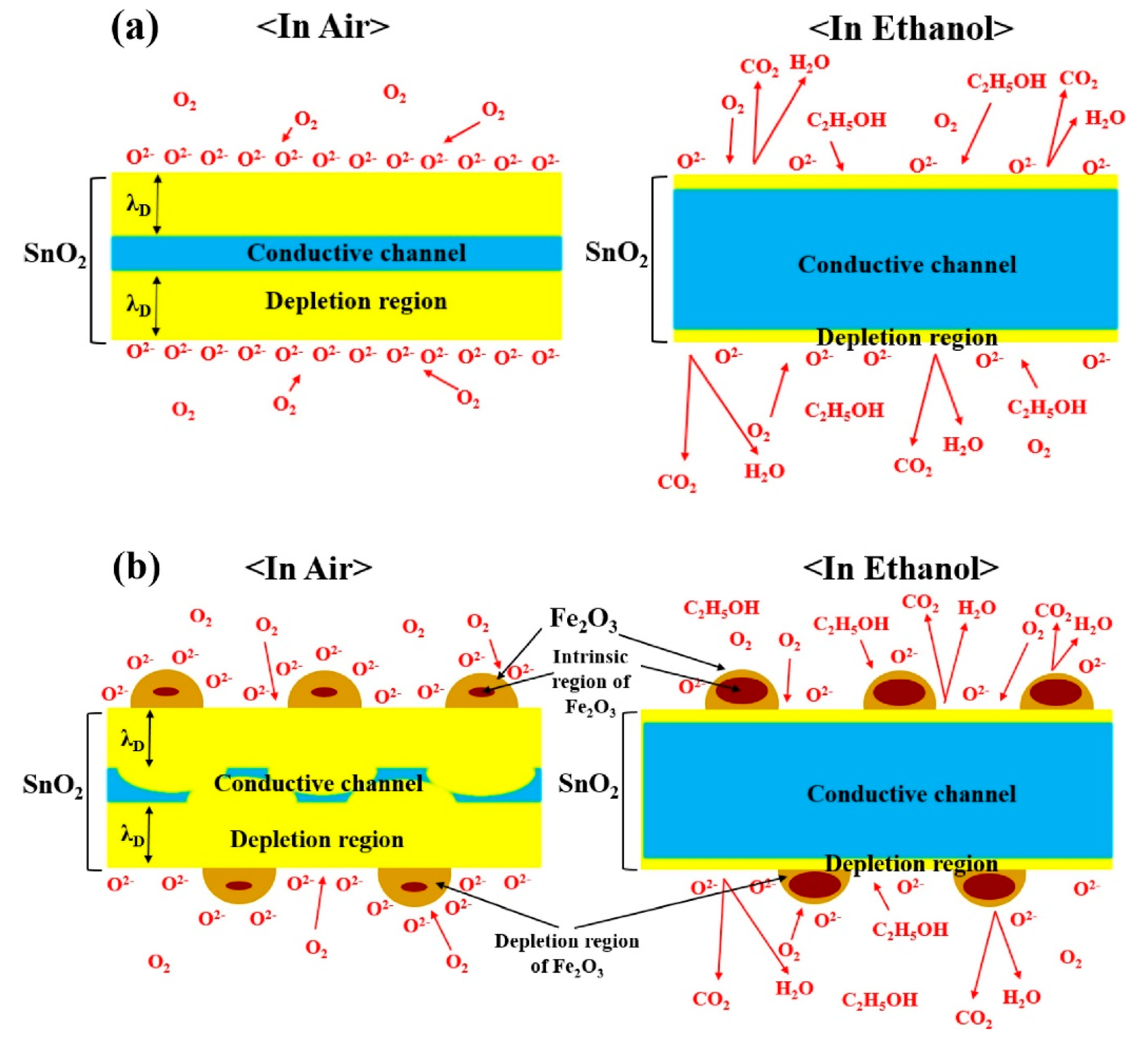
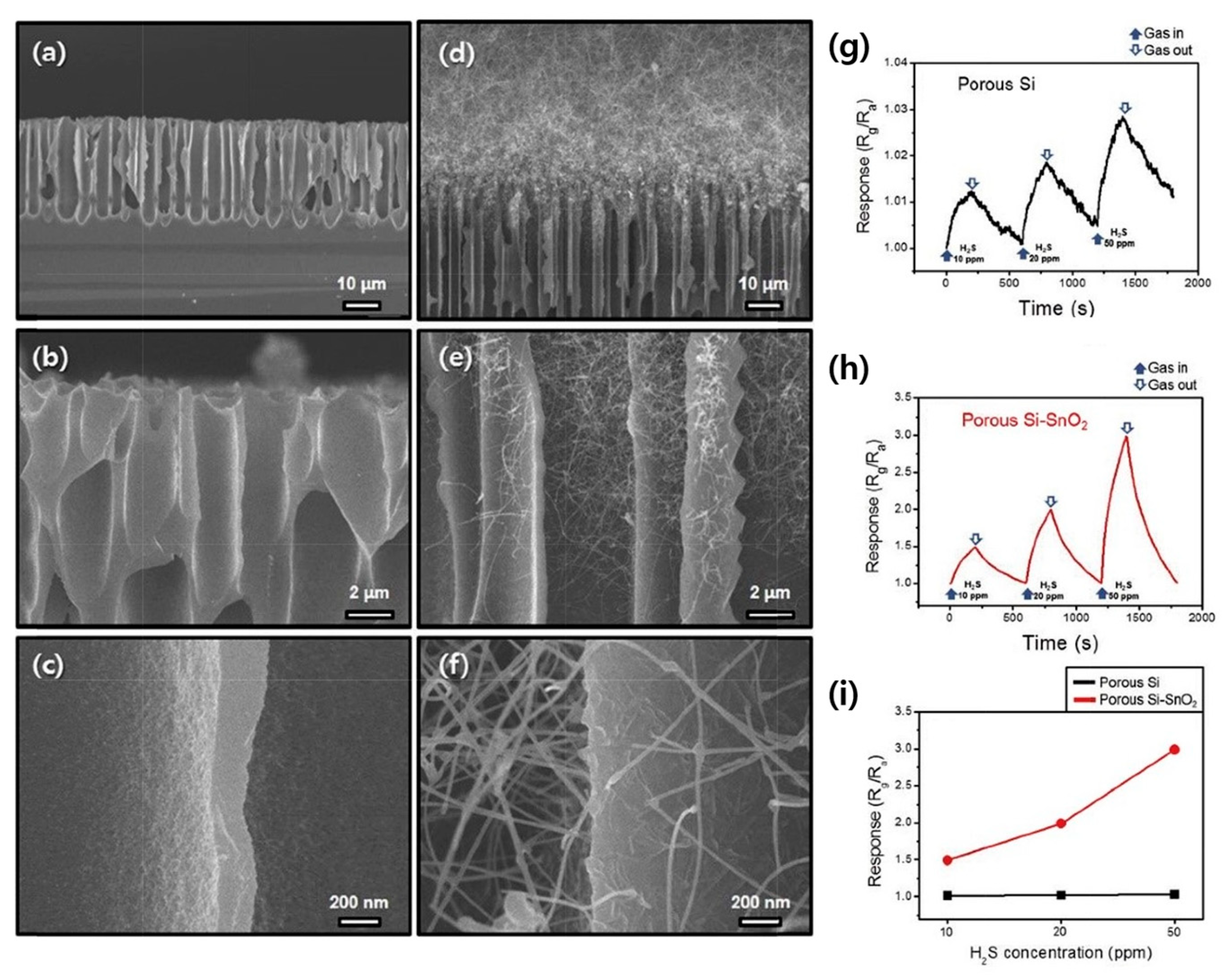
3.1. SnO2 NWs
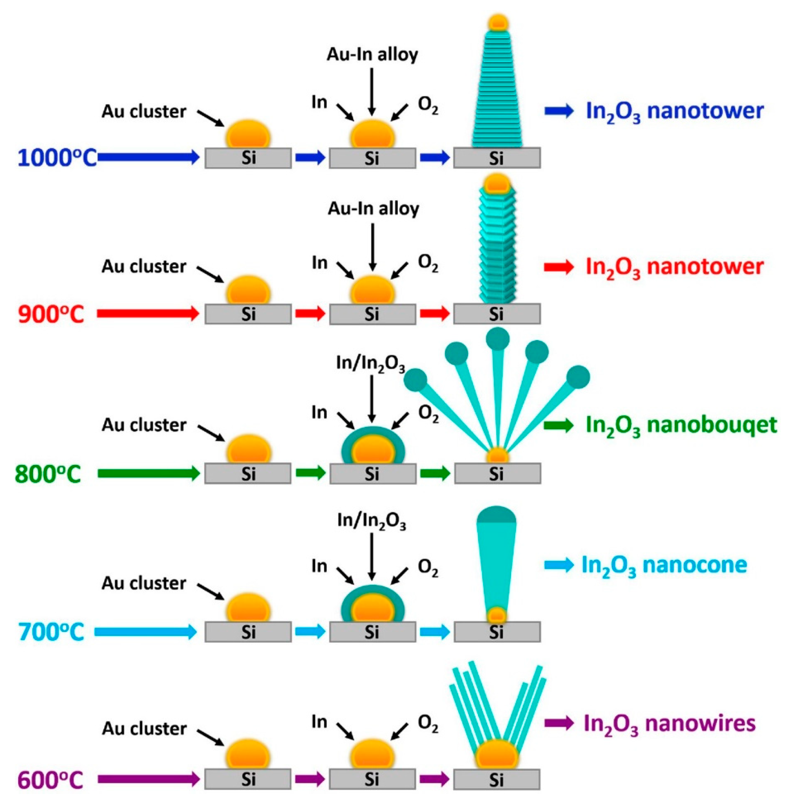
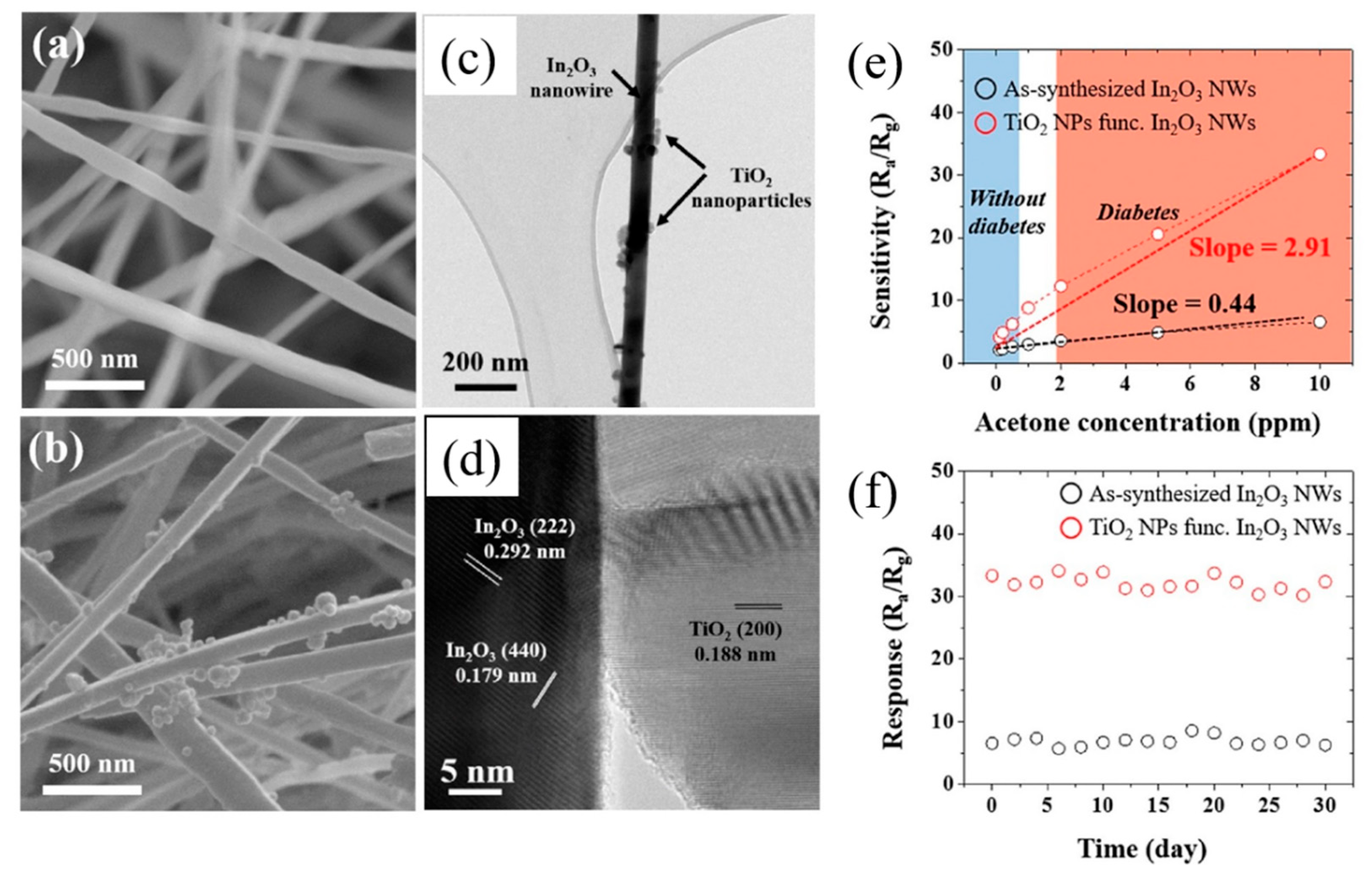
3.2. In2O3 NWs
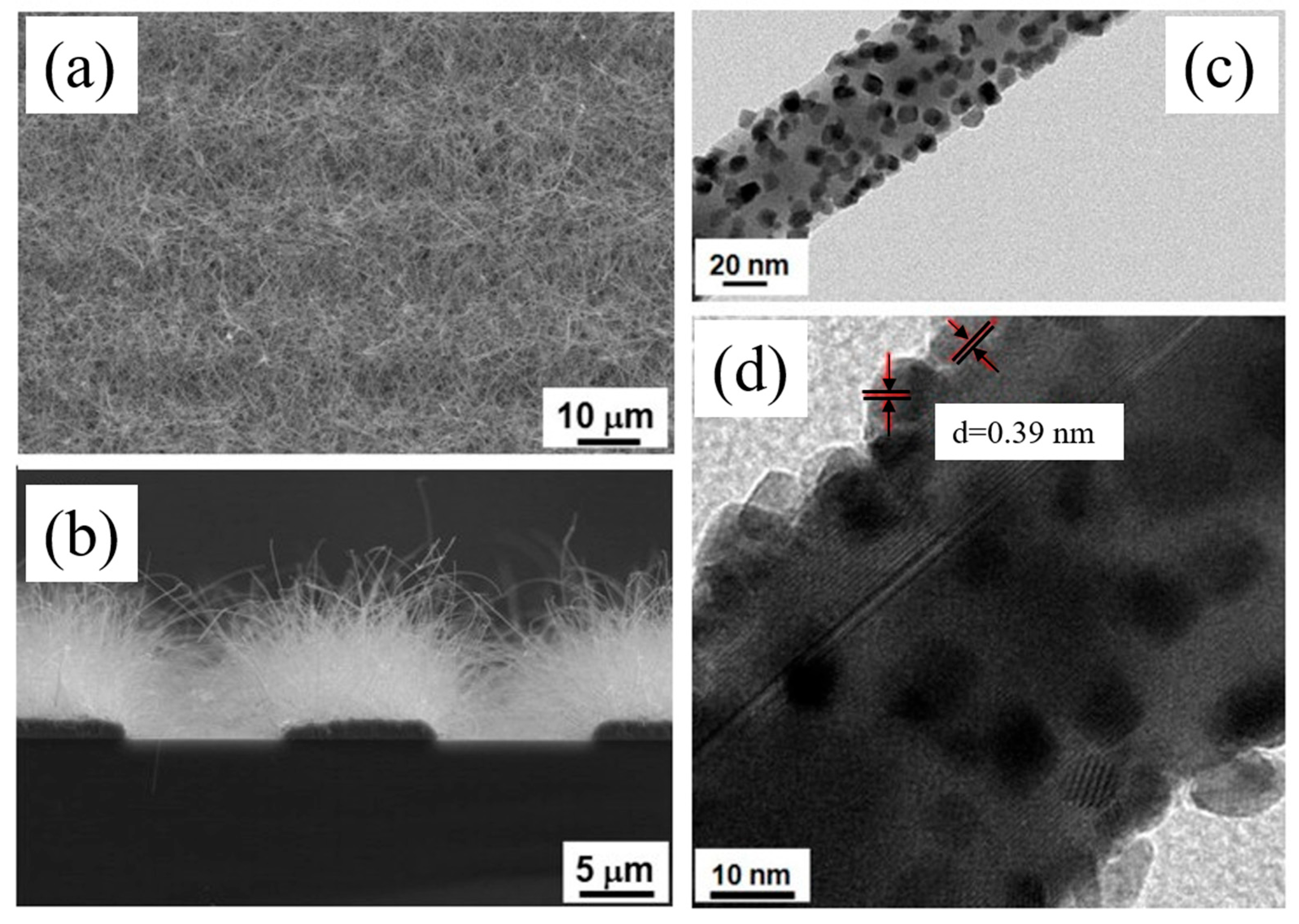
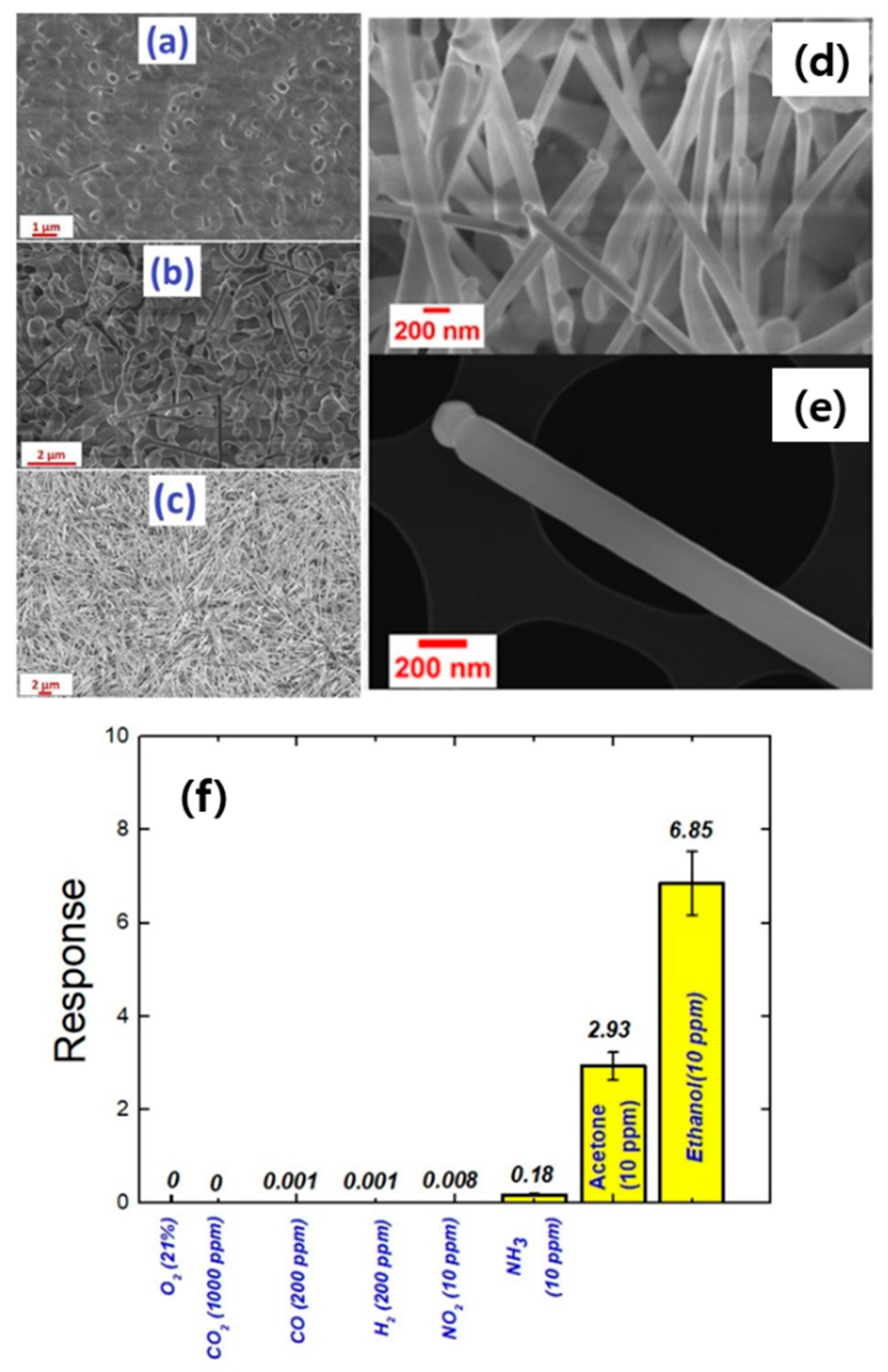
3.3. ZnO NWs
3.4. Other Metal Oxide NWs
4. Conclusions
Author Contributions
Funding
Institutional Review Board Statement
Informed Consent Statement
Data Availability Statement
Conflicts of Interest
References
- Abid, N.; Khan, A.M.; Shujait, S.; Chaudhary, K.; Ikram, M.; Imran, M.; Haider, J.; Khan, M.; Khan, Q.; Maqbool, M. Synthesis of nanomaterials using various top-down and bottom-up approaches, influencing factors, advantages. Adv. Colloid Interface Sci. 2022, 300, 102597. [Google Scholar] [CrossRef] [PubMed]
- Dick, K.A. A review of nanowire growth promoted by alloys and non-alloying elements with emphasis on Au-assisted III–V nanowires. Prog. Cryst. 2008, 54, 138–173. [Google Scholar] [CrossRef]
- Ramgir, N.S.; Yang, Y.; Zacharias, M. Nanowire-based sensors. Small 2010, 6, 1705–1722. [Google Scholar] [CrossRef] [PubMed]
- Murphy, C.J.; Jana, N.R. Controlling the aspect ratio of inorganic nanorods and nanowires. Adv. Mater. 2002, 14, 80–82. [Google Scholar] [CrossRef]
- Güniat, L.; Caroff, P.; Fontcuberta i Morral, A. Vapor phase growth of semiconductor nanowires: Key developments and open questions. Chem. Rev. 2019, 119, 8958–8971. [Google Scholar] [CrossRef] [PubMed]
- Pinion, C.W.; Christesen, J.D.; Cahoon, J.F. Understanding the vapor–liquid–solid mechanism of Si nanowire growth and doping to synthetically encode precise nanoscale morphology. J. Mater. Chem. C 2016, 4, 3890–3897. [Google Scholar] [CrossRef]
- Baig, N.; Kammakakam, I.; Falath, W. Nanomaterials: A review of synthesis methods, properties, recent progress, and challenges. Mater. Adv. 2021, 2, 1821–1871. [Google Scholar] [CrossRef]
- Hobbs, R.G.; Petkov, N.; Holmes, J.D. Semiconductor nanowire fabrication by bottom-up and top-down paradigms. Chem. Mater. 2012, 24, 1975–1991. [Google Scholar] [CrossRef]
- Biswas, A.; Bayer, I.S.; Biris, A.S.; Wang, T.; Dervishi, E.; Faupel, F. Advances in top-down and bottom–up surface nanofabrication: Techniques, applications & future prospects. Adv. Colloid Interface Sci. 2012, 170, 2–27. [Google Scholar]
- Obreja, P.; Cristea, D.; Dinescu, A.; Romaniţan, C. Influence of surface substrates on the properties of ZnO nanowires synthesized by hydrothermal method. Appl. Surf. Sci. 2019, 463, 1117–1123. [Google Scholar] [CrossRef]
- Ahn, S.E.; Ji, H.J.; Kim, K.; Kim, G.T.; Bae, C.H.; Park, S.M.; Kim, Y.K.; Ha, J.S. Origin of the slow photoresponse in an individual sol-gel synthesized ZnO nanowire. Appl. Phys. Lett. 2007, 90, 153106. [Google Scholar] [CrossRef]
- Khan, I.; Ibrahim, A.A.; Sohail, M.; Qurashi, A. Sonochemical assisted synthesis of RGO/ZnO nanowire arrays for photoelectrochemical water splitting. Ultrason. Sonochem. 2017, 37, 669–675. [Google Scholar] [CrossRef] [PubMed]
- Greyson, E.C.; Babayan, Y.; Odom, T.W. Directed growth of ordered arrays of small-diameter ZnO nanowires. Adv. Mater. 2004, 16, 1348–1352. [Google Scholar] [CrossRef]
- Youn, S.K.; Ramgir, N.; Wang, C.; Subannajui, K.; Cimalla, V.; Zacharias, M. Catalyst-free growth of ZnO nanowires based on topographical confinement and preferential chemisorption and their use for room temperature CO detection. J. Phys. Chem. 2010, 114, 10092–10100. [Google Scholar] [CrossRef]
- Liu, Z.; Zhang, D.; Han, S.; Li, C.; Tang, T.; Jin, W.; Liu, X.; Lei, B.; Zhou, C. Laser ablation synthesis and electron transport studies of tin oxide nanowires. Adv. Mater. 2003, 15, 1754–1757. [Google Scholar] [CrossRef]
- Piqueras, J.; Hidalgo, P. Growth of metal oxide nanostructures by thermal oxidation of metals under influence of external electric fields and electric current flow. Phys. Status Solidi (A) Appl. Mater. Sci. 2021, 218, 2100323. [Google Scholar] [CrossRef]
- Kim, H.W.; Kim, N.H. Synthesis of β-Ga2O3 nanowires by an MOCVD approach. Appl. Phys. A 2005, 81, 763–765. [Google Scholar] [CrossRef]
- Wagner, R.S.; Ellis, W.C. Vapor-liquid-solid mechanism of single crystal growth. Appl. Phys. Lett. 1964, 4, 89–90. [Google Scholar] [CrossRef]
- Redwing, J.M.; Miao, X.; Li, X. 9-Vapor-liquid-solid growth of semiconductor nanowires. In Handbook of Crystal Growth; Elsevier: Amsterdam, The Netherlands, 2015; pp. 399–439. [Google Scholar]
- Kodambaka, S.; Tersoff, J.; Reuter, M.C.; Ross, F.M. Diameter-independent kinetics in the vapor-liquid-solid growth of Si nanowires. Phys. Rev. Lett. 2006, 96, 096105. [Google Scholar] [CrossRef]
- Holonyak, N., Jr.; Wolfe, C.M.; Moore, J.S. Vapor-liquid-solid growth of gallium phosphide. Appl. Phys. Lett. 1965, 6, 64–65. [Google Scholar] [CrossRef]
- Givargizov, E.I. Fundamental aspects of VLS growth. J. Cryst. Growth 1975, 31, 20–30. [Google Scholar] [CrossRef]
- Wacaser, B.A.; Dick, K.A.; Johansson, J.; Borgström, M.T.; Deppert, K.; Samuelson, L. Preferential interface nucleation: An expansion of the VLS growth mechanism for nanowires. Adv. Mater. 2009, 21, 153–165. [Google Scholar] [CrossRef]
- Güell, F.; Martínez-Alanis, P.R. Tailoring the Green, Yellow and red defect emission bands in ZnO nanowires via the growth parameters. J. Lumin. 2019, 210, 128–134. [Google Scholar] [CrossRef]
- Kim, K.K.; Kim, D.; Kang, S.H.; Park, S. Detection of ethanol gas using In2O3 nanoparticle-decorated ZnS nanowires. Sens. Actuators B Chem. 2017, 248, 43–49. [Google Scholar] [CrossRef]
- McIntyre, P.C.; i Morral, A.F. Semiconductor nanowires: To grow or not to grow? Mater. Today Nano 2020, 9, 100058. [Google Scholar] [CrossRef]
- Shen, G.; Chen, P.C.; Ryu, K.; Zhou, C. Devices and chemical sensing applications of metal oxide nanowires. J. Mater. Chem. 2009, 19, 828–839. [Google Scholar] [CrossRef]
- Tiwale, N. Zinc oxide nanowire gas sensors: Fabrication, functionalisation and devices. Mater. Sci. Technol. 2015, 31, 1681–1697. [Google Scholar] [CrossRef]
- Bagga, S.; Akhtar, J.; Mishra, S. Synthesis and applications of ZnO nanowire: A review. AIP Conf. Proc. 2018, 1989, 020004. [Google Scholar]
- Galstyan, V.; Moumen, A.; Kumarage, G.W.; Comini, E. Progress towards chemical gas sensors: Nanowires and 2D semiconductors. Sens. Actuators B Chem. 2022, 357, 131466. [Google Scholar] [CrossRef]
- Comini, E. Metal oxides nanowires chemical/gas sensors: Recent advances. Mater. Today Adv. 2020, 7, 100099. [Google Scholar] [CrossRef]
- Fàbrega, C.; Casals, O.; Hernández-Ramírez, F.; Prades, J.D. A review on efficient self-heating in nanowire sensors: Prospects for very-low power devices. Sens. Actuators B Chem. 2018, 256, 797–811. [Google Scholar] [CrossRef]
- Mirzaei, A.; Lee, J.H.; Majhi, S.M.; Weber, M.; Bechelany, M.; Kim, H.W.; Kim, S.S. Resistive gas sensors based on metal-oxide nanowires. J. Appl. Phys. 2019, 126, 241102. [Google Scholar] [CrossRef]
- Wang, Y.; Duan, L.; Deng, Z.; Liao, J. Electrically transduced gas sensors based on semiconducting metal oxide nanowires. Sensors 2020, 20, 6781. [Google Scholar] [CrossRef] [PubMed]
- Zeng, H.; Zhang, G.; Nagashima, K.; Takahashi, T.; Hosomi, T.; Yanagida, T. Metal–oxide nanowire molecular sensors and their promises. Chemosensors 2021, 9, 41. [Google Scholar] [CrossRef]
- Mazouchi, M.; Poduri, S.; Dutta, M. Growth and characterization of indium oxide, zinc oxide and cadmium sulfide nanowires by vapor-liquid-solid growth technique. Appl. Phys. 2014, 6, 55. [Google Scholar] [CrossRef]
- Van Toan, N.; Van Tong, P.; Van Duy, N.; Hoa, N.D.; Van Hieu, N. Synthesis of single-crystal SnO2 nanowires for NOx gas sensors application. Ceram. Int. 2012, 38, 6557–6563. [Google Scholar]
- Lu, J.G.; Chang, P.; Fan, Z. Quasi-one-dimensional metal oxide materials-Synthesis, properties and applications. Mater. Sci. Eng. R Rep. 2006, 52, 49–91. [Google Scholar] [CrossRef]
- Wang, Z.L. Zinc oxide nanostructures: Growth, properties and applications. J. Phys. Condens. Matter 2004, 16, R829. [Google Scholar] [CrossRef]
- Fan, H.J.; Werner, P.; Zacharias, M. Semiconductor nanowires: From self-organization to patterned growth. Small 2006, 2, 700–717. [Google Scholar]
- Kolasinski, K.W. Catalytic growth of nanowires: Vapor–liquid–solid, vapor–solid–solid, solution–liquid–solid and solid–liquid–solid growth. Curr. Opin. Solid State Mater. Sci. 2006, 10, 182–191. [Google Scholar] [CrossRef]
- Oh, D.K.; Choi, H.; Shin, H.; Kim, K.; Kim, M.; Ok, J.G. Tailoring zinc oxide nanowire architectures collectively by catalytic vapor-liquid-solid growth, catalyst-free vapor-solid growth, and low-temperature hydrothermal growth. Ceram. Int. 2021, 47, 2131–2143. [Google Scholar] [CrossRef]
- Comini, E.; Baratto, C.; Faglia, G.; Ferroni, M.; Vomiero, A.; Sberveglieri, G. Quasi-one dimensional metal oxide semiconductors: Preparation, characterization and application as chemical sensors. Prog. Mater. Sci. 2009, 54, 1–67. [Google Scholar] [CrossRef]
- Wu, Y.; Yan, H.; Huang, M.; Messer, B.; Song, J.H.; Yang, P. Inorganic semiconductor nanowires: Rational growth, assembly, and novel properties. Chem. Eur. J. 2002, 8, 1260–1268. [Google Scholar] [CrossRef] [PubMed]
- Kim, H.W.; Shim, S.H. Growth of MgO nanowires assisted by the annealing treatment of Au-coated substrates. Chem. Phys. Lett. 2006, 422, 165–169. [Google Scholar] [CrossRef]
- Choi, H.J. Vapor–liquid–solid growth of semiconductor nanowires. In Semiconductor Nanostructures for Optoelectronic Devices: Processing, Characterization and Applications; Springer: Berlin/Heidelberg, Germany, 2011; pp. 1–36. [Google Scholar]
- O’Regan, C.; Biswas, S.; Petkov, N.; Holmes, J.D. Recent advances in the growth of germanium nanowires: Synthesis, growth dynamics and morphology control. J. Mater. Chem. C 2014, 2, 14–33. [Google Scholar] [CrossRef]
- Sutter, E.; Sutter, P. Ultrathin twisted germanium sulfide van der Waals nanowires by bismuth catalyzed vapor–liquid–solid growth. Small 2021, 17, 2104784. [Google Scholar] [CrossRef] [PubMed]
- Dalal, S.H.; Baptista, D.L.; Teo, K.B.K.; Lacerda, R.G.; Jefferson, D.A.; Milne, W.I. Controllable growth of vertically aligned zinc oxide nanowires using vapour deposition. Nanotechnology 2006, 17, 4811. [Google Scholar] [CrossRef]
- Akbari, M.; Mohajerzadeh, S. Highly patterned growth of SnO2 nanowires using a sub-atmospheric vapor–liquid–solid deposition. J. Phys. D Appl. Phys. 2017, 50, 305104. [Google Scholar] [CrossRef]
- Chen, Y.; Cui, X.; Zhang, K.; Pan, D.; Zhang, S.; Wang, B.; Hou, J.G. Bulk-quantity synthesis and self-catalytic VLS growth of SnO2 nanowires by lower-temperature evaporation. Chem. Phys. Lett. 2003, 369, 16–20. [Google Scholar] [CrossRef]
- Araújo, E.P.D.; Paiva, M.P.; Moisés, L.A.; Santo, G.S.D.E.; Blanco, K.C.; Chiquito, A.J.; Amorim, C.A. Improving hazardous gas detection behavior with palladium decorated SnO2 nanobelts networks. Sensors 2023, 23, 4783. [Google Scholar] [CrossRef]
- Gutsche, C.; Regolin, I.; Blekker, K.; Lysov, A.; Prost, W.; Tegude, F.J. Controllable p-type doping of GaAs nanowires during vapor-liquid-solid growth. J. Appl. Phys. 2009, 105, 024305. [Google Scholar] [CrossRef]
- Costa, I.M.; Colmenares, Y.N.; Pizani, P.S.; Leite, E.R.; Chiquito, A.J. Sb doping of VLS synthesized SnO2 nanowires probed by Raman and XPS spectroscopy. Chem. Phys. Lett. 2018, 695, 125–130. [Google Scholar] [CrossRef]
- El-Maghraby, E.M.; Qurashi, A.; Yamazaki, T. Synthesis of SnO2 nanowires their structural and H2 gas sensing properties. Ceram. Int. 2013, 39, 8475–8480. [Google Scholar] [CrossRef]
- Kim, H.W.; Shim, S.H.; Lee, J.W.; Park, J.Y.; Kim, S.S. Bi2Sn2O7 nanoparticles attached to SnO2 nanowires and used as catalysts. Chem. Phys. Lett. 2008, 456, 193–197. [Google Scholar] [CrossRef]
- Kar, A.; Yang, J.; Dutta, M.; Stroscio, M.A.; Kumari, J.; Meyyappan, M. Rapid thermal annealing effects on tin oxide nanowires prepared by vapor–liquid–solid technique. Nanotechnology 2009, 20, 065704. [Google Scholar] [CrossRef] [PubMed]
- Calestani, D.; Zha, M.; Salviati, G.; Lazzarini, L.; Zanotti, L.; Comini, E.; Sberveglieri, G. Nucleation and growth of SnO2 nanowires. J. Cryst. Growth. 2005, 275, e2083–e2087. [Google Scholar] [CrossRef]
- Thong, L.V.; Loan, L.T.N.; Van Hieu, N. Comparative study of gas sensor performance of SnO2 nanowires and their hierarchical nanostructures. Sens. Actuators B Chem. 2010, 150, 112–119. [Google Scholar] [CrossRef]
- Jung, S.H.; Choi, S.W.; Kim, S.S. Fabrication and properties of trench-structured networked SnO2 nanowire gas sensors. Sens. Actuators B Chem. 2012, 171, 672–678. [Google Scholar] [CrossRef]
- Her, Y.C.; Chiang, C.K.; Jean, S.T.; Huang, S.L. Self-catalytic growth of hierarchical In2O3 nanostructures on SnO2 nanowires and their CO sensing properties. CrystEngComm 2012, 14, 1296–1300. [Google Scholar] [CrossRef]
- Park, J.H.; Cho, M.S.; Lim, D.; Park, J.G. SnO2 nanowire gas sensor operating at room temperature. J. Nanosci. Nanotechnol. 2014, 14, 8038–8042. [Google Scholar] [CrossRef]
- Choi, Y.J.; Hwang, I.S.; Park, J.G.; Choi, K.J.; Park, J.H.; Lee, J.H. Novel fabrication of an SnO2 nanowire gas sensor with high sensitivity. Nanotechnology 2008, 19, 095508. [Google Scholar] [CrossRef] [PubMed]
- Wei, D.; Shen, Y.; Li, M.; Liu, W.; Gao, S.; Jia, L.; Cui, B. Synthesis and characterization of single-crystalline SnO2 nanowires. J. Nanomater. 2013, 2013, 20. [Google Scholar] [CrossRef]
- Kim, H.; Cai, Z.; Chang, S.P.; Park, S. Improved sub-ppm acetone sensing properties of SnO2 nanowire-based sensor by attachment of Co3O4 nanoparticles. J. Mater. Res. Technol. 2020, 9, 1129–1136. [Google Scholar] [CrossRef]
- Choi, K.S.; Park, S.; Chang, S.P. Enhanced ethanol sensing properties based on SnO2 nanowires coated with Fe2O3 nanoparticles. Sens. Actuators B Chem. 2017, 238, 871–879. [Google Scholar] [CrossRef]
- Navale, S.; Shahbaz, M.; Majhi, S.M.; Mirzaei, A.; Kim, H.W.; Kim, S.S. CuxO nanostructure-based gas sensors for H2S detection: An overview. Chemosensors 2021, 9, 127. [Google Scholar] [CrossRef]
- Kim, S.S.; Na, H.G.; Choi, S.W.; Kwak, D.S.; Kim, H.W. Novel growth of CuO-functionalized, branched SnO2 nanowires and their application to H2S sensors. J. Phys. D Appl. Phys. 2012, 45, 205301. [Google Scholar] [CrossRef]
- Bang, J.H.; Choi, M.S.; Mirzaei, A.; Oum, W.; Han, S.; Kim, S.S.; Kim, H.W. Porous Si/SnO2 nanowires heterostructures for H2S gas sensing. Ceram. Int. 2020, 46, 604–611. [Google Scholar] [CrossRef]
- Choi, S.W.; Jung, S.H.; Kim, S.S. Functionalization of selectively grown networked SnO2 nanowires with Pd nanodots by γ-ray radiolysis. Nanotechnology 2011, 22, 225501. [Google Scholar] [CrossRef]
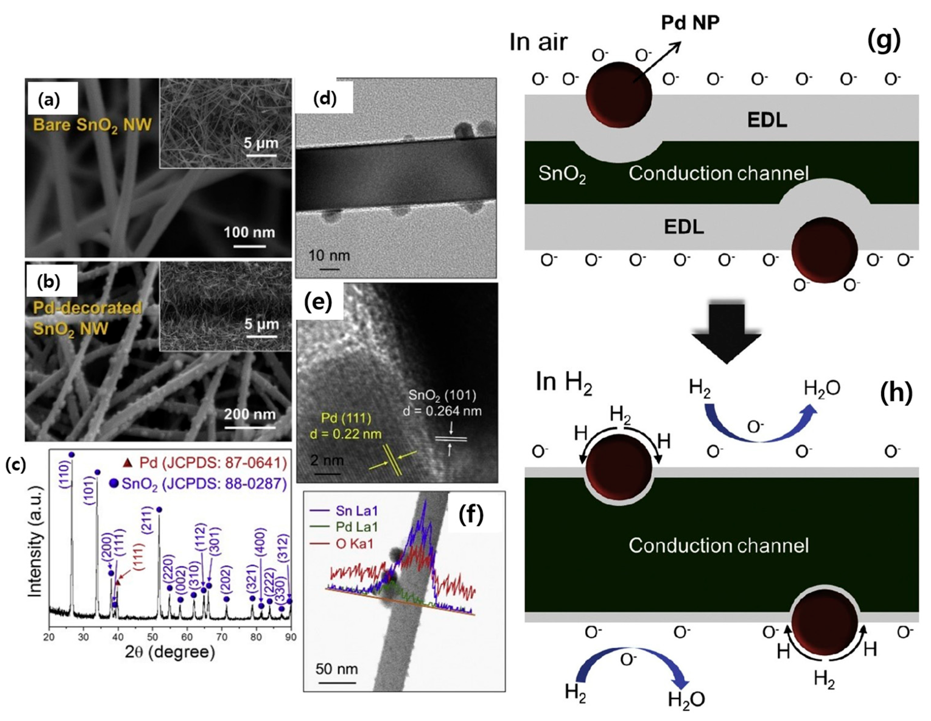
- Kim, J.H.; Mirzaei, A.; Kim, H.W.; Kim, S.S. Improving the hydrogen sensing properties of SnO2 nanowire-based conductometric sensors by Pd-decoration. Sens. Actuators B Chem. 2019, 285, 358–367. [Google Scholar] [CrossRef]
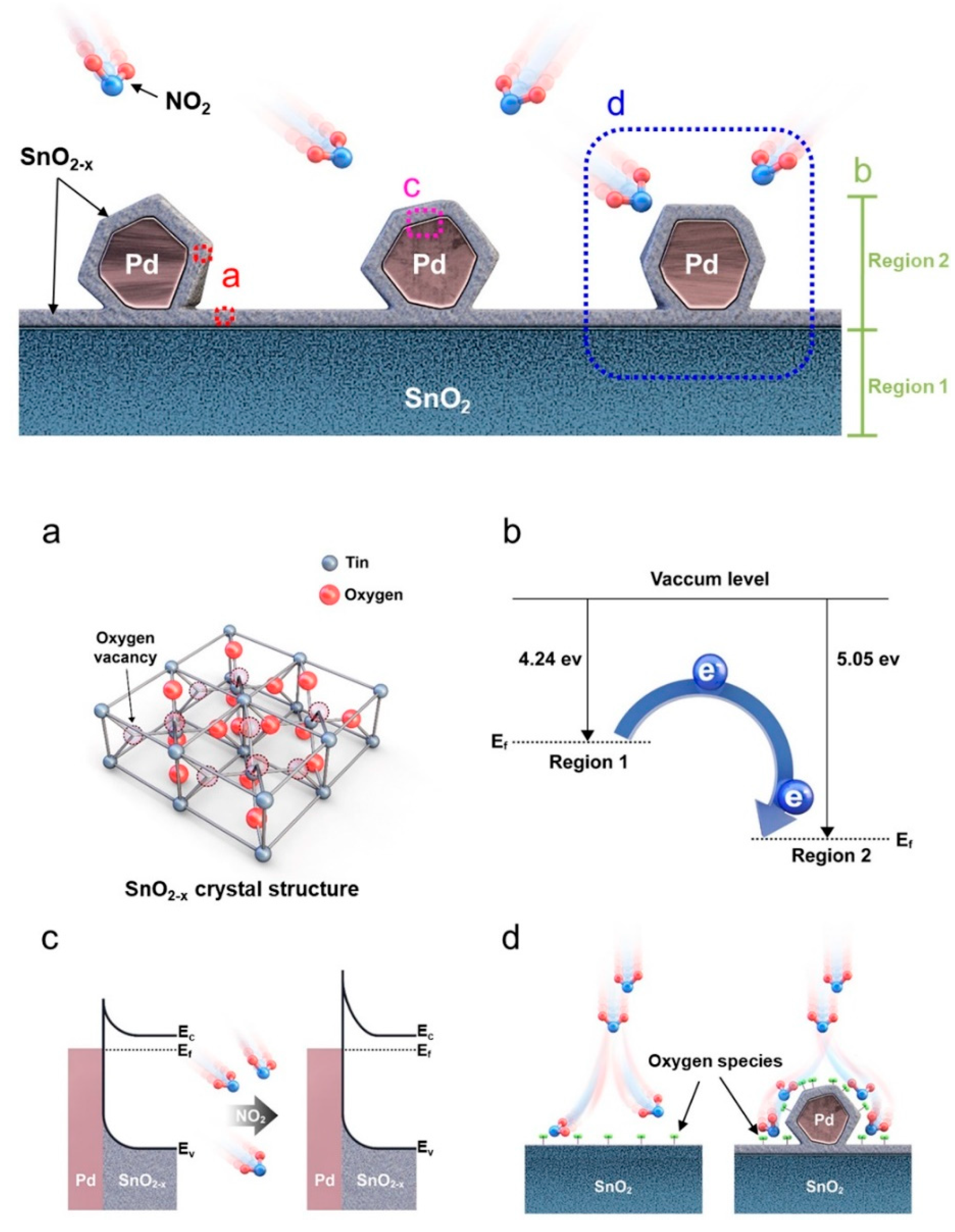
- Choi, M.S.; Mirzaei, A.; Na, H.G.; Kim, S.; Kim, D.E.; Lee, K.H.; Choi, S.W. Facile and fast decoration of SnO2 nanowires with Pd embedded SnO2-x nanoparticles for selective NO2 gas sensing. Sens. Actuators B Chem. 2021, 340, 129984. [Google Scholar] [CrossRef]
- Zeng, F.; Zhang, X.; Wang, J.; Wang, L.; Zhang, L. Large-scale growth of In2O3 nanowires and their optical properties. Nanotechnology 2004, 15, 596. [Google Scholar] [CrossRef]
- Guo, D.L.; Huang, X.; Xing, G.Z.; Zhang, Z.; Li, G.P.; He, M.; Wu, T. Metal-layer-assisted coalescence of Au nanoparticles and its effect on diameter control in vapor-liquid-solid growth of oxide nanowires. Phys. Rev. B 2011, 83, 045403. [Google Scholar] [CrossRef]
- Kuo, C.H.; Chang, P.Y.; Chen, W.H.; Lin, S.J. Synthesis of transparent metallic Sn-doped In2O3 nanowires: Effects of doping concentration on photoelectric properties. Phys. Status Solidi Appl. Mater. Sci. 2014, 211, 488–493. [Google Scholar] [CrossRef]
- Tuzluca, F.N.; Yesilbag, Y.O.; Akkus, T.; Ertugrul, M. Effects of graphite on the synthesis of 1-D single crystal In2O3 nanostructures at high temperature. Mater. Sci. Semicond. 2017, 66, 62–68. [Google Scholar] [CrossRef]
- Ramos Ramon, J.A.; Cremades, A.; Maestre, D.; Silva Gonzalez, R.; Pal, U. Fabricating necklace-, tower-, and rod-shaped In2O3 nanostructures by controlling saturation kinetics of catalyst droplets in a vapor–liquid–solid process. Cryst. Growth Des. 2017, 17, 4596–4602. [Google Scholar] [CrossRef]
- Tuzluca, F.N.; Yesilbag, Y.O.; Ertugrul, M. Synthesis of In2O3 nanostructures with different morphologies as potential supercapacitor electrode materials. Appl. Surf. Sci. 2018, 427, 956–964. [Google Scholar] [CrossRef]
- Singh, N.; Zhang, T.; Lee, P.S. The temperature-controlled growth of In2O3 nanowires, nanotowers and ultra-long layered nanorods. Nanotechnology 2009, 20, 195605. [Google Scholar] [CrossRef]
- Hadia, N.M.A.; Mohamed, H.A. Synthesis, structure and optical properties of single-crystalline In2O3 nanowires. J. Alloys Compd. 2013, 547, 63–67. [Google Scholar] [CrossRef]
- Vomiero, A.; Bianchi, S.; Comini, E.; Faglia, G.; Ferroni, M.; Poli, N.; Sberveglieri, G. In2O3 nanowires for gas sensors: Morphology and sensing characterisation. Thin Solid Film. 2007, 515, 8356–8359. [Google Scholar] [CrossRef]
- Moon, S.E.; Kim, E.K.; Lee, H.Y.; Lee, J.W.; Park, S.J.; Kwak, J.H.; Lee, T.H. Fabrication and NO2 sensing characteristics of an In2O3 nanowire gas sensor. J. Korean Phys. Soc. 2009, 54, 830–834. [Google Scholar] [CrossRef]
- Son, D.N.; Hung, C.M.; Le, D.T.T.; Xuan, C.T.; Van Duy, N.; Dich, N.Q.; Hoa, N.D. A novel design and fabrication of self-heated In2O3 nanowire gas sensor on glass for ethanol detection. Sens. Actuators A Phys. 2022, 345, 113769. [Google Scholar] [CrossRef]
- Qurashi, A.; El-Maghraby, E.M.; Yamazaki, T.; Shen, Y.; Kikuta, T. A generic approach for controlled synthesis of In2O3 nanostructures for gas sensing applications. J. Alloys Compd. 2009, 481, L35–L39. [Google Scholar] [CrossRef]
- Wang, X.; Zhang, W.; Wang, X.; Li, X.; Sui, X.; Liu, G.; Zhang, Z. Facile fabrication of NiO foam@ Sn-doped In2O3 nanowire heterosturctures for highly sensitive ethylene glycol gas sensors at low temperatures. Sens. Actuators B Chem. 2023, 377, 132991. [Google Scholar] [CrossRef]
- Singh, N.; Ponzoni, A.; Comini, E.; Lee, P.S. Chemical sensing investigations on Zn–In2O3 nanowires. Sens. Actuators B Chem. 2012, 171, 244–248. [Google Scholar] [CrossRef]
- Vomiero, A.; Bianchi, S.; Comini, E.; Faglia, G.; Ferroni, M.; Sberveglieri, G. Controlled growth and sensing properties of In2O3 nanowires. Cryst. Growth Des. 2007, 7, 2500–2504. [Google Scholar] [CrossRef]
- Qurashi, A.; El-Maghraby, E.M.; Yamazaki, T.; Kikuta, T. Catalyst supported growth of In2O3 nanostructures and their hydrogen gas sensing properties. Sens. Actuators B Chem. 2010, 147, 48–54. [Google Scholar] [CrossRef]
- Kim, S.S.; Park, J.Y.; Choi, S.W.; Kim, H.S.; Na, H.G.; Yang, J.C.; Kim, H.W. Significant enhancement of the sensing characteristics of In2O3 nanowires by functionalization with Pt nanoparticles. Nanotechnology 2010, 21, 415502. [Google Scholar] [CrossRef]
- Park, S. Acetone gas detection using TiO2 nanoparticles functionalized In2O3 nanowires for diagnosis of diabetes. J. Alloys Compd. 2017, 696, 655–662. [Google Scholar] [CrossRef]
- Kim, S.S.; Park, J.Y.; Choi, S.W.; Na, H.G.; Yang, J.C.; Kim, H.W. Enhanced NO2 sensing characteristics of Pd-functionalized networked In2O3 nanowires. J. Alloys Compd. 2011, 509, 9171–9177. [Google Scholar] [CrossRef]
- Wang, S.H.; Chang, S.J.; Liu, S.; Tsai, T.Y.; Hsu, C.L. Synthesis of In2O3 nanowires and their gas sensing properties. IEEE Sens. J. 2016, 16, 5850–5855. [Google Scholar] [CrossRef]
- Lee, J.; Lee, S.H.; Bak, S.Y.; Kim, Y.; Woo, K.; Lee, S.; Yi, M. Improved sensitivity of α-Fe2O3 nanoparticle-decorated ZnO nanowire gas sensor for CO. Sensors 2019, 19, 1903. [Google Scholar] [CrossRef]
- Kim, S.S.; Choi, S.W.; Na, H.G.; Kwak, D.S.; Kwon, Y.J.; Kim, H.W. ZnO–SnO2 branch–stem nanowires based on a two-step process: Synthesis and sensing capability. Curr. Appl. Phys. 2013, 13, 526–532. [Google Scholar] [CrossRef]
- Kim, H.W.; Kebede, M.A.; Kim, H.S.; Srinivasa, B.; Kim, D.Y.; Park, J.Y.; Kim, S.S. Effect of growth temperature on the ZnO nanowires prepared by thermal heating of Zn powders. Curr. Appl. Phys. 2010, 10, 52–56. [Google Scholar] [CrossRef]
- Kim, J.H.; Lee, J.H.; Park, Y.; Kim, J.Y.; Mirzaei, A.; Kim, H.W.; Kim, S.S. Toluene-and benzene-selective gas sensors based on Pt-and Pd-functionalized ZnO nanowires in self-heating mode. Sens. Actuators B Chem. 2019, 294, 78–88. [Google Scholar] [CrossRef]
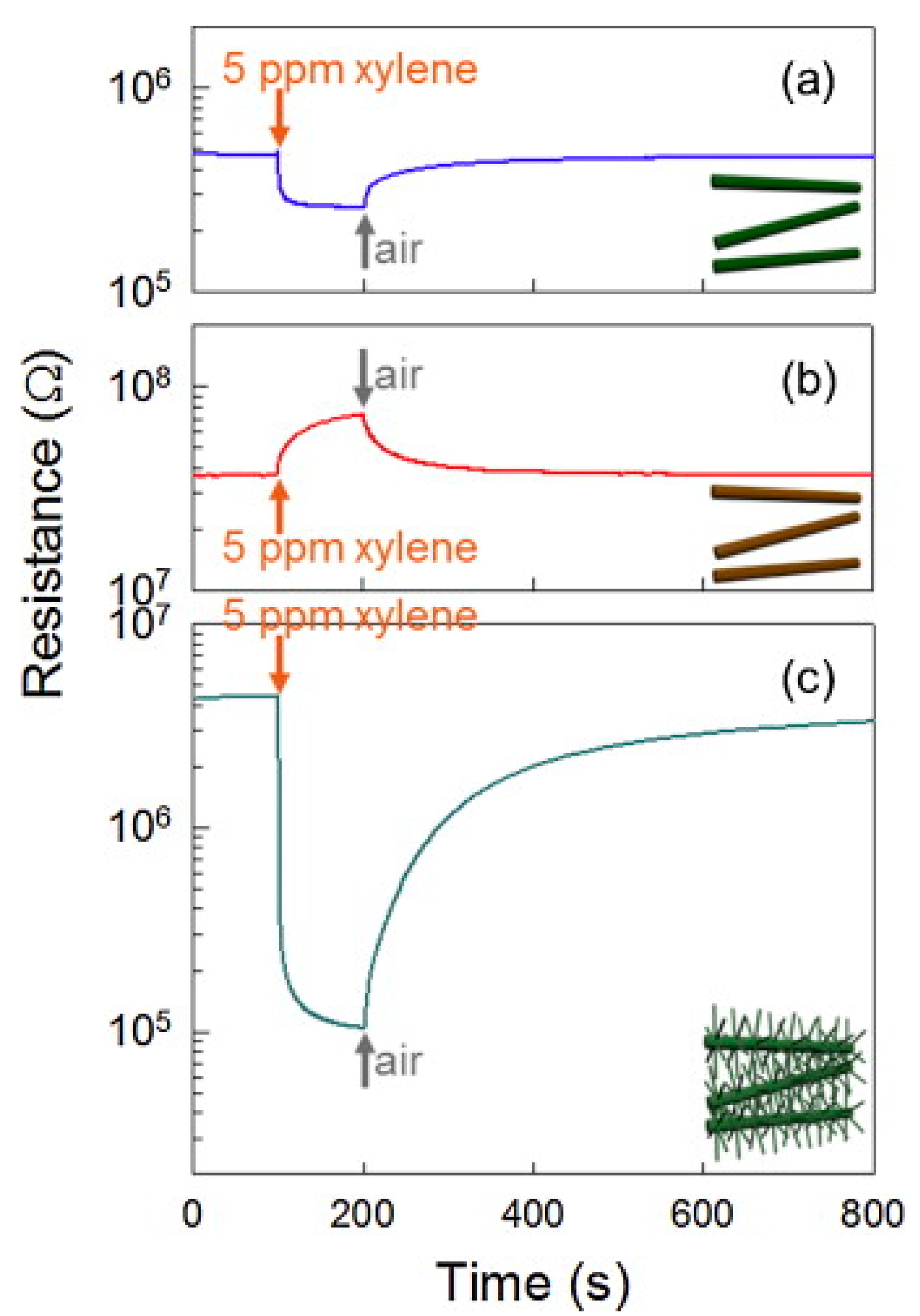
- Woo, H.S.; Kwak, C.H.; Chung, J.H.; Lee, J.H. Highly selective and sensitive xylene sensors using Ni-doped branched ZnO nanowire networks. Sens. Actuators B Chem. 2015, 216, 358–366. [Google Scholar] [CrossRef]
- Woo, H.S.; Kwak, C.H.; Chung, J.H.; Lee, J.H. Co-doped branched ZnO nanowires for ultraselective and sensitive detection of xylene. ACS Appl. Mater. Interfaces 2014, 6, 22553–22560. [Google Scholar] [CrossRef] [PubMed]
- Choi, S.W.; Kim, S.S. Room temperature CO sensing of selectively grown networked ZnO nanowires by Pd nanodot functionalization. Sens. Actuators B Chem. 2012, 168, 8–13. [Google Scholar] [CrossRef]
- Kim, J.H.; Mirzaei, A.; Kim, H.W.; Kim, S.S. Low-voltage-driven sensors based on ZnO nanowires for room-temperature detection of NO2 and CO gases. ACS Appl. Mater. Interfaces 2019, 11, 24172–24183. [Google Scholar] [CrossRef]
- Park, J.Y.; Choi, S.W.; Kim, S.S. Tailoring the number of junctions per electrode pair in networked ZnO nanowire sensors. J. Am. Ceram. Soc. 2011, 94, 3922–3926. [Google Scholar] [CrossRef]
- Singh, M.; Kaur, N.; Comini, E. The role of self-assembled monolayers in electronic devices. J. Mater. Chem. C 2020, 8, 3938–3955. [Google Scholar] [CrossRef]
- Singh, M.; Kaur, N.; Drera, G.; Casotto, A.; Sangaletti, L.; Comini, E. SAM functionalized ZnO nanowires for selective acetone detection: Optimized surface specific interaction using APTMS and GLYMO monolayers. Adv. Funct. Mater. 2020, 30, 2003217. [Google Scholar] [CrossRef]
- Moumen, A.; Zappa, D.; Poli, N.; Comini, E. Catalyst–Assisted vapor liquid solid growth of α-Bi2O3 nanowires for acetone and ethanol detection. Sens. Actuators B Chem. 2021, 346, 130432. [Google Scholar] [CrossRef]
- Kaur, N.; Zappa, D.; Poli, N.; Comini, E. Integration of VLS-Grown WO3 Nanowires into Sensing Devices for the Detection of H2S and O3. ACS Omega 2019, 4, 16336–16343. [Google Scholar] [CrossRef] [PubMed]
- Kaur, N.; Comini, E.; Poli, N.; Zappa, D.; Sberveglieri, G. Nickel oxide nanowires growth by VLS technique for gas sensing application. Procedia Eng. 2015, 120, 760–763. [Google Scholar] [CrossRef]
- Kaur, N.; Comini, E.; Zappa, D.; Poli, N.; Sberveglieri, G. Nickel oxide nanowires: Vapor liquid solid synthesis and integration into a gas sensing device. Nanotechnology 2016, 27, 205701. [Google Scholar] [CrossRef] [PubMed]
- Kaur, N.; Zappa, D.; Ferroni, M.; Poli, N.; Campanini, M.; Negrea, R.; Comini, E. Branch-like NiO/ZnO heterostructures for VOC sensing. Sens. Actuators B Chem. 2018, 262, 477–485. [Google Scholar] [CrossRef]
- Kim, H.W.; Kim, N.H. Growth of β-Ga2O3 nanobelts on Ir-coated substrates. Appl. Phys. A 2005, 80, 537–540. [Google Scholar] [CrossRef]
- Weng, T.F.; Ho, M.S.; Sivakumar, C.; Balraj, B.; Chung, P.F. VLS growth of pure and Au decorated β-Ga2O3 nanowires for room temperature CO gas sensor and resistive memory applications. Appl. Surf. Sci. 2020, 533, 147476. [Google Scholar] [CrossRef]
- Lukowski, M.A.; Jin, S. Improved synthesis and electrical properties of Si-doped α-Fe2O3 nanowires. J. Phys. Chem. C 2011, 115, 12388–12395. [Google Scholar] [CrossRef]
- Srivastava, H.; Tiwari, P.; Srivastava, A.K.; Nandedkar, R.V. Growth and characterization of α-Fe2O3 nanowires. J. Appl. Phys. 2007, 102, 054303. [Google Scholar] [CrossRef]
- Wen, X.; Wang, S.; Ding, Y.; Wang, Z.L.; Yang, S. Controlled growth of large-area, uniform, vertically aligned arrays of α-Fe2O3 nanobelts and nanowires. J. Phys. Chem. B 2005, 109, 215–220. [Google Scholar] [CrossRef]
- Tian, W.; Wang, X.; Zhi, C.; Zhai, T.; Liu, D.; Zhang, C.; Bando, Y. Ni(OH)2 nanosheet@ Fe2O3 nanowire hybrid composite arrays for high-performance supercapacitor electrodes. Nano Energy 2013, 2, 754–763. [Google Scholar] [CrossRef]
- Morber, J.R.; Ding, Y.; Haluska, M.S.; Li, Y.; Liu, J.P.; Wang, Z.L.; Snyder, R.L. PLD-assisted VLS growth of aligned ferrite nanorods, nanowires, and nanobelts synthesis, and properties. J. Phys. Chem. B 2006, 110, 21672–21679. [Google Scholar] [CrossRef]
- Majhi, S.M.; Mirzaei, A.; Kim, H.W.; Kim, S.S. Reduced graphene oxide (rGO)-loaded metal-oxide nanofiber gas sensors: An overview. Sensors 2021, 21, 1352. [Google Scholar] [CrossRef]
- Kwon, Y.J.; Kang, S.Y.; Mirzaei, A.; Choi, M.S.; Bang, J.H.; Kim, S.S.; Kim, H.W. Enhancement of gas sensing properties by the functionalization of ZnO-branched SnO2 nanowires with Cr2O3 nanoparticles. Sens. Actuators B Chem. 2017, 249, 656–666. [Google Scholar] [CrossRef]
- Ramgir, N.; Datta, N.; Kaur, M.; Kailasaganapathi, S.; Debnath, A.K.; Aswal, D.K.; Gupta, S. K Metal oxide nanowires for chemiresistive gas sensors: Issues, challenges and prospects. Colloids Surf. A Physicochem. Eng. Asp. 2013, 439, 101–116. [Google Scholar] [CrossRef]


| Sensing Material | Gas | Conc. (ppm) | T (°C) | Response (Ra/Rg) or (Rg/Ra) | LOD (ppm) | tres(s)/trec(s) | Selectivity Ratio | Ref. |
|---|---|---|---|---|---|---|---|---|
| SnO2 NWs | H2 | 1000 | 100 | 12 (ΔR/Rg) | 100 | ~180/~180 | - | [55] |
| SnO2 NWs | O2 | 1 torr | RT | 30% [(ΔR/Rg) × 100] | 0.05 torr | ~200/~250 | - | [56] |
| SnO2 hierarchical NWs | LPG | 2000 | 350 | 20 | 500 | ~4/~8 | - | [59] |
| SnO2 hierarchical NWs | NH3 | 300 | 200 | 10.9 | 300 | ~16/~25 | - | [59] |
| SnO2 NWs | NO2 | 100 | 300 | 25 | 5 | ~600/~700 | - | [60] |
| In2O3 NWs | CO | 10 | 300 | 1.4 | 10 | ~240/~460 | - | [61] |
| SnO2 NWs | NO2 | 10 | 200 | 43% | 1 | ~38/~25 | - | [62] |
| SnO2 NWs | NO2 | 0.5 | 200 | 20 | 0.5 | 43/18 | - | [63] |
| SnO2 NWs | H2 | 1000 | 150 | 6 (ΔR/Rg) | 100 | -/- | - | [64] |
| Co3O4-decorated SnO2 NWs | C6H3O | 50 | 300 | 63 | 0.5 | 10/~300 | 2.2 | [65] |
| Fe2O3-decorated SnO2 NWs | C2H5OH | 200 | 300 | 60 | 0.5 | ~60/~110 | 1.58 | [66] |
| CuO-decorated SnO2 NWs | H2S | 1 | 300 | 5 | 1 | ~300/~400 | - | [68] |
| Porous Si/SnO2 NWs | H2S | 20 | 100 | 2 | 10 | ~200/~230 | 1.8 | [69] |
| Pd-decorated SnO2 NWs | NO2 | 30 | 300 | 1.56 | 0.1 | ~470/~460 | - | [70] |
| Pd-decorated SnO2 NWs | H2 | 1 | 300 | 8 | 0.1 | ~250/~300 | 8 | [71] |
| Pd-decorated SnO2 NWs | NO2 | 2 | 25 | 6 | 2 | ~380/~1000 | 9.8 | [72] |
| In2O3 NWs | C3H6O | 500 | Heat@ 1.06 mW | 1.3 | 10 | 10/50 | 1.2 | [83] |
| NiO foam@Sn-doped In2O3 NWs | Ethylene glycol | 100 | 125 | 170 | 1 | ~9/~20 | 16 | [85] |
| ZnO-doped In2O3 NWs | C2H5OH | 100 | 200 | 62 | - | -/- | 2 | [86] |
| In2O3 NWs | H2 | 500 | 200 | 0.7 (ΔR/Rg) | 500 | 31/80 | - | [88] |
| Pt-decorated In2O3 NWs | O2 | 400 | 50 | 1.5 | 10 | ~70/~500 | - | [89] |
| TiO2 decorated In2O3 NWs | C2H5OH | 10 | 250 | 34 | 0.10 | ~15/~130 | ~2 | [90] |
| Pd-decorated In2O3 NWs | NO2 | 3 | 50 | 3.5 (ΔR/Rg) | 3 | 60/365 | - | [91] |
| Fe2O3-decorated ZnO NWs | CO | 100 | 300 | 19 | 1 | ~100/~100 | 3 | [93] |
| ZnO-branched SnO2 NWs | NO2 | 100 | 250 | 6 | 0.5 | ~1000/~12,000 | - | [94] |
| Ni-doped branched ZnO NWs | Xylene | 5 | 400 | 42 | 0.25 | ~80/~400 | 1.9 | [97] |
| Pd-decorated ZnO NWs | CO | 0.1 | 25 | 1.02 | 0.1 | 210/400 | - | [99] |
Disclaimer/Publisher’s Note: The statements, opinions and data contained in all publications are solely those of the individual author(s) and contributor(s) and not of MDPI and/or the editor(s). MDPI and/or the editor(s) disclaim responsibility for any injury to people or property resulting from any ideas, methods, instructions or products referred to in the content. |
© 2023 by the authors. Licensee MDPI, Basel, Switzerland. This article is an open access article distributed under the terms and conditions of the Creative Commons Attribution (CC BY) license (https://creativecommons.org/licenses/by/4.0/).
Share and Cite
Mirzaei, A.; Lee, M.H.; Pawar, K.K.; Bharath, S.P.; Kim, T.-U.; Kim, J.-Y.; Kim, S.S.; Kim, H.W. Metal Oxide Nanowires Grown by a Vapor–Liquid–Solid Growth Mechanism for Resistive Gas-Sensing Applications: An Overview. Materials 2023, 16, 6233. https://doi.org/10.3390/ma16186233
Mirzaei A, Lee MH, Pawar KK, Bharath SP, Kim T-U, Kim J-Y, Kim SS, Kim HW. Metal Oxide Nanowires Grown by a Vapor–Liquid–Solid Growth Mechanism for Resistive Gas-Sensing Applications: An Overview. Materials. 2023; 16(18):6233. https://doi.org/10.3390/ma16186233
Chicago/Turabian StyleMirzaei, Ali, Myoung Hoon Lee, Krishna K. Pawar, Somalapura Prakasha Bharath, Tae-Un Kim, Jin-Young Kim, Sang Sub Kim, and Hyoun Woo Kim. 2023. "Metal Oxide Nanowires Grown by a Vapor–Liquid–Solid Growth Mechanism for Resistive Gas-Sensing Applications: An Overview" Materials 16, no. 18: 6233. https://doi.org/10.3390/ma16186233