Abstract
atomic thin monolayer () was synthesized recently. Interest in the is based on its close relation to layers in typical high temperature cuprate superconductors. Here, we present the calculation of the band structure, the density of states and the Fermi surface of the flat as well as the corrugated within the density functional theory (DFT) in the generalized gradient approximation (GGA). In the flat , the - band crosses the Fermi level, while the - hybridized band is located just below it. The corrugation leads to a significant shift of the - hybridized band down in energy and a degeneracy lifting for the - bands. Corrugated is more energetically favorable than the flat one. In addition, we compared the electronic structure of the considered monolayers with bulk systems. We also investigated the influence of a crystal lattice strain (which might occur on some interfaces) on the electronic structure of both and determined the critical strains of topological Lifshitz transitions. Finally, we proposed a number of different minimal models for the flat and the corrugated using projections onto different Wannier functions basis sets and obtained the corresponding Hamiltonian matrix elements in a real space.
1. Introduction
Copper oxides stand apart from other transition metal compounds. First of all, they attract much attention because of their high temperature superconductivity (HTSC) and already existing applications [1,2,3,4,5] as catalysts [6], photocells [7] and thin-film transistors [8]. is an exceptional member of the generally rocksalt family ( to ), as it deviates both structurally and electronically from others. Unlike other members of the transition oxides, which crystallize in the cubic rocksalt structure (with possible rhombohedral distortions), Tenorite (CuO) crystallizes in the lower symmetry monoclinic (C2/c) crystal structure [9], albeit the cubic crystal structure is also possible [10]. Thus far, the bulk compound has been thoroughly studied using ab initio calculations: DFT+U [11,12,13,14,15], DFT with hybrid functional [4] and Charge Transition Level Approach [16].
The relatively recent interest in the monolayer arose in part because one would expect a superconducting phase to occur here by analogy with the typical representative of HTSC cuprates . There, the superconductivity occurs in two-dimensional layers formed by plaquettes. The monolayer consists of the same plaquettes. However, the plaquettes in the cuprates are connected by vertices, whereas in the monolayer they are connected by faces. This fact leads to a difference in the chemical composition—the number of copper and oxygen atoms is identical in the monolayer (), while there are two oxygen atoms per copper atom in the cuprates ().
In general, the electronic properties of the copper oxides are thoroughly studied. As everyone knows, has the - orbital at the Fermi level [5]. In Ref. [17] the authors studied isolated monolayer using DFT and showed that all orbitals, except for , have states near the Fermi level; the - and orbitals and the - orbital have most of the states near the Fermi level, leading to bonds in the entire monolayer. The bulk with the monoclinic structure, known as a p-type semiconductor, has significantly three dimensional electronic structure with mainly - (-) states near the Fermi level [11]. DFT study in Ref. [14] claims that the bulk with the cubic structure is an indirect gap semiconductor; its valence band consists mainly of - and - orbitals. We can conclude that the electronic structure of the monolayer and is quite similar to each other, while the one of the flat partially resembles them, but has some qualitatively differences, such as an extremum presence in the direction (as the reader can observe later).
Moreover, a number of experiments and theoretical studies were carried out on various structural modifications of the monolayer: monolayer in a graphene pores and freestanding monolayer [18], monolayer on a graphene substrate [19], different combinations of monolayers as an interface between bilayer graphene and finding thermodynamically stable freestanding monolayer using the evolutionary algorithm [20]. In Ref. [18], the authors showed that freestanding the perfectly flat monolayer can be corrugated in some cases (Figure 1b). This perfectly flat can be easily constructed from the bulk with the cubic structure. In Figure 1a, we show the supercell of the cubic . It matches with the perfectly flat structure (Figure 1b, left) when rotated by . The corrugated can be constructed from the bulk with the monoclinic structure, though in the monoclinic system atoms are much more displaced; see Figure 1c and compare it with Figure 1b, right. Thus, the corrugated state of can be described as a transitional one relative to the systems with the cubic and the monoclinic structures.
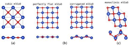
Figure 1.
The with the cubic ( supercell) (a) and monoclinic (c) crystal structure, top and side view (following Ref. [14]). Freestanding perfectly flat and corrugated monolayer crystal structure (b) (following Ref. [18]). Blue denote atoms, red is atoms. The figures are on the same spatial scale.
The description of the electronic structure of systems is also far from being complete—the authors were able to find some data in Ref. [18,20], but no more than that. Besides, at the moment the authors are not aware of any works where a minimal model has been formulated neither for an isolated perfectly flat monolayer , nor for more complex crystal structures such as the corrugated monolayer, monolayer on a substrate or monolayer as an interface. Thus, it seems necessary to obtain on a more systematic basis the densities of states, the band structures and the Fermi surfaces for all listed monolayer systems and to formulate a minimal model for them with the corresponding Hamiltonian parameter values.
In this work, we solve a task of proposing and comparing different minimal models for the monolayer systems as a necessary first step of any further theoretical investigations.
2. Crystal Structure and Calculation Details
To calculate the band structure, the density of states (DOS) and the Fermi surface, we used the density functional theory with the full-potential linear augmented plane-wave framework, as implemented in WIEN2k [21] together with the generalized gradient approximation by Perdew, Burke and Ernzerhof [22], to the exchange-correlation functional.
Figure 2 shows the crystal structures of the systems discussed in this paper. The flat monolayer space group is a 123 (P4/mmm). The lattice parameter is Å [18]. Atoms occupy the following positions: 1a and 1c . We used a 20 Bohr vacuum gap. In order to construct the corrugated monolayer, we doubled the unit cell and made these new additional and atoms unequivalent to the original ones by applying a small shift about 0.5 Bohr in z direction only for them. Resulting system has 59 (Pmmn) [origin choice 2] space group. Next, we did a set of structural relaxations with 10, 20 and 40 Bohr vacuum gaps. There was no difference between 20 and 40 Bohr vacuum gap cases, so in all further calculations we used the 20 Bohr gap. After relaxation neighboring atoms shifted in z direction about Å relative to their original positions, while neighboring atoms barely shifted at all. Since the final corrugated structure of monolayer has a doubled unit cell and is rotated by relative to the flat , we cannot directly compare their calculated electronic structures. Thus, we use additional system—the flat with a doubled (and rotated) unit cell—in order to make a proper comparison. Moreover, for the flat we did a rotation of a local coordinate system in order to use a typical orbital convention, such as in cuprate compounds.
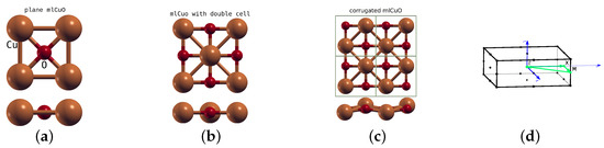
Figure 2.
The flat (a), the with a doubled unit cell (b), the corrugated ( supercell) (c) crystal structures considered in this work, top and side view; brown denote atoms, red is atoms. Brillouin zone for the doubled unit cell and corrugated (d).
All calculations were nonmagnetic and converged self-consistently on a grid of 24 × 24 × 1 k-points in the irreducible Brillouin zone using the Monkhorst-Pack method [23]. We used energy convergence limit 0.1 mRy, force convergence limit 0.5 mRy/a.u. for optimization, , , energy separation Ry. In Figure 2d, we show the Brillouin zone with the k-path used in the band structure analysis.
3. Results and Discussion
3.1. Electronic Structure
Figure 3 shows the DFT (GGA) band structures, the densities of states, bands with their orbital characters and the Fermi surfaces. The first row (a–c) of Figure 3 shows the results for the flat . The band structure in Figure 3a shows that there is an isolated set of bands in the range from eV to eV resembling typical -based HTSC . It has only the - and the - states. The electronic bands of the flat at the Fermi level are formed by the - states (with small addition of the hybrid - states) in consistence with the known results [11]. Note that there is a second band that almost crosses the Fermi level—it is only 0.02 eV lower. It includes the - states hybridized with the -. The Fermi surface has a hole pocket around the X point.
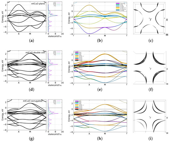
Figure 3.
DFT (GGA) calculated DOS, the band structures, the band structures with the orbital characters and the Fermi surface of the flat (a–c), the with a doubled unit cell (d–f), the corrugated (g–i). Zero corresponds to the Fermi level.
The second row (d–f) of Figure 3 shows the results for the with a doubled unit cell. Due to rotation of a unit cell, its band structure differs from that of the flat in a much more complex way than simply by a large number of bands. The two bands crossing the Fermi level originate from two atoms in the unit cell. They are formed by the - states. Regarding them, we can note degeneracy lifting in the direction. As in the flat , there are the - states (four bands) just below the Fermi level. The Fermi surface has two hole pockets around the M point.
The third row (g–i) of Figure 3 shows the results for the corrugated . Its electronic structure is rather similar to that in the with a doubled unit cell, but there are two notable differences. First, a significant shift of the - bands to eV. Second, a noticeably larger degeneracy lifting for the - bands in the direction. On top of that, the corrugated total energy turns out to be lower than the flat one by eV. In other words, the corrugated state appears to be more favorable and if we have the flat as a topmost layer of some surface, it will most likely be corrugated.
Seeing such a significant shift of the - bands of the corrugated , we wondered if it was possible to raise these states to the Fermi level only via the lattice strain. Significant lattice strain is observed at all sorts of interfaces where there is a mismatch between the lattice parameters. Besides, as we already mention, the corrugated state appears to be more energetically favorable.
To clarify this issue, we carried out a series of calculations where we varied the lattice parameter a from 0% to 10% for the flat and from 0% to 35% for the corrugated . The corresponding results can be observed in Figure 4. For the flat , the lattice deformation leads to a topological Lifshitz transition with the appearance of a new hole pocket around the X point. Clearly, it is a very minor lattice parameter change of the order of experiment accuracy. For the corrugated monolayer, such a transition requires a much larger lattice deformation; it appears only at . Of course, such a strain is too large, and we bring it here only as an illustration. However, for the corrugated case, we want to note a presence of what seems to be a flat band in the direction near the Fermi level. It is likely that a flat band at the Fermi level can be obtained using a reasonable lattice strain and a hole doping.
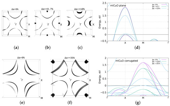
Figure 4.
DFT (GGA) calculated Fermi surface with (zero strain), , and the band structure comparison for the flat (a–d); the Fermi surface with (zero strain), and the band structure comparison for the corrugated (e–g). Zero corresponds to the Fermi level.
Let us now return to the idea we proposed in the introduction: the corrugated of can be described as a transitional system in between the with the cubic and monoclinic structures (Figure 1). Table 1 shows - and - distances in the bulk systems and the monolayers. In the bulk with the cubic structure, layers are significantly stretched—by about relative to the flat , which is close to the considered lattice strain (Figure 4c). We studied the monolayer made from the bulk by simply adding a vacuum between layers (getting slab+vacuum) in z direction and using no relaxation (Figure 1a). The final crystal and band structures were nearly identical to the flat ones with lattice strain (as in Figure 4c,d); thus, we do not include them.

Table 1.
- and - distances in the bulk and the monolayer systems.
There are more surprising results for the bulk with the monoclinic structure. Its layers are also stretched, but to a noticeably lesser extent—by about relative to the corrugated . Its crystal structure has more pronounced corrugation pattern as compared to the corrugated (Figure 1c). To calculate the monoclinic monolayer, we again made a slab+vacuum in z direction and used no relaxation; moreover, we did a rotation of a local coordinate system to remain consistency with the orbital convention chosen for the corrugated . The final space group was 13 (P2/c). The results are given in Figure 5. The most surprising result is that the monoclinic has the band gap at the Fermi level, which opens because of symmetry lowering without using DFT+U or hybrid potentials, as (but for the bulk compound) in Ref. [4,11]. There are mainly the - (with the hybrid -) states near the Fermi level similar to the corrugated . However, it is rather difficult to compare these results in detail with the results for the corrugated (Figure 3g,h) due to the different space group. Let us conclude here that a more complex corrugation pattern leads to a more complex bands structure.
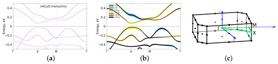
Figure 5.
DFT (GGA) calculated band structure, the band structure with the orbital characters and the corresponding Brillouin zone (a–c) of the monoclinic . Zero corresponds to the Fermi level.
3.2. Minimal Models
The next step in our study is to reveal a good minimal model for both flat and corrugated . In order to do that, we constructed a set of models using the maximally localised Wannier functions (MLWF) within wannier90 package [24]. We examined the following set of models: single-band model with Wannier projected -, three-band model with -, five-band model with -, - and eight-band model with -d, -p. The corresponding band structures are depicted in Figure 6. Note that there are actually twice the number of bands for the corrugated and the with a doubled unit cell due to unit cell doubling in contrast to the flat . The eight-band model resulting band structure is in the excellent agreement with GGA calculated one; in other cases, the agreement is fine at the Fermi level. Thus, the single-band - model for the flat and the corrugated can be used as a minimal model.
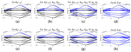
Figure 6.
Comparison DFT (GGA) band structure with a Wannier projected one: - (a), - (b), -, - (c), -d, -p (d) for the with a doubled unit cell; same for the corrugated (e–h). Zero corresponds to the Fermi level.
We also present on-site energies and hopping integrals for one- and three-band models for the flat (Table A1), the corrugated and the with a doubled unit cell (Table A2 and Table A3). The corresponding hopping schemes are illustrated in Figure 7. We used hoppings up to the second coordination sphere for the flat and up to the fifth coordination sphere for the corrugated one. These numbers of neighbors are the minimum required to obtain good agreement between the model Hamiltonian band structure and the initial one. We also attach the values of the Hamiltonian matrix elements in a real space for all the models (Figure 6) as machine-readable data files to Supplementary Materials. So, depending on a task, an interested reader can use the Hamiltonian of the appropriate complexity.
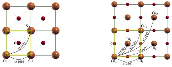
Figure 7.
Hoppings schemes for the flat (left) and the with a doubled unit cell (right). A supercell is displayed for both structures. Yellow transparent square denotes a single unit cell.
4. Conclusions
We investigated the electronic properties of the flat and the corrugated monolayers—DOS, the band structures and the Fermi surfaces. The flat is similar to the bulk with the monoclinic crystal structure and typical -based HTSC, e.g., and has the - states at the Fermi level (with a small addition of the hybrid - states). There is a second band just below the Fermi level—that it is only 0.02 eV lower. It includes the - states hybridized with -.
The corrugation effect leads to a significant shift of the - bands to eV and a degeneracy lifting for the - bands. The corrugated is energetically more favorable than the flat one by eV and is more likely formed as a topmost layer on some surfaces.
It is possible to create a topological Lifshitz transition via lattice strain: for the flat , a slight stretching of the lattice parameter already leads to the appearance of a hole pocket around the X point; this effect for the corrugated occurs at . It is interesting to note the presence of what seems to be a rather flat band in the direction near the Fermi level. Probably, it will be possible to create it using a reasonable strain and a hole doping.
There is a significant mismatch in the lattice parameters of the considered monolayers and the known bulk systems (with the cubic and the monoclinic crystal structures). We conclude that layers in the bulk are stretched relative to the monolayer systems—by about % (cubic bulk vs. flat monolayer) and by % (monoclinic bulk vs. corrugated monolayer). The monolayer made from experimental bulk with the monoclinic crystal structure turns out to have the band gap in our DFT calculation without using DFT+U or hybrid potentials. Clearly, the reason for this is the more complex corrugation patterns of its crystal structure.
We also suggested a set of minimal models for the flat and the corrugated monolayers. The simplest model includes only the - states and agrees well with the GGA calculated band structure at the Fermi level (the latter is also correct for the other models). For the one- and three-band models, we obtained the values of the corresponding Hamiltonian matrix elements in a real space; therefore, depending on the needs, the Hamiltonian of the appropriate complexity can be used.
Before proceeding to more complex systems, such as a monolayer on a substrate or a monolayer as an interface, it was necessary to perform calculations for the original system and understand the features of its electronic structure. So, the next step might be the investigation of such complex systems or using more advanced methods such as DFT+DMFT.
Supplementary Materials
The following supporting information can be downloaded at: https://www.mdpi.com/article/10.3390/ma16020658/s1.
Author Contributions
Conceptualization, I.A.N., M.M.K. and S.G.O.; calculations, A.A.S. and L.V.B.; writing, A.A.S. and I.A.N.; review and editing, I.A.M., M.M.K. and S.G.O.; funding acquisition, I.A.N. All authors have read and agreed to the published version of the manuscript.
Funding
This research was in part funded by the Russian Science Foundation grant number 23-22-00372.
Acknowledgments
L.V.B. would like to thank the Irkutsk Supercomputer Center of SB RAS for providing the access to HPC-cluster «Akademik V.M. Matrosov» (Irkutsk Supercomputer Center of SB RAS, Irkutsk: ISDCT SB RAS; http://hpc.icc.ru, accessed 21 November 2022).
Conflicts of Interest
The authors declare no conflict of interest. The funders had no role in the design of the study; in the collection, analyses, or interpretation of data; in the writing of the manuscript; or in the decision to publish the results.
Appendix A
We attach the values of the Hamiltonian matrix elements of all the models considered in this work as Supplementary Materials. These are machine-readable data files with self-explanatory names and some comments.
Table A1.
An on-site energies and hoppings in meV for the flat (one- and three-band models).
Table A1.
An on-site energies and hoppings in meV for the flat (one- and three-band models).
| - | - | |||||
|---|---|---|---|---|---|---|
| 126 | 169 | |||||
| 226 | ||||||
| 0 | 0 | |||||
Table A2.
An on-site energies and hoppings in meV for the doubled unit cell and corrugated (one-band model).
Table A2.
An on-site energies and hoppings in meV for the doubled unit cell and corrugated (one-band model).
| - | ||||||
|---|---|---|---|---|---|---|
| Doubled u.c. | Corrugated | |||||
| 124 | 73 | 161 | 86 | |||
| 13 | 5 | |||||
Table A3.
An on-site energies and hoppings in meV for the doubled unit cell and corrugated (three-band model).
Table A3.
An on-site energies and hoppings in meV for the doubled unit cell and corrugated (three-band model).
| - | ||||||
|---|---|---|---|---|---|---|
| Doubled u.c. | Corrugated | |||||
| 167 | 82 | 24 | 85 | |||
| 10 | ||||||
| 0 | 0 | 0 | 0 | 30 | ||
| 0 | 0 | 0 | 41 | 31 | 31 | |
| 0 | 0 | 0 | 41 | 7 | ||
| 0 | 0 | 0 | 34 | |||
| 18 | 41 | 5 | 0 | 14 | 14 | |
| 53 | 43 | |||||
| 18 | 5 | 4 | 4 | |||
| 0 | 0 | 47 | 0 | 0 | 28 | |
| 2 | ||||||
| 246 | 206 | |||||
References
- Anisimov, V.I.; Zaanen, J.; Andersen, O.K. Band theory and Mott insulators: Hubbard U instead of Stoner I. Phys. Rev. B 1991, 44, 943–954. [Google Scholar] [CrossRef] [PubMed]
- Ruiz, E.; Alvarez, S.; Alemany, P.; Evarestov, R.A. Electronic structure and properties of Cu2O. Phys. Rev. B 1997, 56, 7189–7196. [Google Scholar] [CrossRef]
- Ghijsen, J.; Tjeng, L.H.; van Elp, J.; Eskes, H.; Westerink, J.; Sawatzky, G.A.; Czyzyk, M.T. Electronic structure of Cu2O and CuO. Phys. Rev. B 1998, 38, 11322–11330. [Google Scholar] [CrossRef] [PubMed]
- Heinemann, M.; Eifert, B.; Heiliger, C. Band structure and phase stability of the copper oxides Cu2O, CuO, and Cu4O3. Phys. Rev. B 2013, 87, 115111. [Google Scholar] [CrossRef]
- Pickett, W.E. Electronic structure of the high-temperature oxide superconductors. Rev. Mod. Phys. 1989, 61, 433–512. [Google Scholar] [CrossRef]
- Reitz, J.B.; Solomon, E.I. Propylene Oxidation on Copper Oxide Surfaces: Electronic and Geometric Contributions to Reactivity and Selectivity. J. Am. Chem. Soc. 1998, 120, 11467–11478. [Google Scholar] [CrossRef]
- Nakaoka, K.; Ueyama, J.; Ogura, K. Photoelectrochemical Behavior of Electrodeposited CuO and Cu2O Thin Films on Conducting Substrates. J. Electrochem. Soc. 2004, 151, C661. [Google Scholar] [CrossRef]
- Kim, S.Y.; Ahn, C.H.; Lee, J.H.; Kwon, Y.H.; Hwang, S.; Lee, J.Y.; Cho, H.K. p-Channel Oxide Thin Film Transistors Using Solution-Processed Copper Oxide. ACS Appl. Mater. Interfaces 2013, 5, 2417–2421. [Google Scholar] [CrossRef]
- Åsbrink, S.; Norrby, L.J. A refinement of the crystal structure of copper(II) oxide with a discussion of some exceptional e.s.d.’s. Acta Crystallogr. Sect. B 1970, 26, 8–15. [Google Scholar] [CrossRef]
- Schmahl, N.G.; Eikerling, G.F. Über Kryptomodifikationen des Cu(II)-Oxids. Z. Für Phys. Chem. 1968, 62, 268–279. [Google Scholar] [CrossRef]
- Ekuma, C.; Anisimov, V.; Moreno, J.; Jarrell, M. Electronic structure and spectra of CuO. Eur. Phys. J. B 2014, 87, 23. [Google Scholar] [CrossRef]
- Wu, D.; Zhang, Q.; Tao, M. LSDA+U study of cupric oxide: Electronic structure and native point defects. Phys. Rev. B 2006, 73, 235206. [Google Scholar] [CrossRef]
- Nolan, M.; Elliott, S.D. The p-type conduction mechanism in Cu2O: A first principles study. Phys. Chem. Chem. Phys. 2006, 8, 5350–5358. [Google Scholar] [CrossRef] [PubMed]
- Cao, H.; Zhou, Z.; Yu, J.; Zhou, X. DFT study on structural, electronic, and optical properties of cubic and monoclinic CuO. J. Comput. Electron. 2018, 17, 21–28. [Google Scholar] [CrossRef]
- Grant, P.M. Electronic properties of rocksalt copper monoxide: A proxy structure for high temperature superconductivity. J. Phys. Conf. Ser. 2008, 129, 012042. [Google Scholar] [CrossRef]
- Cipriano, L.A.; Di Liberto, G.; Tosoni, S.; Pacchioni, G. Band Gap in Magnetic Insulators from a Charge Transition Level Approach. J. Chem. Theory Comput. 2020, 16, 3786–3798. [Google Scholar] [CrossRef] [PubMed]
- Yazdani, A.; Barakati, B. A first-principles study on electronic structure and crystal field effect of layered La2CuO4 as composed of CuO2 and La2O2 monolayers. Phys. E Low-Dimens. Syst. Nanostructures 2021, 125, 114395. [Google Scholar] [CrossRef]
- Yin, K.; Zhang, Y.Y.; Zhou, Y.; Sun, L.; Chisholm, M.F.; Pantelides, S.T.; Zhou, W. Unsupported single-atom-thick copper oxide monolayers. 2D Mater. 2016, 4, 011001. [Google Scholar] [CrossRef]
- Kano, E.; Kvashnin, D.G.; Sakai, S.; Chernozatonskii, L.A.; Sorokin, P.B.; Hashimoto, A.; Takeguchi, M. One-atom-thick 2D copper oxide clusters on graphene. Nanoscale 2017, 9, 3980–3985. [Google Scholar] [CrossRef]
- Kvashnin, D.G.; Kvashnin, A.G.; Kano, E.; Hashimoto, A.; Takeguchi, M.; Naramoto, H.; Sakai, S.; Sorokin, P.B. Two-Dimensional CuO Inside the Supportive Bilayer Graphene Matrix. J. Phys. Chem. C 2019, 123, 17459–17465. [Google Scholar] [CrossRef]
- Blaha, P.; Schwarz, K.; Tran, F.; Laskowski, R.; Madsen, G.K.H.; Marks, L.D. WIEN2k: An APW+lo program for calculating the properties of solids. J. Chem. Phys. 2020, 152, 074101. [Google Scholar] [CrossRef] [PubMed]
- Perdew, J.P.; Burke, K.; Ernzerhof, M. Generalized Gradient Approximation Made Simple. Phys. Rev. Lett. 1996, 77, 3865–3868. [Google Scholar] [CrossRef] [PubMed]
- Monkhorst, H.J.; Pack, J.D. Special points for Brillouin-zone integrations. Phys. Rev. B 1976, 13, 5188. [Google Scholar] [CrossRef]
- Pizzi, G.; Vitale, V.; Arita, R.; Blügel, S.; Freimuth, F.; Géranton, G.; Gibertini, M.; Gresch, D.; Johnson, C.; Koretsune, T.; et al. Wannier90 as a community code: New features and applications. J. Phys. Condens. Matter. 2020, 32, 165902. [Google Scholar] [CrossRef] [PubMed]


Disclaimer/Publisher’s Note: The statements, opinions and data contained in all publications are solely those of the individual author(s) and contributor(s) and not of MDPI and/or the editor(s). MDPI and/or the editor(s) disclaim responsibility for any injury to people or property resulting from any ideas, methods, instructions or products referred to in the content. |
© 2023 by the authors. Licensee MDPI, Basel, Switzerland. This article is an open access article distributed under the terms and conditions of the Creative Commons Attribution (CC BY) license (https://creativecommons.org/licenses/by/4.0/).