Abstract
This paper investigates the bipolar resistive switching and synaptic characteristics of IZO single-layer and IZO/SiO2 bilayer two-terminal memory devices. The chemical properties and structure of the device with a SiO2 layer are confirmed by x-ray photoemission spectroscopy (XPS) and transmission electron microscopy (TEM) imaging. The device with the SiO2 layer showed better memory characteristics with a low current level, as well as better cell-to-cell and cycle-to-cycle uniformity. Moreover, the neuromorphic applications of the IZO/SiO2 bilayer device are demonstrated by pulse response. Paired pulse facilitation, excitatory postsynaptic current, and pulse-width-dependent conductance changes are conducted by the coexistence of short- and long-term memory characteristics. Moreover, Hebbian rules are emulated to mimic biological synapse function. The result of potentiation, depression, spike-rate-dependent plasticity, and spike-time-dependent plasticity prove their favorable abilities for future applications in neuromorphic computing architecture.
1. Introduction
To overcome the scaling issue of present complementary metal-oxide-semiconductor (CMOS) technology and the bottleneck problem of Von Neumann computing architecture, various next-generation memory devices to implement neuromorphic computing architecture have emerged in recent years [1,2,3,4,5,6]. Because of its easy fabrication method, high switching speed, low operating voltage, and non-volatility, resistive random-access memory (RRAM) is regarded as the most promising choice for the next generation of memory [7,8,9,10,11,12,13,14,15,16,17,18,19]. Furthermore, several structures expandable to high density, such as 3D vertical structures and array structures, are easy to use due to their simple metal–insulator–metal structures [20,21,22,23,24,25,26,27].
The resistive switching phenomena of metal-oxide-based RRAM of the bipolar switching type are caused by the creation and rupture of a conducting filament in the insulating layer that connects the top and bottom electrodes [28,29,30,31,32,33,34,35,36]. When the conducting filament links the top and bottom electrodes under external voltage bias, a large current flows with decreasing resistance. Thus, the device switches from its initial resistance state to a low-resistance state (LRS), indicating the device is ‘on’. Alternatively, when an opposite polarity bias is employed, it causes a break in the conducting path, restricting the flow of the current and transitioning the device into a state of high resistance (HRS), effectively turning it ‘off’. Various metal oxides such as TaOx [37], ZrO2 [38], ZnO [39,40], SiO2 [41,42], and HfOx [43] have been widely studied for resistive switching. Uniformity poses a significant challenge in metal-oxide-based RRAM because of the sporadic creation and disruption of conducting filaments. One way to improve uniformity is by inserting a thin SiO2 layer, which prevents hard breakdown and enables repeated switching [44]. Among these, ZnO is gathering interest due to the suitable range of its bandgap (~3.37 eV at 300K) for resistive switching [45], good transparency [46], and abundant defects [47] for memory applications. Also, indium zinc oxide (IZO) is a popular semiconductor material applied in various devices such as thin film transistors (TFT) [48,49], oxide diodes [50], and sensors [51] due to its high thermal stability, low film stress, and high transparency [52,53,54]. However, most of the IZO applications in RRAM involve making transparent electrodes [55,56]. Although Hsu et al. discovered a bipolar resistive switching phenomenon in sol–gel IZO, its synaptic applications can be investigated further [57].
In this paper, we fabricated an IZO layer-based RRAM device using RF sputtering. Thin silicon oxide was introduced between the bottom electrode and the IZO layer to improve its resistive switching properties. In addition to an improvement in uniformity, the current level was reduced, improving its power consumption. Furthermore, the synaptic characteristics of the ITO/IZO/SiO2/TaN bilayer device were characterized by applying a pulse on the device. Due to the coexistence of short- and long-term memory characteristics, potentiation, depression, paired-pulse facilitation (PPF), and excitatory postsynaptic current (EPSC) were performed [58,59,60,61,62]. Finally, spike-rate-dependent plasticity (SRDP) and spike-time-dependent plasticity (STDP) of the Hebbian rule were emulated to investigate the ability of ITO/IZO/SiO2/TaN (tantalum nitride) stack to act as a synapse device [63,64,65].
2. Experimental Section
To fabricate the RRAM device, a SiO2/Si wafer was cleaned using acetone and isopropyl alcohol (IPA). Subsequently, a TaN bottom electrode with a thickness of 100 nm was sputtered onto the SiO2/Si wafer using DC sputtering. A Ta target of 99.99% purity was employed at a DC power of 65 W. The sputtering gas was a mixed gas of Ar (19 sccm) and N2 (1 sccm) with a deposition pressure of 5 mTorr. Next, for the IZO/SiO2 bilayer device, on top of the TaN layer, SiO2 was deposited using low-pressure chemical vapor deposition (LPCVD). The deposition occurred at 785 °C by reacting dichlorosilane (DCS, SiCl2H2, 40 sccm) and N2O (160 sccm). Then, for both devices, IZO 50 nm thick was deposited through a radio frequency (RF) sputter, with an RF power of 50 W. The deposition pressure was 2 mTorr, and the reactive gas consisted of Ar 10 sccm and O2 1 sccm. Following the deposition of the IZO film, square patterns measuring 100 µm × 100 µm were created using photolithography. Subsequently, a indium tin oxide (ITO) top electrode 120 nm thick was deposited and shaped through a lift-off process using acetone after the RF sputter deposition of ITO, which employed a commercial ITO target of 99.99% purity, operated at an RF power of 80 W. The gas pressure stood at 3 mTorr with an Ar flow of 8 sccm. The electrical characteristics of both devices were assessed using the Keithley 4200-SCS semiconductor parameter analyzer and the 4225-PMU pulse measurement unit from Keithley Instruments in Cleveland, OH, USA. The bias was applied to the top electrode (ITO), while the bottom electrode (TaN) remained grounded. Additionally, the device’s schematic and its chemical properties were examined using X-ray photoelectron spectroscopy (XPS) and transmission electron microscopy (TEM) (Oxford Instruments, Tubney Woods, Abingdon, UK).
3. Results and Discussion
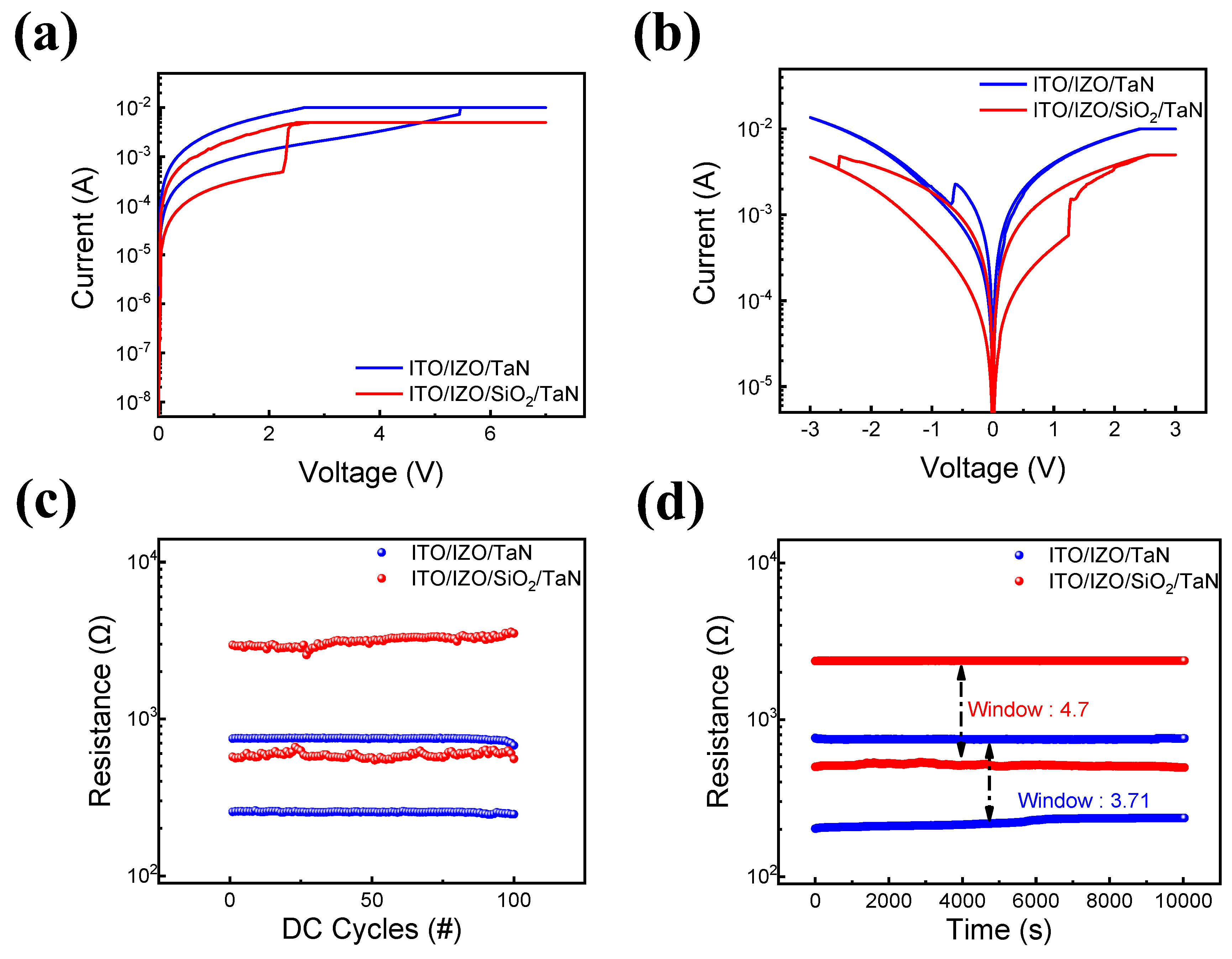
Figure 1 shows the resistive switching characteristics of IZO-based RRAM devices. Figure 1a shows that both ITO/IZO/TaN single-layer and ITO/IZO/SiO2/TaN bilayer devices require a forming process to transition from an initial resistance state to an LRS [63,66]. The forming process is often known as the initial set or breakdown process, accumulating the defects in thin films under a higher voltage applied prior to the resistive switching phenomenon. The forming process is controlled by compliance currents of 10 mA and 5 mA for single-layer and bilayer devices, respectively. The I-V curves of the devices are shown in Figure 1b. Both devices were controlled at less than 3 V and −3 V for the set and reset processes. However, different compliance currents were needed in order to avoid a hard breakdown. For the single-layer IZO device, a high compliance current of 30 mA was needed. However, for the bilayer ITO/IZO/SiO2/TaN device, a relatively lower compliance current of 5 mA is required. The cycle-to-cycle endurance and retention characteristics of both devices were then examined. In Figure 1c,d, it is shown that both devices remained in their LRS and HRS states during 100 endurance cycles and 104 s of retention time, with voltages of 3 and −3 V applied to trigger the resistive switching phenomenon and a read bias of −0.3 V. In both experiments, the bilayer ITO/IZO/SiO2/TaN device had a lower operating current level and a larger window compared to the ITO/IZO/TaN device. This phenomenon can be noted as the effect of inserting a thin SiO2 film, decreasing the on and off currents, and improving the device’s power consumption.
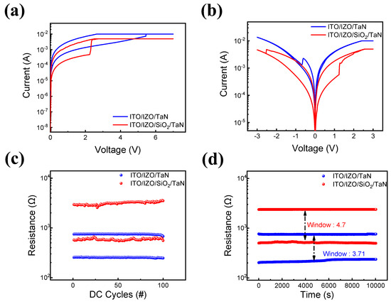
Figure 1.
Resistive switching characteristics of devices with and without an SiO2 layer. (a) I–V curves of forming process; (b) I–V curves of set and reset processes. (c) Endurance characteristics; (d) retention test in HRS and LRS at a read voltage of −0.2 V.
Figure 2 shows the cell-to-cell variations in both devices. A total of 10 randomly selected cells from both devices were selected, and 20 cycles were run for each cell. The addition of a SiO2 layer enhances cell-to-cell and cycle-to-cycle uniformity as illustrated in Figure 2a,b. Figure 2c also depicts the cell-to-cell variability of the ITO/IZO/TaN and ITO/IZO/SiO2/TaN devices. By introducing a SiO2 thin film, the variability of both HRS and LRS was improved.

Figure 2.
Cell-to-cell variance of 10 randomly selected cells of (a) ITO/IZO/TaN device and (b) ITO/IZO/SiO2/TaN device. (c) Calculated cell-to-cell variability of devices with and without an SiO2 layer.
To confirm the fabrication of the bilayer device as shown in the schematic structure in Figure 3a, TEM and XPS were used. A cross-sectional TEM image of the device is shown in Figure 3b. The sputter-deposited ITO and TaN electrodes had thicknesses of 120 nm and 100 nm, respectively. Additionally, insulating layers were sandwiched between the electrodes. The thicknesses of the IZO and SiO2 layers were about 50 nm and 2 nm, respectively. Furthermore, the XPS depth mode is used to investigate the chemical components of the IZO and SiO2 layers, as shown in Figure 4.

Figure 3.
(a) Schematic structure of ITO/IZO/SiO2/TaN device. (b) Cross-sectional TEM images.
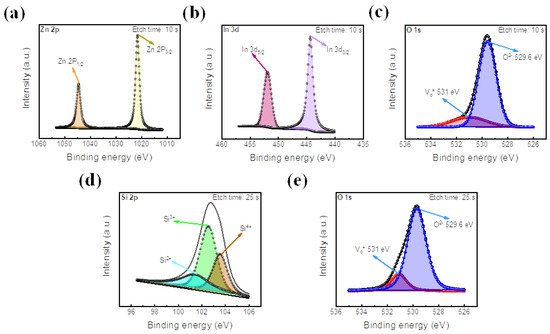
Figure 4.
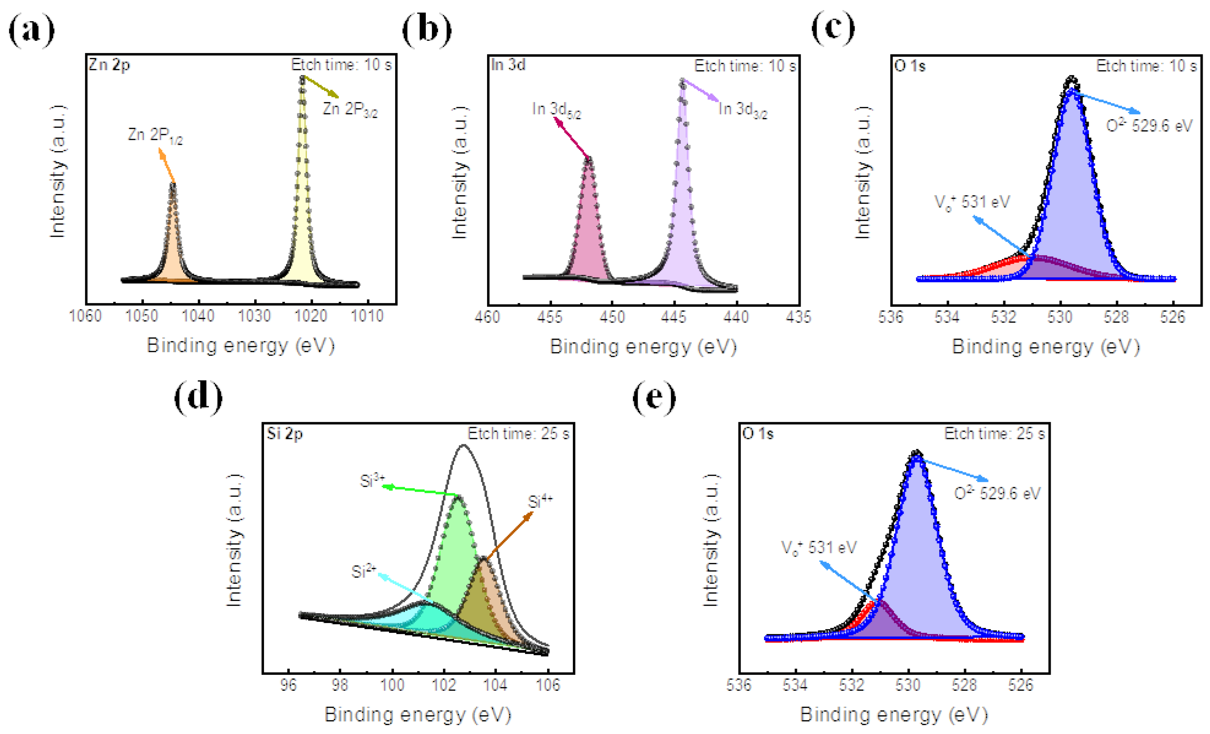
XPS peak analysis of IZO and SiO2 films. (a) Zn 2p peak, (b) In 3d peak, and (c) O 1s peak of IZO film. (d) Si 2p peak and (e) O 1s peak of SiO2 film.
XPS spectra of the IZO film are depicted in Figure 4a–c, with an etch time of 10 s. The peak intensity values of Zn 2p are located at the binding energies of 1021.5 eV and 1045.2 eV for Zn 2p3/2 and 2p1/2, respectively [40]. 3d5/2 and 3d3/2 are located at about 444.6 eV and 453.35 eV, respectively [67]. In addition, as shown in Figure 4c, the peak of O 1s at 529.6 eV represents metal–oxygen bonding, proving the existence of the IZO insulating layer [68]. Next, the Si-O bond is illustrated at an etch time of 25 s, as shown in Figure 4d,e. The XPS of Si 2p is shown to have three peaks, representing its three oxide states of Si2+, Si3+, and Si4+ [69]. Also, the O 1s peak of Figure 4e is located at about 529.6 eV, demonstrating Si-O bonding. Additionally, in both the O 1s peaks of the IZO and SiO2 thin films, an additional peak is located at a binding energy of 531 eV, which represents the existence of oxygen vacancies in each insulating layer [34].
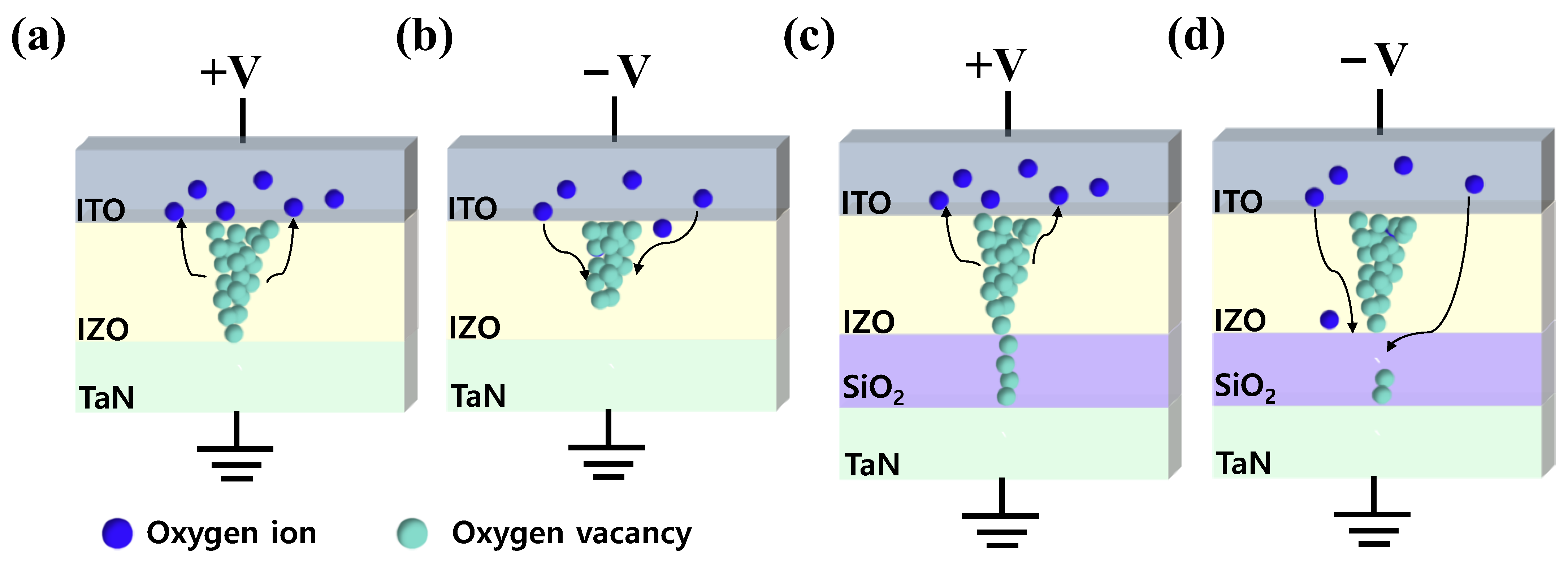
Illustrations of resistive switching mechanisms are shown in Figure 5. For an ITO/IZO/TaN device, when a positive bias is applied to the top electrode, oxygen ions in the IZO film migrate toward the ITO layer via the electric field, where the ITO layer acts as an oxygen reservoir. Then, the amount of oxygen vacancies in the IZO film increases and forms a thick conducting filament, enabling a large current flow in the device. As a result, a set occurs, and the device switches to LRS (Figure 5a). Moreover, when the opposite bias is applied to the top electrode, oxygen ions stored in the ITO layer return to the IZO film and recombine with oxygen vacancies. Thus, a reset occurs due to the rupture of a conducting filament, and the device switches into HRS (Figure 5b). However, due to the random nature of the conducting filament, the single-layer device suffered from poor uniformity. On the other hand, for the ITO/IZO/SiO2/TaN device, when a positive bias was applied to the top electrode as shown in Figure 5c, oxygen vacancies generated in the IZO-film accumulated and formed a conical-shaped filament toward the interface of IZO/SiO2 [70,71], making the IZO film more conductive [72]. During the formation of the filament, a major drop in electric potential occurred in the SiO2 film. A high electric field was applied to the film, localizing the conducting filament and reducing randomness in the formation of the conducting path [44]. Additionally, the reduced current levels were likely achieved due to the narrow thickness of the conducting path in the SiO2 film, limiting the current flow. Furthermore, it is believed that when a negative voltage is applied to the top electrode, as illustrated in Figure 5d, the rupture of the conducting filament occurs in the SiO2 layer, where, due to its diffusion limiting role, an improvement in uniformity occurs [73,74].
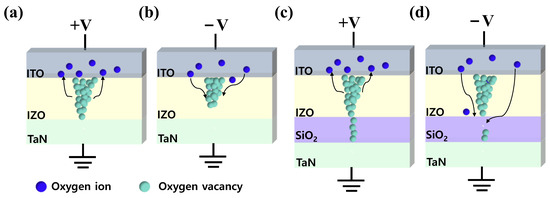
Figure 5.
Conduction mechanism of the ITO/IZO/TaN device, (a) Set, and (b) Reset. Conduction mechanism of the ITO/IZO/SiO2/TaN device, (c) Set, and (d) Reset.
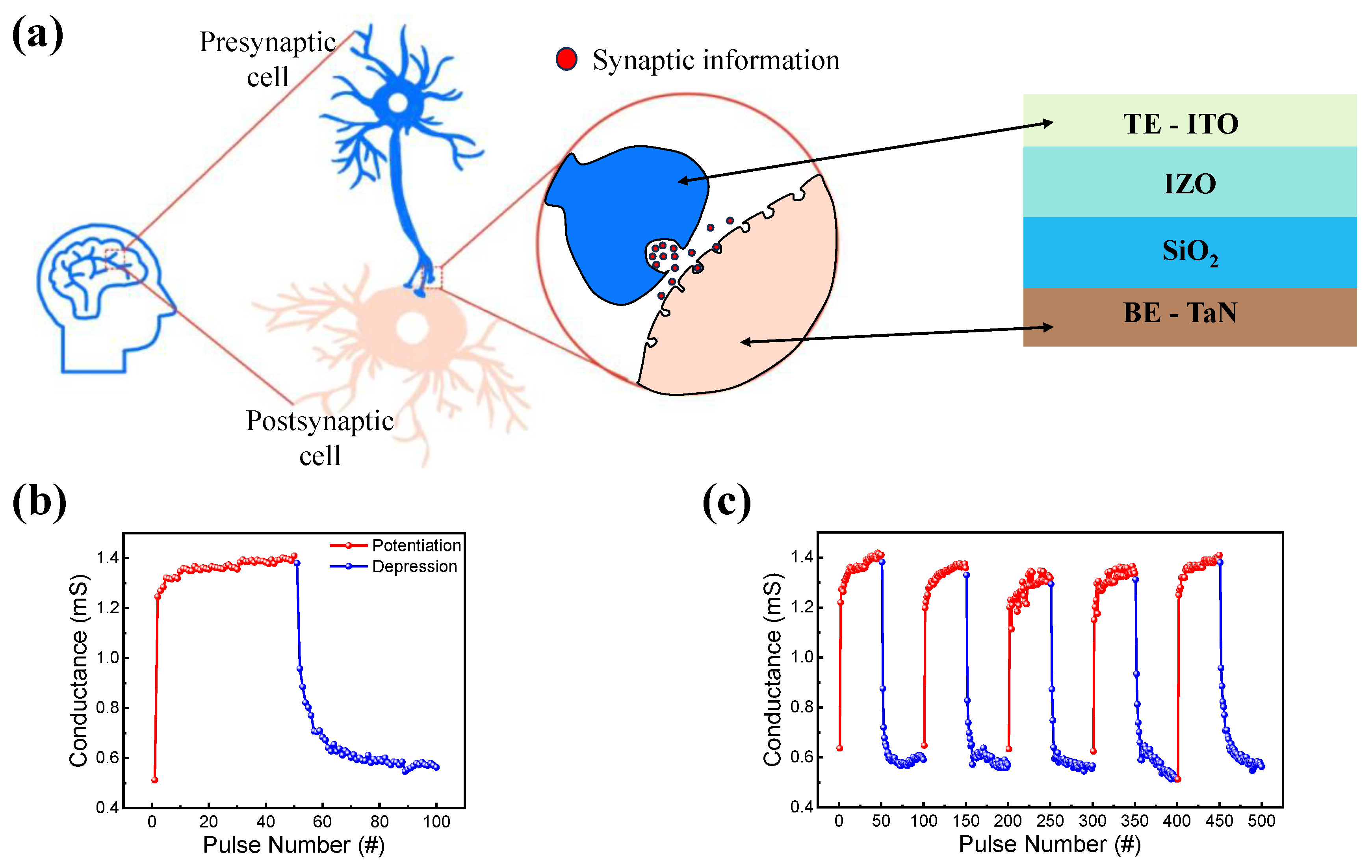
In a biological synapse, synaptic information is processed through neurons. As shown in Figure 6a, neurons are composed of pre- and post-synaptic cells, which can be easily mimicked by a two-terminal RRAM device. As a synaptic device, the top and bottom electrodes mimic pre- and post-synaptic cells. One of the important features of neuromorphic application is potentiation and depression [75]. A pulse train of 50 identical set and reset pulses were used for potentiation and depression. The amplitude and width of the set pulses were 2 V and 0.5 μs, and those of the reset pulse were −1.5 V and 5 μs. Figure 6b shows the increase and decrease in conductance caused by the pulse trains. Five potentiation and depression cycles were also performed to ensure reproducibility, as shown in Figure 6c.
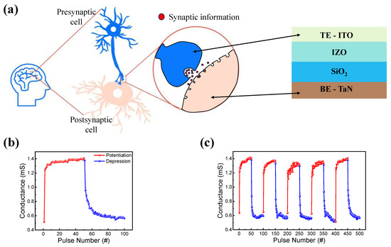
Figure 6.
(a) Schematic of an RRAM device as a synaptic device and a biological synapse. (b) Potentiation and depression. (c) Five cycles of repetition of potentiation and depression.
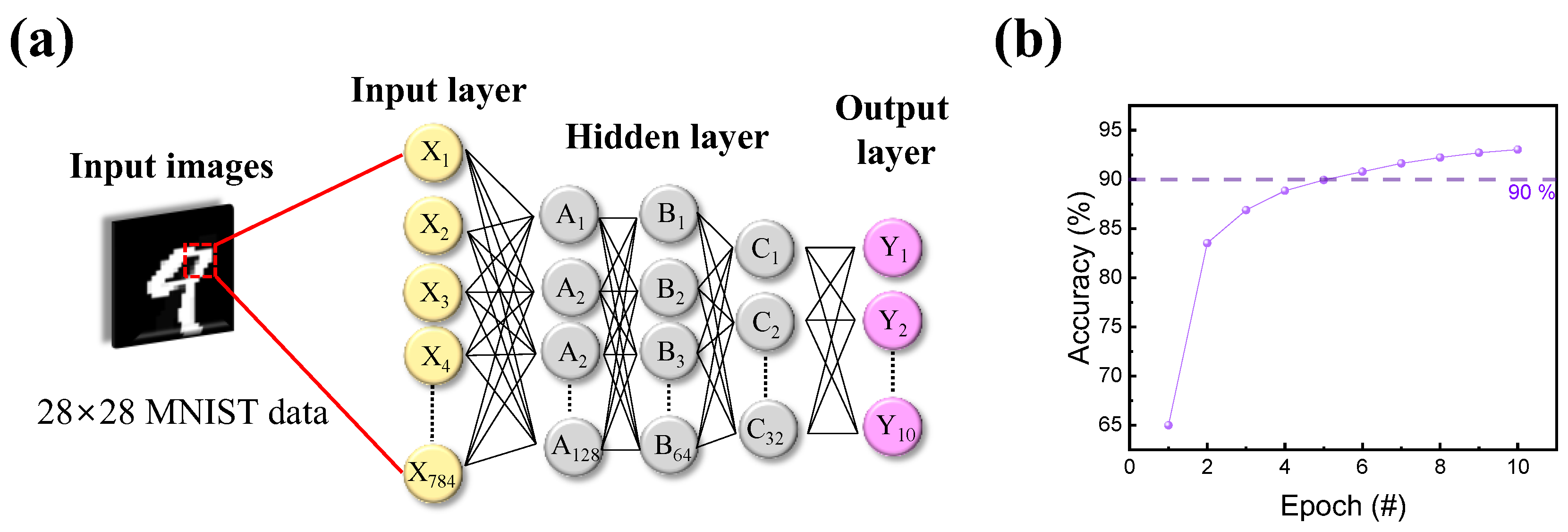
The results of potentiation and depression were then transformed into an artificial neural network to calculate the accuracy of a Modified National Institute of Standards and Technology (MNIST) handwritten data set. As illustrated in Figure 7a, the deep neural network-based pattern recognition system (PRS) consisted of input, hidden, and output layers. When the 28 × 28-pixel MNIST handwritten data set entered, nodes of layers changed their parameters via the backpropagation method. Then, by repeating its training through epochs, the accuracy of PRS improved with the training time. Figure 7b shows the training outcome after 10 successive epochs, with a maximum accuracy of 93.03% [76].
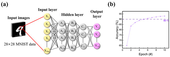
Figure 7.
Pattern recognition through a neural network. (a) Schematic illustration of a deep neural network for numerical number recognition consisting of input, hidden, and output layers. (b) Simulated recognition accuracy using the MNIST numerical data set, with a maximum accuracy of 93.03% for the ITO/IZO/SiO2/ITO device.
Furthermore, in the human brain, short-term memory (STM) and long-term memory (LTM) coexist. This was implemented in the short-term device by rehearsing certain events, and STM could be converted into LTM [77]. Thus, the coexistence of STM and LTM characteristics in RRAM devices is beneficial for synaptic applications. PPF is neural facilitation in biological systems related to short-term synaptic plasticity (STP) [78,79,80]. The STP behavior was replicated in the ITO/IZO/SiO2/TaN device to investigate the coexistence of volatility and non-volatility in one RRAM cell. A twin pulse with an amplitude of 2.6 V and a width of 10 μs was applied to the semiconductor device under a varied pulse interval of 1 μs to 500 μs. The PPF behavior is known to be related to the negative correlation between time interval and PPF index (PPF index = ((I2 − I1)/I1) × 100, where I2 is the current response of the second pulse and I1 is the current response of the first pulse train). When the time between two pulses was short, the device remembered the first stimulus, resulting in a greater current response to the second stimulation. When the gap was long enough, however, the system forgot about the first stimulus and no variation occurred in the second pulse. The result of the twin pulse scheme is illustrated in Figure 8a.

Figure 8.
(a) PPF as a function of time interval. (b) Change in EPSC depending on the number of pulses applied. (c) Pulse-width-dependent conductance change.
Additionally, the EPSC change in the device by varying pulse number was conducted to check whether the ITO/IZO/SiO2/TaN device could convert STM to LTM by repeating the experiment. The pulse amplitude and width were fixed at 2.4 V and 100 μs. The number of pulses varied from 1 to 20. Figure 8b shows that as the number of pulses increased, the EPSC increased, and the read current abruptly surged after 20 consecutive pulses, indicating that the STM was switched to LTM. To further investigate the relationship between pulse width and its current response, the EPSC test was repeated with the pulse width varying from 1 μs to 100 μs, while the pulse amplitude had a fixed value of 2.6 V. The result is shown in Figure 8c, where the linear relationship between pulse and conductance is observed. When the pulse width was short, the STM characteristics remained. On the other hand, when the pulse width was long, long-term potentiation occurred from the first single pulse, resulting in higher conductance at the final 20 consecutive pulses.
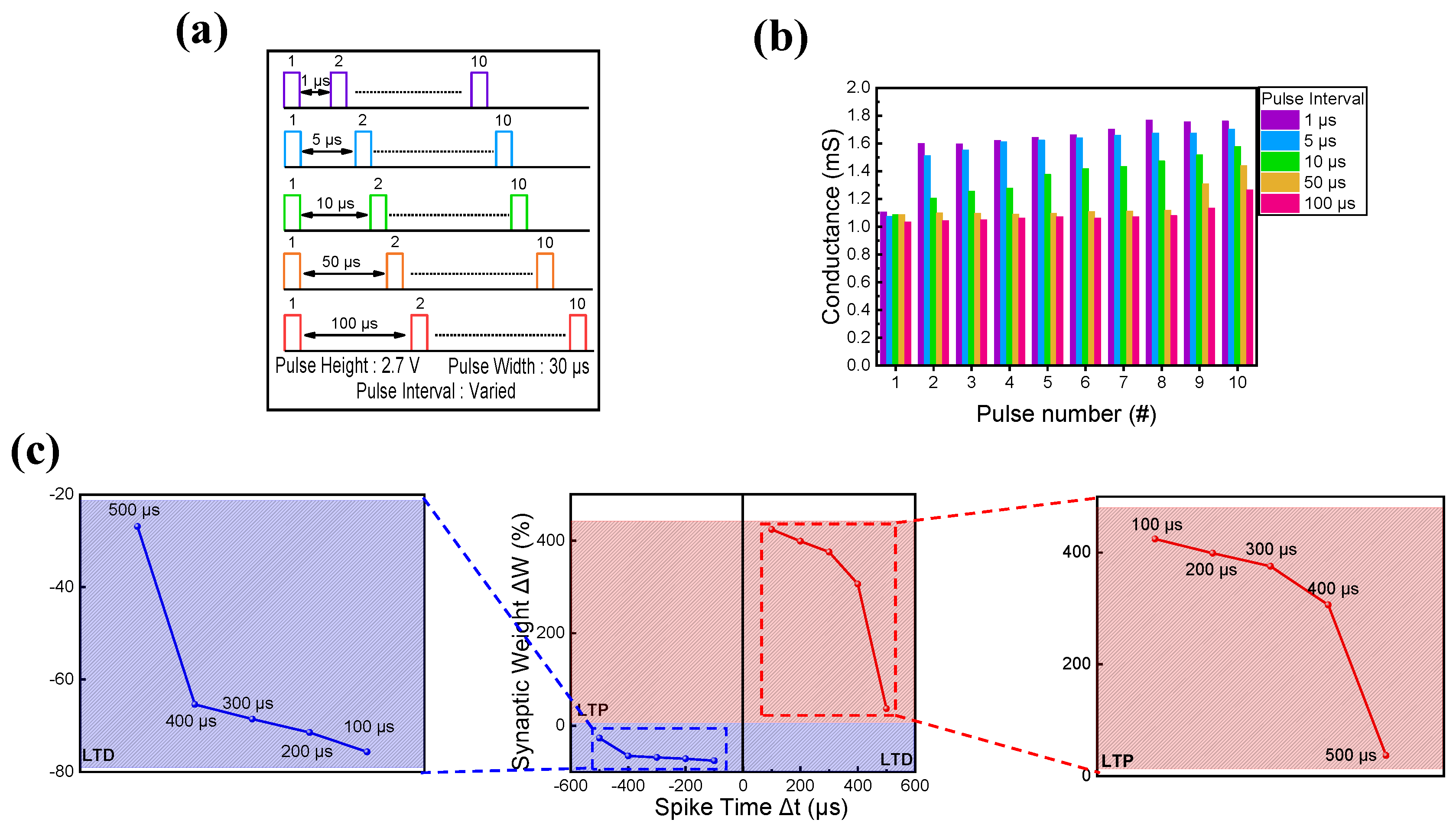
Finally, Hebbian rules were applied to ITO/IZO/SiO2/TaN devices [81]. As the basis of neuromorphic computing implementation is emulating the biological brain, synaptic devices need to mimic the brain’s synapse and neuron properties. In this synapse and neuron interconnection process, various functions occurred under given stimuli, strengthening or weakening the synaptic connection [82]. One of the ways to implement this weight change is by following the Hebbian rules, which are learning tools that verify the ability of the synapse device to imitate the synaptic plasticity of biological synapses. Among various Hebbian rules, SRDP and STDP are two of the most typical ways to copy synaptic weight change and information processing between pre- and post-synaptic cells [83,84,85,86,87]. First, SRDP behavior is observed by altering the pulse interval. The schematic illustration of the pulse train is shown in Figure 9a, where the pulse interval varies from 1 μs to 100 μs. The pulse height and width have fixed values of 2.7 V and 30 μs. In Figure 9b, the SRDP response is illustrated. The pulse interval and conductance value are shown to have a linear relationship. When the pulse interval was short, the synapse received practically consecutive pulse trains, rapidly increasing the conductance. When the pulse interval was long, however, the synapse ‘forgot the previous stimulus, resulting in a gradual increase in conductance. Furthermore, STDP was examined by applying the same pair of pulses to the pre-and post-synapse under varied time difference conditions. Spike time (Δt) was defined as the time difference of pulse trains applied to the pre-and post-synapses (Δt = tpost − tpre. tpost and tpre are the times when pulses are applied to the pre-and post-synapses). If the pre-synapse fired before the post-synapse (Δt > 0), a set of pulses led to LTP. Conversely, if the post-synapse fired before the pre-synapse (Δt < 0), a different set of pulses caused LTD. The STDP behavior of the ITO/IZO/SiO2/TaN device is illustrated in Figure 9c, where the depression of the synaptic weight (ΔW) is shown with an increase in spike time value. Here, ΔW = (Gf − Gi)/Gi) × 100, where Gf is the conductance value of the device after pulse application and Gi is the conductance value of the device before pulse application.

Figure 9.
(a) Schematic illustration of pulses applied to observe SRDP behavior. (b) SRDP and (c) STDP behaviors of ITO/IZO/SiO2/TaN device.
4. Conclusions
In summary, the resistive switching and synaptic properties of IZO-based RRAM devices were investigated by electrical measurements, including DC sweep and pulse response. The bilayer-structured ITO/IZO/SiO2/TaN device demonstrated superior memory characteristics compared to the single-layer device, consuming less power and showing better uniformity. It is noted that the inserted SiO2 layer prevented the hard breakdown of the IZO layer and localized the conducting filament. Additionally, synaptic functions were assessed using pulse measurements and other biological synapse learning criteria. The PPF, potentiation, depression, and EPSC changes demonstrate the coexistence of STM and LTM. Finally, STDP and SRDP prove the potential of the ITO/IZO/SiO2/TaN device to be used in future neuromorphic system applications.
Author Contributions
Conceptualization, M.K. and S.K.; Formal analysis, D.J.; Investigation, D.J.; Writing—original draft, D.J.; Writing—review & editing, M.K. and S.K.; Supervision, M.K. and S.K.; Project administration, M.K. and S.K.; Funding acquisition, S.K. All authors have read and agreed to the published version of the manuscript.
Funding
This work was supported in part by a National Research Foundation of Korea (NRF) grant funded by the Ministry of Science and ICT (Grant No. 2021R1C1C1004422) and by Incheon National University Research Grant in 2020.
Institutional Review Board Statement
Not applicable.
Informed Consent Statement
Not applicable.
Data Availability Statement
Data are contained within the article.
Conflicts of Interest
The authors declare no conflict of interest.
References
- Yuan, L.; Hsieh, K.; Liu, R. Future challenges of flash memory technologies. Microelectron. Eng. 2009, 86, 283–286. [Google Scholar]
- Kim, S.; Kim, H.; Hwang, S.; Kim, M.; Chang, Y.; Park, B. Analog synaptic behavior of a silicon nitride memristor. ACS Appl. Mater. Interfaces 2017, 9, 40420–40427. [Google Scholar] [CrossRef] [PubMed]
- Jang, J.; Ko, D.; Ahn, G.; Yu, H.; Junh, H.; Kim, Y.; Yoon, C.; Lee, S.; Park, B.; Choi, S.; et al. Effect of oxygen content of the LaAlO3 layer on the synaptic behavior of Pt/LaAlO3/Nb-doped SrTiO3 memristors for neuromorphic applications. Solid-State Electron. 2018, 140, 139–143. [Google Scholar] [CrossRef]
- Lelmini, D. Resistive switching memories based on metal oxides: Mechanisms, reliability and scaling. Semicond. Sci. Technol. 2016, 31, 063002. [Google Scholar] [CrossRef]
- Bai, S.; Guo, T.; Zhou, G.; Ranjan, S.; Jiao, Y.; Wei, L.; Zhou, Y.N.; Wu, Y.A. Synaptic devices based neuromorphic computing applications in artificial intelligence. Mater. Today Phys. 2021, 18, 100393. [Google Scholar]
- Kim, M.; Lee, J. Short-term plasticity and long-term potentiation in artificial synapse with diffusive dynamics. ACS Nano 2018, 12, 1680–1687. [Google Scholar] [CrossRef] [PubMed]
- Waser, R.; Aono, M. Nanoionics-based resistive switching memories. Nat. Mater. 2007, 6, 833–840. [Google Scholar] [CrossRef]
- Waser, R.; Dittmann, R.; Staikov, G.; Szot, K. Redox-based resistive switching memories–nano ionic mechanisms, prospects, and challenges. Adv. Mater. 2009, 21, 2632–2663. [Google Scholar] [CrossRef]
- Mario, L. A review on resistive switching in high-k dielectrics: A nanoscale point of view using conductive atomic force microscope. Materials 2014, 7, 2155–2182. [Google Scholar]
- Hsu, C.; Po, C.; Yu, C. Resistive switching characteristic of low-temperature top-electrode-free tin-oxide memristor. IEEE Trans. Electron Device 2017, 64, 3951–3954. [Google Scholar] [CrossRef]
- Kim, D.; Kim, S.; Kim, S. Logic-in-memory application of CMOS compatible silicon nitride memristor. Chaos Solitons Fractals 2021, 153, 111540. [Google Scholar] [CrossRef]
- Lin, K.; Hou, T.; Shieh, J.; Lin, J.; Chou, C.; Lee, Y. Electrode dependence of filament formation in HfO2 resistive-switching memory. J. Appl. Phys. 2011, 109, 084104. [Google Scholar] [CrossRef]
- Sun, J.; Tan, J.; Chen, T. Investigation of electrical noise signal triggered resistive switching and its implications. IEEE Trans. Electron Devices 2020, 67, 4178–4184. [Google Scholar] [CrossRef]
- Hu, G.; An, H.; Xi, J.; Lu, J.; Hua, Q.; Peng, Z. A ZnO micro/nanowire-based photonic synapse with piezo-phototronic modulation. Nano Energy 2021, 89, 106282. [Google Scholar] [CrossRef]
- Kamar, S.; Kumbhar, D.D.; Park, J.H.; Kamat, R.K.; Dongale, T.D.; Mukherjee, S. Y2O3-Based Crossbar Array for Analog and Neuromorphic computing. IEEE Trans. Electron Devices 2022, 70, 473–477. [Google Scholar] [CrossRef]
- Choi, H.W.; Song, K.W.; Kim, S.H.; Nguyen, K.T.; Eadi, S.B.; Kwon, H.M.; Lee, H.D. Zinc oxide and indium-gallium-zinc-oxide bi-layer synaptic device with highly linear long-term potentiation and depression characteristics. Sci. Rep. 2022, 12, 1259. [Google Scholar] [CrossRef]
- Kumar, S.; Agarwal, A.; Mukherjee, S. Electrical Performance of Large-Area Y2O3 Memristive Crossbar Array with ultralow C2C variability. IEEE Trans. Electron Devices 2022, 69, 3660–3666. [Google Scholar] [CrossRef]
- Shan, F.; Guo, H.B.; Kim, H.S.; Lee, J.Y.; Sun, H.Z.; Choi, S.G.; Koh, J.H.; Kim, S.J. Enhanced electrical performance of structurally engineered memristor devices with multi-stacked indium zinc oxide films. Phys. Status Solidi A-Appl. Mat. 2020, 217, 1900967. [Google Scholar] [CrossRef]
- Kumar, S.; Das, M.; Htay, M.T.; Sriram, S.; Mukherjee, S. Electroforming-Free Y2O3 Memristive Crossbar Array with Low Variability. ACS Appl. Electron. Mater. 2022, 4, 3080–3087. [Google Scholar] [CrossRef]
- Chen, Q.; Wang, Z.; Lin, M.; Qi, X.; Yu, Z.; Wu, L.; Bao, L.; Ling, Y.; Qin, Y.; Cai, Y.; et al. Homogenous 3D Vertical Integration of Parylene-C Based Organic Flexible Resistive Memory on Standard CMOS Platform. Adv. Electron. Mater. 2020, 7, 2000864. [Google Scholar] [CrossRef]
- Yu, S.; Chen, H.; Gao, B.; Kang, J.; Wong, H.P. HfOx-based vertical resistive switching random access memory suitable for bit-cost-effective three-dimensional cross-point architecture. ACS Nano 2013, 7, 2320–2325. [Google Scholar] [CrossRef] [PubMed]
- Haddad, A.A.; Wang, C.; Qi, H.; Grote, F.; Wen, L.; Bernhard, J.; Vellacheri, R.; Tarish, S.; Nabi, G.; Kaiser, U.; et al. Highly-ordered 3D vertical resistive switching memory arrays with ultralow power consumption and ultrahigh density. ACS Appl. Mater. Interfaces 2016, 8, 23348–23355. [Google Scholar] [CrossRef] [PubMed]
- Yu, M.; Cai, Y.; Wang, Z.; Liu, Y.; Yu, Z.; Pan, Y.; Zhang, Z.; Tan, J.; Yang, X.; Li, M.; et al. Novel vertical 3D structure of TaOx-based RRAM with self-localized switching region by sidewall electrode oxidation. Sci. Rep. 2016, 6, 21020. [Google Scholar] [CrossRef] [PubMed]
- Park, M.; Jeon, B.; Park, J.; Kim, S. Memristors with Nociceptor Characteristics Using Threshold Switching of Pt/HfO2/TaOx/TaN Devices. Nanomaterials 2022, 12, 4206. [Google Scholar] [CrossRef]
- Yang, S.; Park, J.; Cho, Y.; Lee, Y.; Kim, S. Enhanced Resistive Switching and Synaptic Characteristics of ALD Deposited AlN-Based RRAM by Positive Soft Breakdown Process. Int. J. Mol. Sci. 2022, 23, 13249. [Google Scholar] [CrossRef]
- Pai, C.; Yu, S. Compact modeling of RRAM devices and its applications in 1T1R and 1S1R array design. IEEE Trans. Electron Device 2015, 61, 4022–4028. [Google Scholar]
- Zhou, J.; Kim, K.; Lu, W. Crossbar RRAM arrays: Selector device requirements during read operation. IEEE Trans. Electron Device 2014, 61, 1369–1376. [Google Scholar] [CrossRef]
- Lankhorst, M.; Ketelaars, B.; Wolters, R. Low-cost and nanoscale non-volatile memory concept for future silicon chips. Nat. Mater. 2005, 4, 347–352. [Google Scholar] [CrossRef]
- Russo, U.; Lelmini, D.; Cagli, C.; Lacaita, A.L. Filament Conduction and Reset Mechanism in NiO-Based Resistive-Switching Memory (RRAM) Devices. IEEE Trans. Electron Devices 2009, 56, 186–192. [Google Scholar] [CrossRef]
- Sawa, A. Resistive switching in transition metal oxides. Mater. Today 2008, 11, 28–36. [Google Scholar] [CrossRef]
- Arya, L.J.; Kumar, T.N.; Jinesh, K.B. The effect of the top electrode on the switching behavior of bipolar Al2O3/ZnO RRAM. Microelectron. Eng. 2021, 250, 111637. [Google Scholar]
- Li, Y.; Long, S.; Liu, Q.; Lu, H.B.; Liu, S.; Liu, M. An overview of resistive random access memory devices. Chin. Sci. Bull. 2011, 56, 3072–3078. [Google Scholar] [CrossRef]
- Zahoor, F.; Zulkifli, T.; Khanday, F.A. Resistive random access memory (RRAM): An overview of materials, switching mechanism, performance, multilevel cell (MLC) storage, modeling, and applications. Nanoscale Res. Lett. 2020, 15, 1–26. [Google Scholar] [CrossRef] [PubMed]
- Hsu, C.C.; Wang, S.Y.; Lin, Y.S.; Chen, Y.T. Self-rectifying and interface-controlled resistive switching characteristics of molybdenum oxide. J. Alloys Compd. 2019, 779, 609–617. [Google Scholar] [CrossRef]
- Shen, Z.; Zhao, C.; Qi, Y.; Xu, W.; Liu, Y.; Mitrovic, I.Z.; Yang, L.; Zhao, C. Advances of RRAM devices: Resistive switching mechanisms, materials and bionic synaptic application. Nanomaterials 2020, 10, 1437. [Google Scholar] [CrossRef] [PubMed]
- Jhang, W.C.; Hsu, C.C. Dual-Function Device Fabricated Using One Single SiO2 Resistive Switching Layer. IEEE Electron Device Lett. 2022, 43, 1428–1431. [Google Scholar] [CrossRef]
- Zhou, V.; Jiang, Y.; Zhao, R.; Shi, L.; Yang, Y.; Chong, T.C.; Robertson, J. Improved switching uniformity and low-voltage operation in TaOx-based RRAM using Ge reactive layer. IEEE Electron Device Lett. 2013, 34, 1130–1132. [Google Scholar] [CrossRef]
- Zhang, H.; Gao, B.; Sun, B.; Chen, G.; Zeng, L.; Liu, L.; Liu, X.; Lu, J.; Han, R.; Kang, J.; et al. Ionic doping effect in ZrO2 resistive switching memory. Appl. Phys. Lett. 2010, 96, 123502. [Google Scholar] [CrossRef]
- Cao, X.; Li, X.; Gao, X.; Liu, X.; Yang, C.; Yang, R.; Jin, P. All-ZnO-based transparent resistance random access memory device fully fabricated at room temperature. J. Phys. D-Appl. Phys. 2011, 44, 255104. [Google Scholar] [CrossRef]
- Shi, L.; Shang, D.; Sun, J.; Shen, B. Bipolar resistance switching in fully transparent ZnO: Mg-based devices. Appl. Phys. Express 2009, 2, 101602. [Google Scholar] [CrossRef]
- Chen, K.H.; Chang, K.C.; Chang, T.C.; Tsai, T.M.; Liao, K.H.; Syu, Y.E.; Sze, S.M. Effect of different constant compliance current for hopping conduction distance properties of the Sn: SiOx thin film RRAM devices. Appl. Phys. A Mater. Sci. Process. 2016, 122, 1–6. [Google Scholar] [CrossRef]
- Chang, K.; Tsai, T.; Chang, T.; Syu, Y.; Chuang, S.; Li, C.; Gan, D.; Sze, S.M. The effect of silicon oxide based RRAM with tin doping. Electrochem. Solid. State. Lett. 2011, 15, H65. [Google Scholar] [CrossRef]
- Fang, Y.; Yu, Z.; Wang, Z.; Zhang, T.; Yang, Y.; Cai, Y.; Huang, R. Improvement of HfOx-Based RRAM Device Variation by Inserting ALD TiN Buffer Layer. IEEE Electron Device Lett. 2018, 39, 819–822. [Google Scholar] [CrossRef]
- Wang, Q.; Itoh, Y.; Tsuruoka, T.; Shimizu, T.; Shingubara, S.; Hasegawa, T.; Aono, M. Dynamic moderation of an electric field using a SiO2 switching layer in TaOx-based ReRAM. Phys. Status Solidi-Rapid Res. Lett. 2015, 9, 166–170. [Google Scholar] [CrossRef]
- Park, J.; Ryu, H.; Kim, S. Nonideal resistive and synaptic characteristics in Ag/ZnO/TiN device for neuromorphic system. Sci. Rep. 2021, 11, 16601. [Google Scholar] [CrossRef] [PubMed]
- Seo, J.; Park, J.; Lim, K.; Kang, S.; Hong, Y.; Yang, J.; Fang, L.; Sung, G.; Kim, H. Transparent flexible resistive random access memory fabricated at room temperature. Appl. Phys. Lett. 2009, 95, 133508. [Google Scholar]
- Bature, U.; Nawi, I.; Khir, M.; Zahoor, F.; Algamili, A.S.; Hashwan, S.; Zakariya, M.A. Statistical Simulation of the Switching Mechanism in ZnO-Based RRAM Devices. Materials 2022, 15, 1205. [Google Scholar] [CrossRef] [PubMed]
- Barquinha, P.; Gonçalves, G.; Pereira, L.; Martins, R.; Fortunato, E. Effect of annealing temperature on the properties of IZO films and IZO based transparent TFTs. Thin Solid Film. 2007, 515, 8450–8454. [Google Scholar] [CrossRef]
- Hu, S.; Ning, H.; Lu, K.; Fang, Z.; Tao, R.; Yao, R.; Zou, J.; Xu, M.; Wang, L.; Peng, J. Effect of Al2O3 passivation layer and Cu electrodes on high mobility of amorphous IZO TFT. IEEE J. Electron Devices Soc. 2018, 6, 733–737. [Google Scholar] [CrossRef]
- Lee, D.; Tsai, T.; Tseng, T. Unipolar resistive switching behavior in Pt/HfO2/TiN device with inserting ZrO2 layer and its 1 diode-1 resistor characteristics. Appl. Phys. Lett. 2013, 103, 032905. [Google Scholar] [CrossRef]
- Hjiri, M.; Dhahri, R.; Omri, K.; Mir, L.E.; Leonardi, S.G.; Donato, N.; Neri, G. Effect of indium doping on ZnO based-gas sensor for CO. Mater. Sci. Semicond. Process 2014, 27, 319–325. [Google Scholar] [CrossRef]
- Chang, H.; Tsay, C. Flexible a-IZO thin film transistors fabricated by solution processes. J. Alloys Compd. 2010, 507, L1–L3. [Google Scholar] [CrossRef]
- Park, S.; Cho, K.; Oh, H.; Kim, S. Electrical and mechanical characteristics of fully transparent IZO thin-film transistors on stress-relieving bendable substrates. Appl. Phys. Lett. 2016, 109, 143504. [Google Scholar] [CrossRef]
- Seo, J.; Jeon, J.; Hwang, Y.; Park, H.; Ryu, M.; Park, S.; Bae, B.S. Solution-processed flexible fluorine-doped indium zinc oxide thin-film transistors fabricated on plastic film at low temperature. Sci. Rep. 2013, 3, 2085. [Google Scholar] [CrossRef] [PubMed]
- Lo, C.; Hsieh, T. Forming-free, bipolar resistivity switching characteristics of fully transparent resistive random access memory with IZO/α-IGZO/ITO structure. J. Phys. D-Appl. Phys. 2016, 49, 385102. [Google Scholar] [CrossRef]
- Yeom, S.; Shin, S.; Kim, T.; Ha, H.; Lee, Y.; Shim, J.; Ju, B. Transparent resistive switching memory using aluminum oxide on a flexible substrate. Nanotechnology 2016, 27, 07LT01. [Google Scholar] [CrossRef]
- Hsu, C.; Tsao, C.; Chen, Y.; Zhang, X. Bipolar resistive switching characteristics of a sol-gel InZnO oxide semiconductor. Phys. B 2019, 561, 64–69. [Google Scholar] [CrossRef]
- Park, J.; Kwak, M.; Moon, K.; Woo, J.; Lee, D.; Hwang, H. TiOx-based RRAM synapse with 64-levels of conductance and symmetric conductance change by adopting a hybrid pulse scheme for neuromorphic computing. IEEE Electron Device Lett. 2016, 37, 1559–1562. [Google Scholar] [CrossRef]
- Kim, D.; Shin, J.; Kim, S. Implementation of reservoir computing using volatile WOx-based memristor. Appl. Sur. Sci. 2022, 599, 153876. [Google Scholar] [CrossRef]
- Oh, I.; Pyo, J.; Kim, S. Resistive switching and synaptic characteristics in ZnO/TaON-based RRAM for neuromorphic system. Materials 2022, 12, 2185. [Google Scholar] [CrossRef]
- Sueoka, B.; Cheong, K.; Zhao, F. Study of synaptic properties of honey thin film for neuromorphic systems. Matter. Lett. 2022, 308, 131169. [Google Scholar] [CrossRef]
- Yu, T.; Fang, Y.; Chen, X.; Liu, M.; Wang, D.; Liu, S.; Lei, W.; Jiang, H.; Shafie, S.; Mohtar, M.N.; et al. Hybridization state transition-driven carbon quantum dot (CQD)-based resistive switches for bionic synapses. Mater. Horiz. 2023, 10, 2181–2190. [Google Scholar] [CrossRef] [PubMed]
- Wang, Q.; Niu, G.; Roy, S.; Wang, Y.; Zhang, Y.; Zhang, Y.; Wu, H.; Zhai, S.; Bai, W.; Shi, P.; et al. Interface-engineered reliable HfO2-based RRAM for synaptic simulation. J. Mater. Chem. C 2019, 7, 12682–12687. [Google Scholar] [CrossRef]
- Hong, X.; Loy, D.; Dananjaya, P.; Tan, F.; Ng, C.; Lew, W. Oxide-based RRAM materials for neuromorphic computing. J. Mater. Sci. 2018, 53, 8720–8746. [Google Scholar] [CrossRef]
- Huang, P.; Li, Z.; Dong, Z.; Han, R.; Zhou, Z.; Zhu, D.; Liu, L.; Liu, X.; Kang, J. Binary resistive-switching-device-based electronic synapse with Spike-Rate-Dependent plasticity for online learning. ACCS Appl. Electron. Mater. 2019, 1, 845–853. [Google Scholar] [CrossRef]
- Padovani, A.; Larcher, L.; Pirrotta, O.; Vandelli, L.; Bersuker, G. Microscopic modeling of HfOx RRAM operations: From forming to switching. IEEE Trans. Electron Devices 2015, 62, 1998–2006. [Google Scholar] [CrossRef]
- Lin, S.; Wu, C.; Chang, T.; Lien, C.; Yang, C.; Chen, W.; Lin, C.; Huang, W.; Tan, Y.; Wu, P.; et al. Improving Performance by Inserting an Indium Oxide Layer as an Oxygen Ion Storage Layer in HfO2-Based Resistive Random Access Memory. IEEE Trans. Electron Devices 2021, 68, 1037–1040. [Google Scholar] [CrossRef]
- Kim, D.; Lee, H.; Kim, B.; Baang, S.; Ejderha, K.; Bae, J.; Park, J. Investigation on Atomic Bonding Structure of Solution-Processed Indium-Zinc-Oxide Semiconductors according to Doped Indium Content and Its Effects on the Transistor Performance. Materials 2022, 15, 6763. [Google Scholar] [CrossRef]
- Liu, C.; Shih, Y.; Huang, S. Unipolar resistive switching in a transparent ITO/SiOx/ITO sandwich fabricated at room temperature. Solid State Commun. 2013, 159, 13–17. [Google Scholar] [CrossRef]
- Ye, C.; Deng, T.; Zhang, J.; Shen, L.; He, P.; Wei, W.; Wang, H. Enhanced resistive switching performance for bilayer HfO2/TiO2 resistive random access memory. Semicond. Sci. Technol. 2016, 31, 105005. [Google Scholar] [CrossRef]
- Mandal, B.; Khan, M.A.; Mukherjee, S. Effect of surface variations on the performance of yttria based memristive system. IEEE Electron Device Lett. 2018, 39, 1852–1855. [Google Scholar]
- Kranti, A.; Mukherjee, S. Forming-free high-endurance Al/ZnO/Al memristor fabricated by dual ion beam sputtering. Appl. Phys. Lett. 2017, 110, 253509. [Google Scholar]
- Wang, Z.; Yin, M.; Zhang, T.; Cai, Y.; Wang, Y.; Yang, Y.; Huang, R. Engineering incremental resistive swithching in TaOx based memristor for brain-inspired computing. Nanoscale 2016, 8, 14015–14022. [Google Scholar] [CrossRef] [PubMed]
- Das, M.; Kumar, A.; Kumar, S.; Mandal, B.; Siddharth, G.; Kumar, P.; Htay, M.T.; Mukherjee, S. Impact of Interfacial SiO2 on Dual Ion Bean Sputtered Y2O3-Based Memristive system. IEEE Trans. Nanotechnol. 2020, 19, 332–337. [Google Scholar] [CrossRef]
- Moon, K.; Lim, S.; Park, J.; Sung, C.; Oh, S.; Woo, J.; Lee, J.; Hwang, H. RRAM-based synapse devices for neuromorphic systems. Faraday Discuss. 2019, 213, 421–451. [Google Scholar] [CrossRef]
- Yoti, J.J.; Sushma, S.; Yadav, S.; Kumar, P.; Pachori, R.B.; Mukherjee, S. Automatic diagnosis of COVID-19 with MCA-inspired TQWT-based classification of chest X-ray images. Comput. Biol. Med. 2023, 152, 106331. [Google Scholar]
- Asifab, M.; Singhab, Y.; Thakre, A.; Singhab, V.N.; Kumar, A. Synaptic plasticity and learning behaviour in multilevel memristive devices. RCS Adv. 2023, 13, 13293–13302. [Google Scholar]
- Yang, B.; Wang, Y.; Hua, Z.; Zhang, J.; Hao, D.; Li, L.; Guo, P.; Xiong, L.; Huang, J. Low-power consumption light-stimulated synaptic transistors based on natural carotene and organic semiconductors. Chem. Commun. 2021, 57, 8300–8303. [Google Scholar] [CrossRef]
- Yang, Q.; Yang, H.; Lv, D.; Yu, R.; Li, E.; He, L.; Chen, Q.; Chen, H.; Guo, T. High-performance organic synaptic transistors with an ultrathin active layer for neuromorphic computing. ACS Appl. Mater. Interfaces 2021, 13, 8672–8681. [Google Scholar] [CrossRef]
- Jang, E.; Park, Y.; Lee, J. Reversible uptake and release of sodium ions in layered SnS2-reduced graphene oxide composites for neuromorphic devices. Nanoscale 2019, 11, 15382–15388. [Google Scholar] [CrossRef]
- Wolters, A.; Sandbrink, F.; Schlottmann, A.; Kunesch, E.; Stefan, K.; Cohen, L.G.; Benecke, R.; Classen, J. A temporally asymmetric Hebbian rule governing plasticity in the human motor cortex. J. Neurophysiol. 2003, 89, 2339–2345. [Google Scholar] [CrossRef]
- Jingrui, W.; Fei, Z. Memristive Synapses for Brain-Inspired Computing. Adv. Mater. Technol. 2019, 4, 1800544. [Google Scholar]
- Ismail, M.; Mahata, C.; Kim, S. Forming-free Pt/Al2O3/HfO2/HfAlOx/TiN memristor with controllable multilevel resistive switching and neuromorphic characteristics for artificial synapse. J. Alloys Compd. 2022, 892, 162141. [Google Scholar] [CrossRef]
- Kim, C.; Lee, Y.; Kim, S.; Kang, M.; Kim, S. Diverse synaptic weight adjustment of bio-inspired ZrOx-based memristors for neuromorphic system. Mater. Sci. Semicond. Process 2023, 157, 107314. [Google Scholar] [CrossRef]
- Milo, V.; Pedretti, G.; Carboni, R.; Calderoni, A.; Ramaswamy, N.; Ambrogio, S.; Lelmini, D. A 4-transistors/1-resistor hybrid synapse based on resistive switching memory (RRAM) capable of spike-rate-dependent plasticity (SRDP). IEEE Trans. Very Large Scale Integr. (VLSI) Syst. 2018, 26, 2806–2815. [Google Scholar] [CrossRef]
- Mao, J.; Zhou, L.; Ren, Y.; Yang, J.; Chang, C.; Lin, H.; Chou, H.; Zhang, S.; Zhou, Y.; Han, S. A bio-inspired electronic synapse using solution processable organic small molecule. J. Mater. Chem. C 2019, 7, 1491–1501. [Google Scholar] [CrossRef]
- Ju, D.; Kim, J.; Kim, S. Highly uniform resistive switching characteristics of Ti/TaOx/ITO memristor devices for neuromorphic system. J. Alloys Compd. 2023, 961, 170920. [Google Scholar] [CrossRef]
Disclaimer/Publisher’s Note: The statements, opinions and data contained in all publications are solely those of the individual author(s) and contributor(s) and not of MDPI and/or the editor(s). MDPI and/or the editor(s) disclaim responsibility for any injury to people or property resulting from any ideas, methods, instructions or products referred to in the content. |
© 2023 by the authors. Licensee MDPI, Basel, Switzerland. This article is an open access article distributed under the terms and conditions of the Creative Commons Attribution (CC BY) license (https://creativecommons.org/licenses/by/4.0/).

