
Single-Ion Counting with an Ultra-Thin-Membrane Silicon Carbide Sensor

 , , , , and
Abstract
:1. Introduction
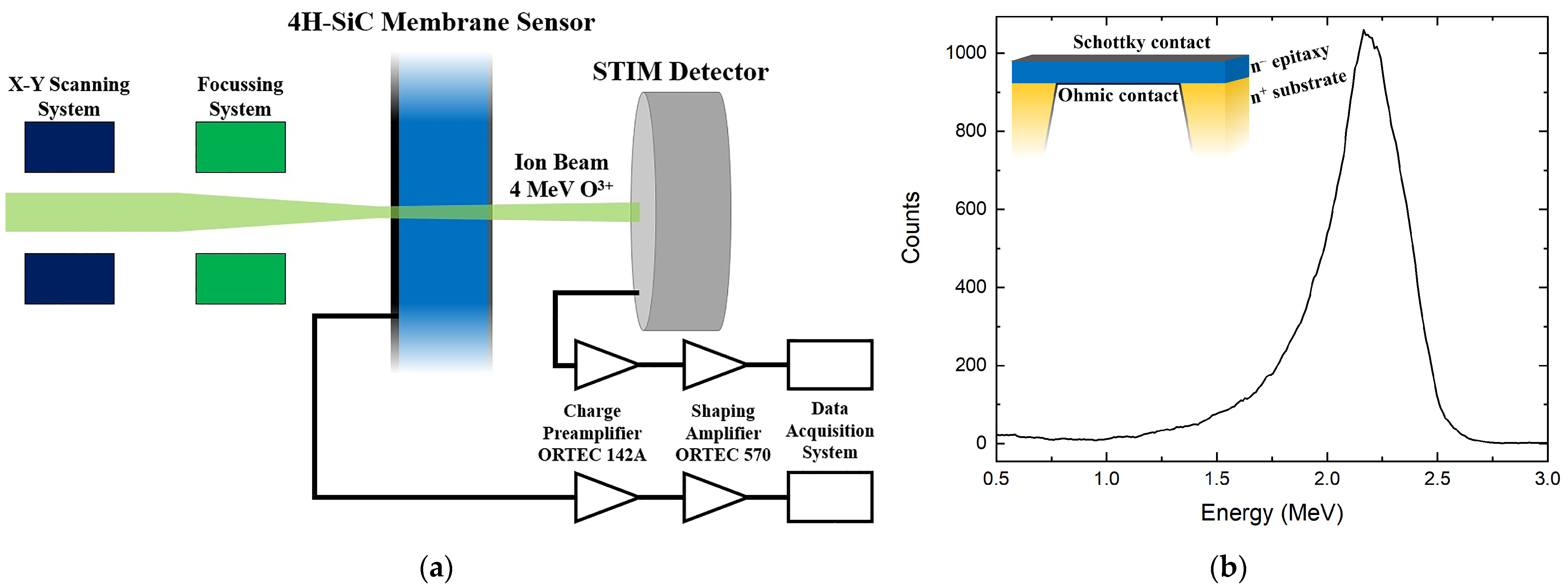
2. Materials and Methods
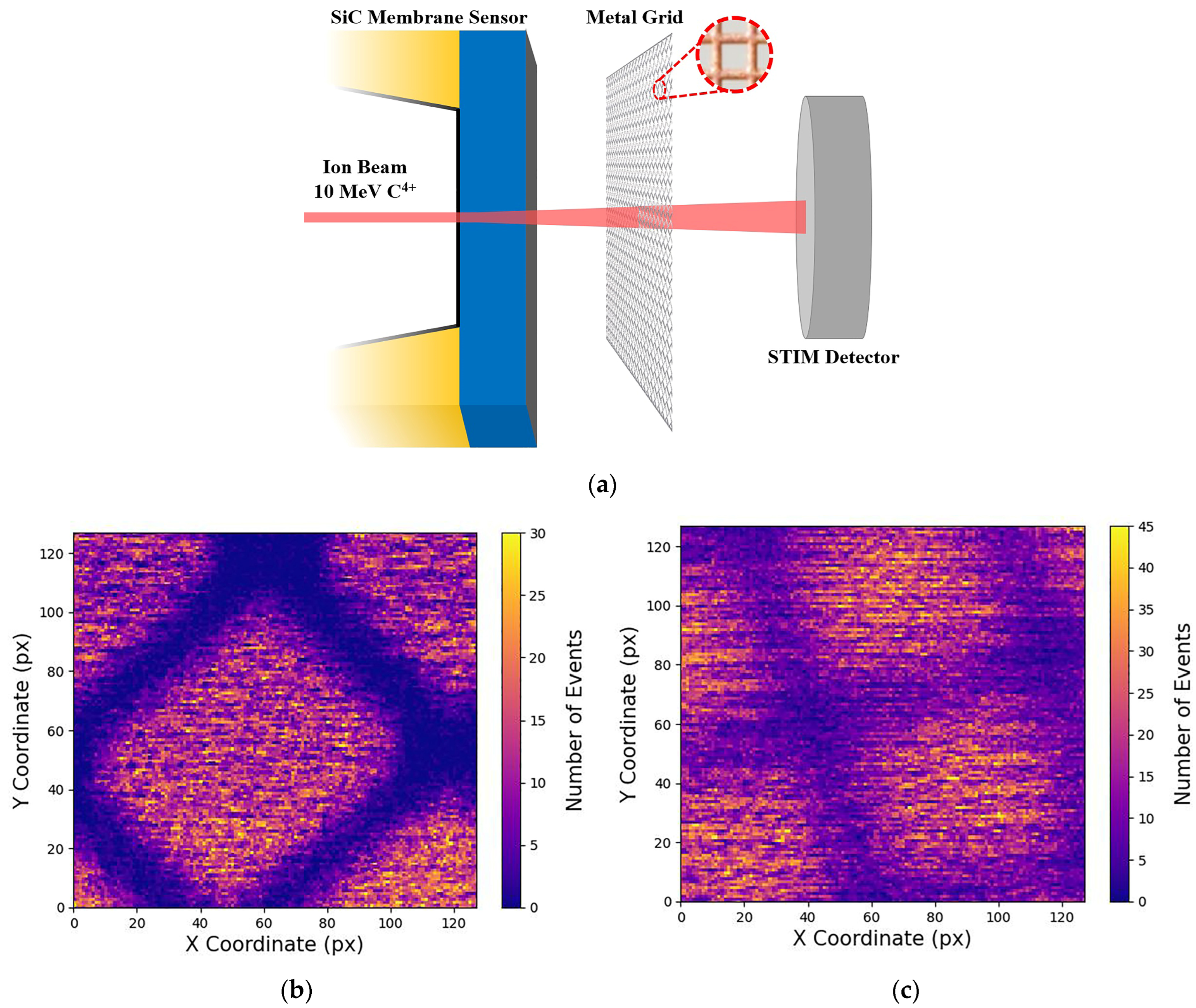
3. Results
3.1. Counting Measurement
3.2. Lateral Straggling
4. Discussion
5. Conclusions
Author Contributions
Funding
Data Availability Statement
Acknowledgments
Conflicts of Interest
References
- Kane, B.E. A silicon-based nuclear spin quantum computer. Nature 1998, 393, 133–137. [Google Scholar] [CrossRef]
- Hollenberg, L.C.L.; Dzurak, A.S.; Wellard, C.; Hamilton, A.R.; Reilly, D.J.; Milburn, G.J.; Clark, R.G. Charge-based quantum computing using single donors in semiconductors. Phys. Rev. B 2004, 69, 113301. [Google Scholar] [CrossRef]
- Morello, A.; Pla, J.J.; Zwanenburg, F.A.; Chan, K.W.; Tan, K.Y.; Huebl, H.; Möttönen, M.; Nugroho, C.D.; Yang, C.; van Donkelaar, J.A.; et al. Single-shot readout of an electron spin in silicon. Nature 2010, 467, 687–691. [Google Scholar] [CrossRef] [PubMed]
- Tyryshkin, A.M.; Lyon, S.A.; Astashkin, A.V.; Raitsimring, A.M. Electron spin relaxation times of phosphorus donors in silicon. Phys. Rev. B 2003, 68, 193207. [Google Scholar] [CrossRef]
- Kalra, R.; Laucht, A.; Hill, C.D.; Morello, A. Robust Two-Qubit Gates for Donors in Silicon Controlled by Hyperfine Interactions. Phys. Rev. X 2014, 4, 021044. [Google Scholar] [CrossRef]
- Pla, J.J.; Tan, K.Y.; Dehollain, J.P.; Lim, W.H.; Morton, J.J.L.; Zwanenburg, F.A.; Jamieson, D.N.; Dzurak, A.S.; Morello, A. High-fidelity readout and control of a nuclear spin qubit in silicon. Nature 2013, 496, 334–338. [Google Scholar] [CrossRef] [PubMed]
- Shields, B.J.; Unterreithmeier, Q.P.; de Leon, N.P.; Park, H.; Lukin, M.D. Efficient Readout of a Single Spin State in Diamond via Spin-to-Charge Conversion. Phys. Rev. Lett. 2015, 114, 136402. [Google Scholar] [CrossRef] [PubMed]
- Englund, D.; Shields, B.; Rivoire, K.; Hatami, F.; Vučković, J.; Park, H.; Lukin, M.D. Deterministic Coupling of a Single Nitrogen Vacancy Center to a Photonic Crystal Cavity. Nano Lett. 2010, 10, 3922–3926. [Google Scholar] [CrossRef]
- van Donkelaar, J.; Yang, C.; Alves, A.D.C.; McCallum, J.C.; Hougaard, C.; Johnson, B.C.; Hudson, F.E.; Dzurak, A.S.; Morello, A.; Spemann, D.; et al. Single atom devices by ion implantation. J. Phys. Condens. Matter 2015, 27, 154204. [Google Scholar] [CrossRef]
- Rueß, F.J.; Pok, W.; Reusch, T.C.G.; Butcher, M.J.; Goh, K.E.J.; Oberbeck, L.; Scappucci, G.; Hamilton, A.R.; Simmons, M.Y. Realization of Atomically Controlled Dopant Devices in Silicon. Small 2007, 3, 563–567. [Google Scholar] [CrossRef]
- Fuechsle, M.; Miwa, J.A.; Mahapatra, S.; Ryu, H.; Lee, S.; Warschkow, O.; Hollenberg, L.C.L.; Klimeck, G.; Simmons, M.Y. A single-atom transistor. Nat. Nanotechnol. 2012, 7, 242–246. [Google Scholar] [CrossRef] [PubMed]
- Stock, T.J.Z.; Warschkow, O.; Constantinou, P.C.; Li, J.; Fearn, S.; Crane, E.; Hofmann, E.V.S.; Kölker, A.; McKenzie, D.R.; Schofield, S.R.; et al. Atomic-Scale Patterning of Arsenic in Silicon by Scanning Tunneling Microscopy. ACS Nano 2020, 14, 3316–3327. [Google Scholar] [CrossRef] [PubMed]
- Koenraad, P.M.; Flatté, M.E. Single dopants in semiconductors. Nat. Mater. 2011, 10, 91–100. [Google Scholar] [CrossRef] [PubMed]
- Yang, C.; Jamieson, D.N.; Pakes, C.; Prawer, S.; Dzurak, A.; Stanley, F.; Spizziri, P.; Macks, L.; Gauja, E.; Clark, R.G. Single Phosphorus Ion Implantation into Prefabricated Nanometre Cells of Silicon Devices for Quantum Bit Fabrication. Jpn. J. Appl. Phys. 2003, 42, 4124–4128. [Google Scholar] [CrossRef]
- Shinada, T.; Okamoto, S.; Kobayashi, T.; Ohdomari, I. Enhancing semiconductor device performance using ordered dopant arrays. Nature 2005, 437, 1128–1131. [Google Scholar] [CrossRef] [PubMed]
- Schenkel, T.; Persaud, A.; Park, S.J.; Nilsson, J.; Bokor, J.; Liddle, J.A.; Keller, R.; Schneider, D.H.; Cheng, D.W.; Humphries, D.E. Solid state quantum computer development in silicon with single ion implantation. J. Appl. Phys. 2003, 94, 7017–7024. [Google Scholar] [CrossRef]
- Jamieson, D.N.; Yang, C.; Hopf, T.; Hearne, S.M.; Pakes, C.I.; Prawer, S.; Mitic, M.; Gauja, E.; Andresen, S.E.; Hudson, F.E.; et al. Controlled shallow single-ion implantation in silicon using an active substrate for sub-20-keV ions. Appl. Phys. Lett. 2005, 86, 202101. [Google Scholar] [CrossRef]
- Johnson, B.C.; Tettamanzi, G.; Yang, C.; Alves, A.; Van Donkelaar, J.; Thompson, S.; Verduijn, A.; Mol, J.A.; Wacquez, R.; Vinet, M.; et al. Single Ion Implantation into Si-Based Devices. ECS Trans. 2010, 33, 179–189. [Google Scholar] [CrossRef]
- Batra, A.; Weis, C.D.; Reijonen, J.; Persaud, A.; Schenkel, T.; Cabrini, S.; Lo, C.C.; Bokor, J. Detection of low energy single ion impacts in micron scale transistors at room temperature. Appl. Phys. Lett. 2007, 91, 193502. [Google Scholar] [CrossRef]
- Nida, S.; Tsibizov, A.; Ziemann, T.; Woerle, J.; Moesch, A.; Schulze-Briese, C.; Pradervand, C.; Tudisco, S.; Sigg, H.; Bunk, O.; et al. Silicon carbide X-ray beam position monitors for synchrotron applications. J. Synchrotron Radiat. 2019, 26, 28–35. [Google Scholar] [CrossRef]
- Mokhtarzadeh, M.; Carulla, M.; Kozak, R.; David, C. Optimization of etching processes for the fabrication of smooth silicon carbide membranes for applications in quantum technology. Micro Nano Eng. 2022, 16, 100155. [Google Scholar] [CrossRef]
- Gautier, G.; Defforge, T.; Gommé, G.; Valente, D.; Alquier, D. Electrochemical Formation of Porous Silicon Carbide for Micro-Device Applications. Mater. Sci. Forum 2018, 924, 943–946. [Google Scholar] [CrossRef]
- Accelerators—Ruđer Bošković Institute. Available online: https://www.irb.hr/eng/Divisions/Division-of-Experimental-Physics/Laboratory-for-ion-beam-interactions/Articles/Accelerators (accessed on 20 October 2023).
- Breese, M.; Vittone, E.; Vizkelethy, G.; Sellin, P. A review of ion beam induced charge microscopy. Nucl. Instrum. Methods Phys. Res. B 2007, 264, 345–360. [Google Scholar] [CrossRef]
- Breese, M.B.H.; Jamieson, D.N.; King, P.J.C. Materials Analysis Using a Nuclear Microprobe; John Wiley: Hoboken, NJ, USA, 1996; ISBN 0471106089. [Google Scholar]
- James Ziegler—SRIM & TRIM. Available online: http://www.srim.org/ (accessed on 20 October 2023).
- Cosic, D.; Bogovac, M.; Jakšić, M. Data acquisition and control system for an evolving nuclear microprobe. Nucl. Instrum. Methods Phys. Res. Sect. B Beam Interact. Mater. Atoms 2019, 451, 122–126. [Google Scholar] [CrossRef]
- Nguyen, T.-K.; Phan, H.-P.; Kamble, H.; Vadivelu, R.; Dinh, T.; Iacopi, A.; Walker, G.; Hold, L.; Nguyen, N.-T.; Dao, D.V. Superior Robust Ultrathin Single-Crystalline Silicon Carbide Membrane as a Versatile Platform for Biological Applications. ACS Appl. Mater. Interfaces 2017, 9, 41641–41647. [Google Scholar] [CrossRef]


Disclaimer/Publisher’s Note: The statements, opinions and data contained in all publications are solely those of the individual author(s) and contributor(s) and not of MDPI and/or the editor(s). MDPI and/or the editor(s) disclaim responsibility for any injury to people or property resulting from any ideas, methods, instructions or products referred to in the content. |
© 2023 by the authors. Licensee MDPI, Basel, Switzerland. This article is an open access article distributed under the terms and conditions of the Creative Commons Attribution (CC BY) license (https://creativecommons.org/licenses/by/4.0/).
Share and Cite
Sangregorio, E.; Calcagno, L.; Medina, E.; Crnjac, A.; Jakšic, M.; Vignati, A.; Romano, F.; Milluzzo, G.; De Napoli, M.; Camarda, M. Single-Ion Counting with an Ultra-Thin-Membrane Silicon Carbide Sensor. Materials 2023, 16, 7692. https://doi.org/10.3390/ma16247692
Sangregorio E, Calcagno L, Medina E, Crnjac A, Jakšic M, Vignati A, Romano F, Milluzzo G, De Napoli M, Camarda M. Single-Ion Counting with an Ultra-Thin-Membrane Silicon Carbide Sensor. Materials. 2023; 16(24):7692. https://doi.org/10.3390/ma16247692
Chicago/Turabian StyleSangregorio, Enrico, Lucia Calcagno, Elisabetta Medina, Andreo Crnjac, Milko Jakšic, Anna Vignati, Francesco Romano, Giuliana Milluzzo, Marzio De Napoli, and Massimo Camarda. 2023. "Single-Ion Counting with an Ultra-Thin-Membrane Silicon Carbide Sensor" Materials 16, no. 24: 7692. https://doi.org/10.3390/ma16247692
APA StyleSangregorio, E., Calcagno, L., Medina, E., Crnjac, A., Jakšic, M., Vignati, A., Romano, F., Milluzzo, G., De Napoli, M., & Camarda, M. (2023). Single-Ion Counting with an Ultra-Thin-Membrane Silicon Carbide Sensor. Materials, 16(24), 7692. https://doi.org/10.3390/ma16247692