

Laser Powder Bed Fusion of Molybdenum and Mo-0.1SiC Studied by Positron Annihilation Lifetime Spectroscopy and Electron Backscatter Diffraction Methods †

 , , , ,
Abstract
:1. Introduction
2. Materials and Methods
2.1. Specimen Preparation
2.2. Electron Backscatter Diffraction Preparation
2.3. Positron Measurements
3. Results
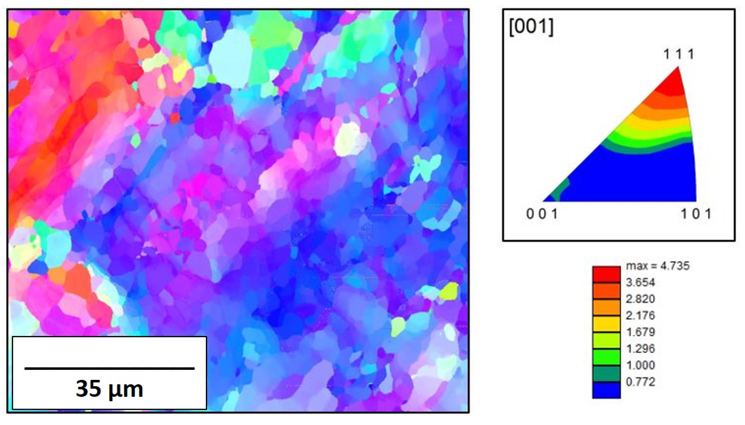
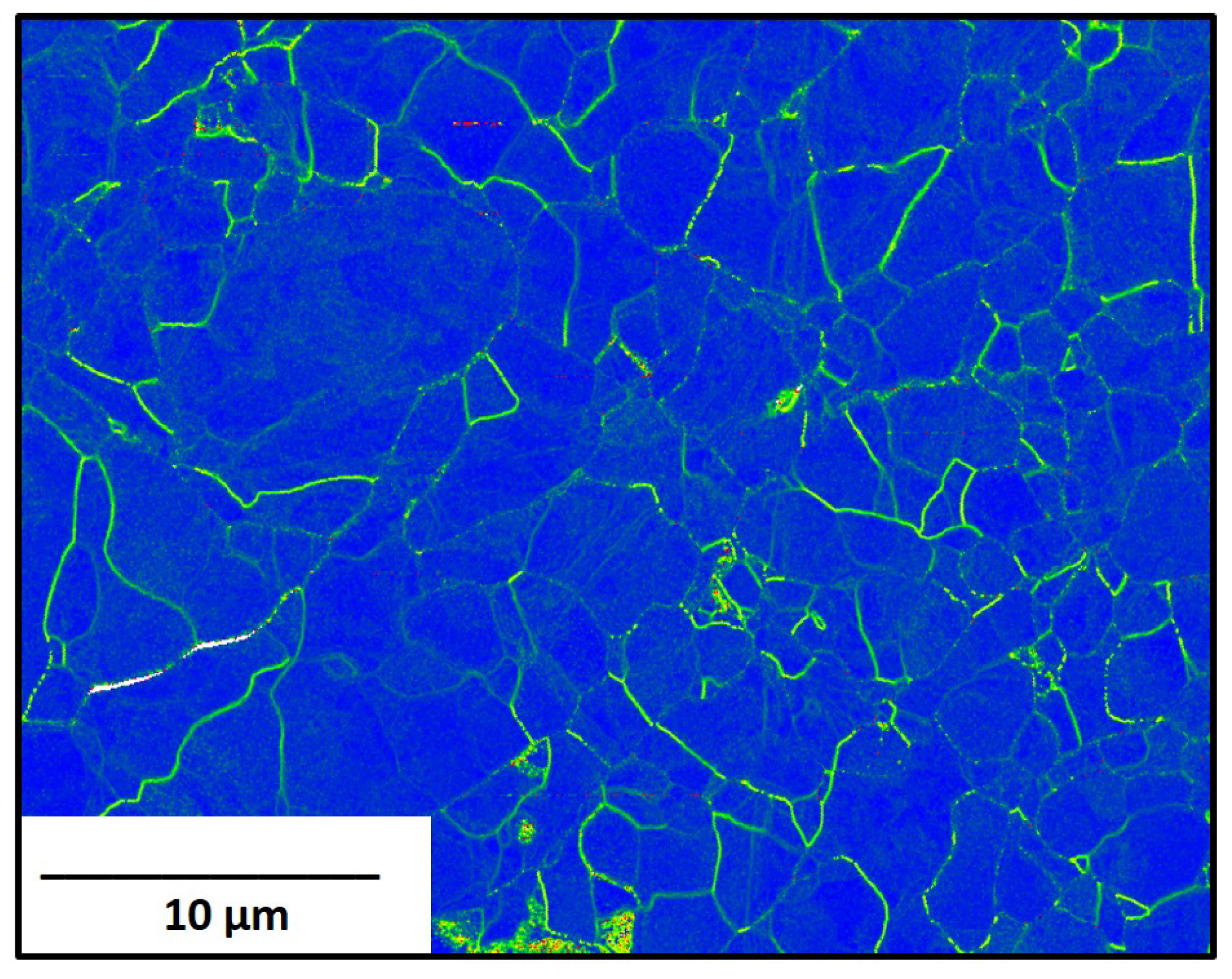
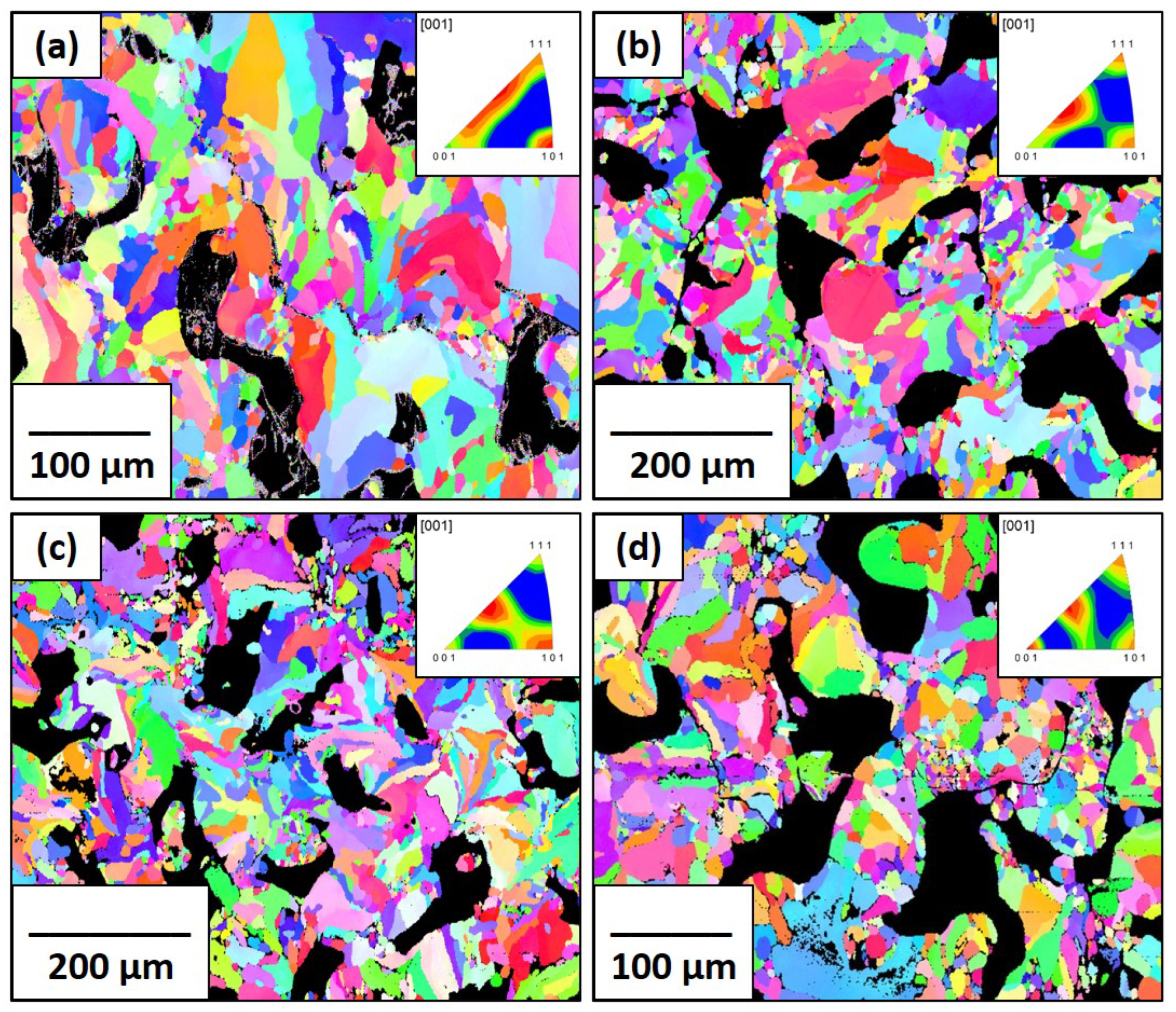
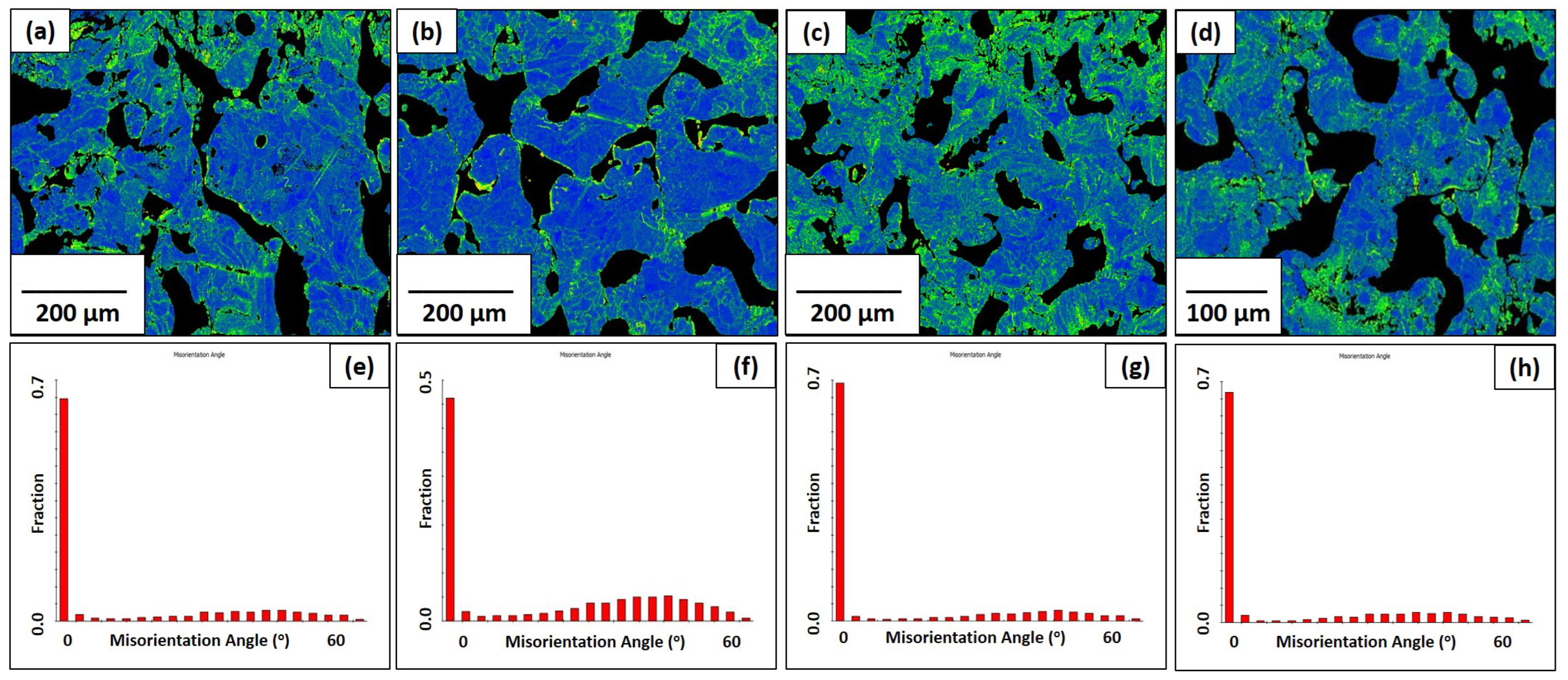
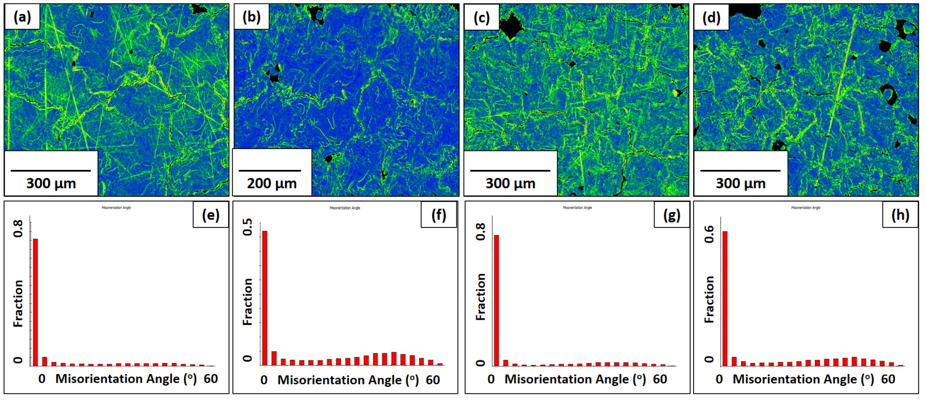
3.1. EBSD Analysis
3.2. Positron Lifetime Measurements
4. Discussion
4.1. Grain Boundaries
4.2. Defect-Free Bulk Material
4.3. Dislocations
4.4. Secondary Phases
4.5. Voids
5. Conclusions
- 1.
- Grain boundary evolution during the LPBF process was observable through IPF plots and KAM maps; however, their influence on the positron annihilation characteristics was insignificant, indicating the positrons were sampling sub-grain nano-scale features.
- 2.
- PALS measurements highlight the presence of silicon oxide nanoparticles and the greatly increased dislocation density in the Mo-0.1SiC, a microstructural feature that was not readily observable from the EBSD analysis.
- 3.
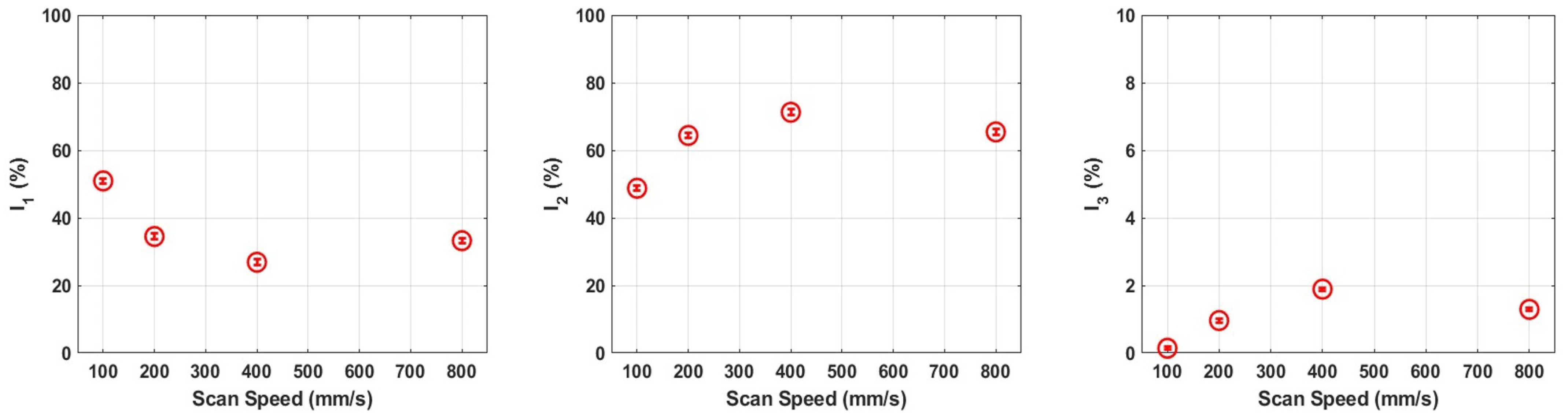
- PALS provides evidence that the quantity of silicon oxide nanoparticles in the consolidated material increases at higher laser scan speeds, information that was similarly unobtainable from other analyses.
- 4.
- Nano-voids are present in the Mo-0.1SiC specimens as a result of metal vaporization; however, the subsurface, bulk nature of these pores does not easily allow for non-destructive analysis through traditional electron microscopy techniques.
Author Contributions
Funding
Institutional Review Board Statement
Informed Consent Statement
Data Availability Statement
Conflicts of Interest
References
- Mackenzie, I.K.; Khoo, T.L.; McDonald, A.B.; Mckee, B.T. Temperature dependence of positron mean lives in metals. Phys. Rev. Lett. 1967, 19, 946–948. [Google Scholar] [CrossRef]
- Dryzek, J.; Wróbel, M. Detection of dynamical recrystallization in a tribolayer or pure molybdenum using positron annihilation and EBSD techniques. Wear 2021, 466–467, 203524. [Google Scholar] [CrossRef]
- Dryzek, J.; Wróbel, M. Recovery and recrystallization in molybdenum studied by positron annihilation and X-ray methods. Int. J. Refract. Met. Hard Mater. 2021, 97, 105514. [Google Scholar] [CrossRef]
- Dryzek, J.; Wróbel, M. Studies of recrystallization in rhenium using positron annihilation spectroscopy. Scr. Mater. 2022, 221, 114972. [Google Scholar] [CrossRef]
- Dryzek, J.; Wróbel, M.; Czeppe, T. Recovery and recrystallization in vanadium foil studied by positron annihilation and X-ray methods. Int. J. Refract. Met. Hard Mater. 2022, 103, 105759. [Google Scholar] [CrossRef]
- Dryzek, J.; Wróbel, M. Detection of tribolayer in pure iron using positron annihilation and EBSD techniques. Tribol. Int. 2020, 144, 106133. [Google Scholar] [CrossRef]
- Dryzek, J.; Wróbel, M. Evolution and thermal stability of the subsurface zone in copper formed in dry and lubricated sliding tests studied by positron annihilation and EBSD techniques. Wear 2021, 15, 204077. [Google Scholar] [CrossRef]
- Kemnitz, R.; Eckley, C.; Sexton, B.; LeSieur, A. Strengthening of additively manufactured tungsten by use of hydrogen in argon shielding gas. Int. J. Refract. Met. Hard Mater. 2023, 110, 105970. [Google Scholar] [CrossRef]
- Yan, A.; Atif, A.M.; Wang, X.; Lan, T.; Wang, Z. The microstructure and cracking behaviors of pure molybdenum fabricated by selective laser melting. Materials 2022, 15, 6230. [Google Scholar] [CrossRef]
- Eckley, C.; Kemnitz, R.; Fassio, C.; Hartsfield, C.; Leonhardt, T. Selective laser melting of tungsten-rhenium alloys. JOM 2021, 74, 3439–3450. [Google Scholar] [CrossRef]
- Forien, J.-B.; Calta, N.P.; DePond, P.J.; Guss, G.M.; Roehling, T.T.; Matthews, M.J. Detecting keyhole pore defects and monitoring process signatures during laser powder bed fusion: A correlation between in-situ pyrometry and ex-situ X-ray radiography. Addit. Manuf. 2020, 35, 101336. [Google Scholar] [CrossRef]
- Charalampous, P.; Kostavelis, I.; Tzovaras, D. Non-destructive quality control methods in additive manufacturing: A survey. Rapid Prototyp. J. 2020, 26, 777–790. [Google Scholar] [CrossRef]
- Berumen, S.; Bechmann, F.; Lindner, S.; Kruth, J.P.; Craeghs, T. Quality control of laser- and powder bed-based additive manufacturing (AM) techniques. Phys. Procedia 2010, 5, 617–622. [Google Scholar] [CrossRef] [Green Version]
- Zhao, C.; Fezzaa, K.; Cunningham, R.A.W.; Wen, H.; De Carlo, F.; Chen, L.; Rollett, A.D.; Sun, T. Real-time monitoring of laser powder bed fusion process using high-speed X-ray imaging and diffraction. Sci. Rep. 2017, 7, 1–11. [Google Scholar] [CrossRef]
- Hou, J.; You, Y.-W.; Kong, X.-S.; Song, J.; Liu, C.S. Accurate prediction of vacancy cluster structures and energetics in bcc transition metals. Acta Mater. 2021, 211, 116860. [Google Scholar] [CrossRef]
- Ruestes, C.J.; Bringa, E.M.; Stukowsi, A.; Rodriguez Nieva, J.F.; Tang, Y.; Meyers, M.A. Plastic deformation of a porous bcc metal containing nanometer sized voids. Comput. Mater. Sci. 2014, 88, 92–102. [Google Scholar] [CrossRef]
- Heikinheimo, J.; Mizohata, K.; Räisänen, J. Direct observation of mono-vacancy and self-interstitial recovery in tungsten. APL Mater. 2019, 7, 021103. [Google Scholar] [CrossRef] [Green Version]
- Keeble, D.J.; Brossman, U.; Puff, W.; Würschum, R. Positron Annihilation Studies of Materials. Charact. Mater. 2012. [Google Scholar] [CrossRef]
- Coleman, P. Positron Spectroscopy. In Digital Encyclopedia of Applied Physics; KGaA, Ed.; Wiley-VCH Verlag GmbH & Co.: Weinheim, Germany, 2009. [Google Scholar] [CrossRef]
- Wada, K.; Hyodo, T. A simple shape-free model for pore-size estimation with positron annihilation lifetime spectroscopy. J. Phys. Conf. Ser. 2013, 433, 012003. [Google Scholar] [CrossRef] [Green Version]
- Ellsworth, N.E.; Kemnitz, R.A.; Eckley, C.C.; Sexton, B.M.; Bowers, C.T.; Machacek, J.R.; Burggraf, L.W. Influence of Nano-Sized SiC on the Laser Powder Bed Fusion of Molybdenum. Crystals 2022, 12, 1276. [Google Scholar] [CrossRef]
- Hu, X.; Lach, T.G.; Terrani, K.A. Deuterium permeation and retention in 316L stainless steel manufactured by laser powder bed fusion. J. Nucl. Mater. 2021, 548, 152871. [Google Scholar] [CrossRef]
- Best, J.P.; Nomoto, K.; Yang, F.; Li, B.; Stolpe, M.; Zeng, L.; Evenson, Z.; Hugenschmidt, C.; Li, X.; Ringer, S.P.; et al. Advanced structural analysis of a laser additive manufactured Zr-based bulk metallic glass along the build height. J. Mater. Sci. 2022, 57, 9678–9692. [Google Scholar] [CrossRef]
- Eckert & Ziegler Reference & Calibration Sources: Product Information. Available online: https://www.ezag.com (accessed on 10 November 2022).
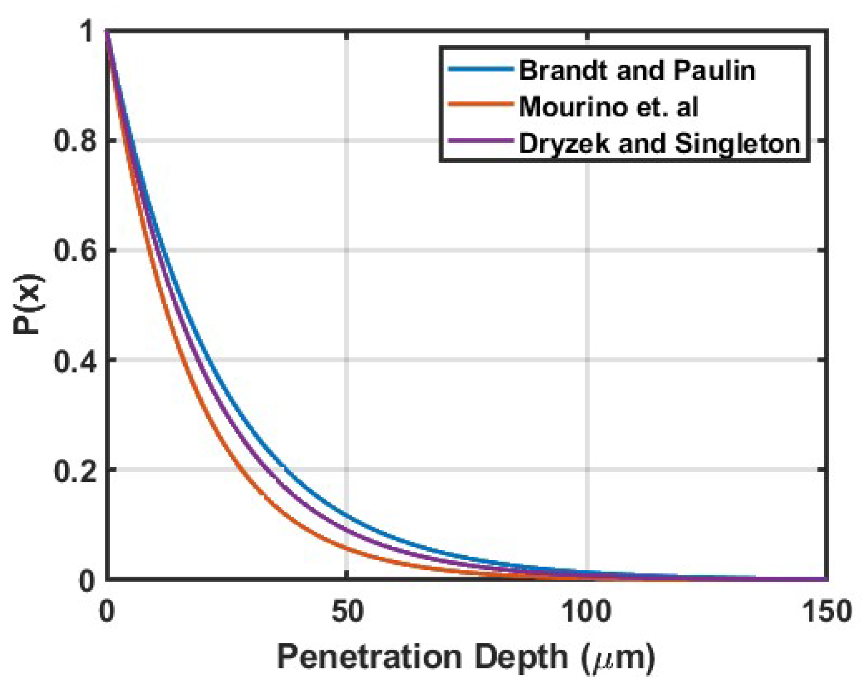
- Mourino, M.; Löbl, H.; Paulin, R. Profiles and absorption coefficients of positrons implanted in solids from radioactive sources. Phys. Lett. A 1979, 16, 106–108. [Google Scholar] [CrossRef]
- Brandt, W.; Paulin, R. Positron implantation-profile effects in solids. Phys. Rev. B 1977, 15, 2511–2518. [Google Scholar] [CrossRef]
- McGuire, S.; Keeble, D.J. Positron lifetimes of polycrystalline metals: A positron source correction study. J. Appl. Phys. 2006, 100, 103504. [Google Scholar] [CrossRef]
- Dryzek, J.; Singleton, D. Implantation profile and linear absorption coefficients for positrons injected in solids from radioactive sources 22Na and 68Ge/68Ga. Nucl. Instrum. Methods B 2006, 252, 197–204. [Google Scholar] [CrossRef]
- Campillo Robles, J.M.; Ogando, E.; Plazaola, F. Positron lifetime calculation for the elements of the periodic table. J. Phys. Condens. Matter 2007, 19, 176222. [Google Scholar] [CrossRef]
- Kirkegaard, P.; Olsen, J.; Eldrup, M. PALSfit3: A Software Package for Analysing Positron Lifetime Spectra; DTU Library: New Delhi, India, 2017. [Google Scholar]
- Siemek, K.; Horodek, P.; Skuratov, V.A.; Walizzewski, J.; Sohatsky, A. Positron annihilation studies of irradiation induced defects in nanostructured titanium. Vacuum 2021, 190, 110282. [Google Scholar] [CrossRef]
- McGuire, S.; Keeble, D.J. Positron lifetime and implantation in Kapton. J. Phys. D 2006, 39, 3388. [Google Scholar] [CrossRef]
- Bertolaccini, M.; Zappa, L. Source-supporting foil effect on the shape of positron time annihilation spectra. Il Nuovo Cimento B 1967, 52, 487–494. [Google Scholar] [CrossRef]
- Plotkowski, K.; Panek, T.J.; Kansy, J. Positron implantation profile in kapton. Il Nuovo Cimento D 1988, 10, 933–940. [Google Scholar] [CrossRef]
- Saoucha, A. Positron transmission into Kapton: The effective mass absorption coefficient of relevance to positron lifetime experiments. J. Appl. Phys. 1999, 85, 1802–1810. [Google Scholar] [CrossRef]
- Staab, T.E.M.; Somieski, B.; Krause-Rehberg, R. The data treatment influence on the spectra decomposition in positron lifetime spectroscopy Part 2: The effect of source corrections. Nucl. Instrum. Methods A 1996, 381, 141–151. [Google Scholar] [CrossRef]
- Bernardin, M.; Dupasquier, A.; Gallone, A.; Pizzi, P. Positron annihilation study of ageing and creep of Inconel X750. Phys. Stat. Sol. A 1979, 56, 277–284. [Google Scholar] [CrossRef]
- ASTM B387-18; Standard Specification for Molybdenum and Molybdenum Alloy Bar, Rod, Wire. American Society for Testing and Materials: West Conshohocken, PA, USA, 2018.
- Zhu, Z.; Chen, K.; Chen, J.; Xu, R.; Wang, Z. Positron lifetime study of proton-irradiated molybdenum. Nucl. Instrum. Methods B 1991, 61, 72–76. [Google Scholar]
- Pagh, B.; Hansen, H.E.; Nielsen, B.; Trumpy, G.; Petersen, K. Temperature dependence of positron annihilation parameters in neutron irradiated molybdenum. Appl. Phys. A 1984, 33, 255–263. [Google Scholar] [CrossRef]
- Staab, T.E.M.; Krause-Rehberg, R.; Kieback, B. Review: Positron annihilation in fine-grained materials and fine powders—An application to the sintering of metal powders. J. Mater. Sci. 1999, 34, 3833–3851. [Google Scholar] [CrossRef]
- Higashi, M.; Ozaki, T. Selective laser melting of pure molybdenum: Evolution of defect and crystallographic texture with process parameters. Mater. Des. 2020, 191, 108588. [Google Scholar] [CrossRef]
- Faraji, G.; Kim, H.S.; Kashi, H.T. (Eds.) Chapter 6: The Effective Parameters for the Success of Severe Plastic Deformation Methods. In Severe Plastic Deformation; Elsevier: Amsterdam, The Netherlands, 2018; pp. 187–222. [Google Scholar]
- Borodin, E.; Mayer, A.E. Influence of structure of grain boundaries and size distribution of grains on the yield strength at quasistatic and dynamical loading. Mater. Res. Express 2017, 4, 085040. [Google Scholar] [CrossRef]
- Ziegler, R.; Schaefer, H.E. Vacancy formation in molybdenum and tungsten investigated by positron lifetime measurements. Mater. Sci. Forum 1987, 15–18, 145–148. [Google Scholar] [CrossRef]
- Hyodo, T.; Mckee, B.T.A.; Stewart, A.T. Vacancy clusters in neutron irradiated molybdenum. Rad. Effects Lett. 1982, 68, 77–82. [Google Scholar] [CrossRef]
- Hautojärvi, P.; Heiniö, J.; Manninen, M.; Nieminen, R. The effect of microvoid size on positron annihilation characteristics and residual resistivity in metals. Philos. Mag. 1977, 35, 973–981. [Google Scholar] [CrossRef]
- Kuriplach, J.; Barbiellini, B. Improved generalized gradient approximation for positron states in solids. Phys. Rev. B 2014, 89, 155111. [Google Scholar] [CrossRef] [Green Version]
- Puska, M.J.; Mieminen, R.M. Theory of positrons in solids and on solid surface. Rev. Mod. Phys. 1994, 66, 841–897. [Google Scholar] [CrossRef] [Green Version]
- Suzuki, T.; Iida, S.; Yamashita, T.; Nahashima, Y. Measurement of positron diffusion constants in polycrystalline molybdenum by the observation of positronium negative ions. J. Phys. Conf. Ser. 2015, 618, 012015. [Google Scholar] [CrossRef]
- Arakawa, K.; Ono, K.; Isshiki, M.; Mimura, K.; Uchikoshi, M.; Mori, H. Observation of the one-dimensional diffusion of nanometer-sized dislocation loops. Science 2007, 318, 956–959. [Google Scholar] [CrossRef] [Green Version]
- Standard Die International: Molybdenum. Available online: https://www.standarddie.com/materials/molybdenum (accessed on 14 November 2022).
- Zhang, C.; Li, Z.; Ye, Y.; Yuan, Y.; Fang, D.; Wu, H.; Li, W. Interaction of nanoparticles and dislocations with Mg17Al12 precipitates in n-SiCp/AZ91D magnesium matrix nanocomposites. J. Alloys Cmpd. 2020, 815, 152416. [Google Scholar] [CrossRef]
- Abbas, M.A.; Anru, Y.; Wang, Z.Y. Comparative study of additively manufactured samples of tungsten with molybdenum and their applications. IOP Conf. Ser. Earth Environ. Sci. 2022, 968, 012008. [Google Scholar] [CrossRef]
- Liu, J.; Peng, W. Metal vaporization and its influence during laser powder bed fusion process. Mater. Des. 2022, 215, 110505. [Google Scholar] [CrossRef]
- Simnad, M.; Spilners, A. Kinetics and mechanism of the oxidation of molybdenum. JOM 1955, 7, 1011–1016. [Google Scholar] [CrossRef]
- Shrestha, S.; Starr, T.; Chou, K. A study of keyhole porosity in selective laser melting: Single-track scanning with micro-CT analysis. J. Manuf. Sci. Eng. 2019, 141, 071004. [Google Scholar] [CrossRef]


| (ps) | I1 (%) | (ps) | I2 (%) | (ps) | I3 (%) |
|---|---|---|---|---|---|
| 121.7 ± 1.2 | 77.15 ± 0.73 | 282.9 ± 5.1 | 20.77 ± 0.61 | 745.1 ± 20.8 | 2.08 ± 0.14 |
| Scan Speed | 100 (mm/s) | 200 (mm/s) | 400 (mm/s) | 800 (mm/s) |
|---|---|---|---|---|
| Molybdenum | 33.63 ± 4.34 | 27.63 ± 2.54 | 30.07 ± 3.10 | 22.91 ± 1.69 |
| Mo-0.1SiC | 47.94 ± 9.74 | 42.44 ± 5.89 | 26.32 ± 0.69 | 24.34 ± 1.05 |
| Scan Speed | 100 (mm/s) | 200 (mm/s) | 400 (mm/s) | 800 (mm/s) |
|---|---|---|---|---|
| Pure molybdenum | 0.33 ± 0.07 | 0.51 ± 0.03 | 0.45 ± 0.06 | 0.33 ± 0.03 |
| Mo-0.1SiC | 0.22 ± 0.04 | 0.44 ± 0.03 | 0.27 ± 0.08 | 0.40 ± 0.01 |
| Scan Speed (mm/s) | (ps) | (ps) | I1 (%) | I2 (%) | |
|---|---|---|---|---|---|
| 100 | 125.2 ± 0.1 | 751.5 ± 32.6 | 99.66 ± 0.02 | 0.34 ± 0.02 | 1.068 |
| 200 | 128.8 ± 0.2 | 534.1 ± 13.8 | 99.07 ± 0.04 | 0.93 ± 0.04 | 1.083 |
| 400 | 129.7 ± 0.2 | 414.8 ± 8.30 | 98.02 ± 0.09 | 1.97 ± 0.09 | 1.052 |
| 800 | 128.7 ± 0.2 | 464.4 ± 11.1 | 98.69 ± 0.07 | 1.31 ± 0.07 | 1.000 |
| Scan Speed (mm/s) | (ps) | (ps) | I1 (%) | I2 (%) | |
|---|---|---|---|---|---|
| 100 | 135.2 ± 0.3 | 415.0 ± 2.7 | 92.47 ± 0.12 | 7.53 ± 0.12 | 1.114 |
| 200 | 136.8 ± 0.3 | 384.8 ± 4.1 | 94.66 ± 0.15 | 5.34 ± 0.15 | 1.112 |
| 400 | 138.2 ± 0.3 | 368.9 ± 5.6 | 95.87 ± 0.17 | 4.13 ± 0.17 | 1.043 |
| 800 | 141.2 ± 0.3 | 409.3 ± 7.3 | 97.22 ± 0.12 | 2.78 ± 0.12 | 1.069 |
| Trapping Site | Positron Lifetime (ps) | Reference |
|---|---|---|
| Single Crystal | 103 | Ziegler and Schaefer [45] |
| Bulk | 115 | Hyodo et al. [46] |
| Dislocations | 135 | Dryzek and Wróbel [2,3] |
| Monovacancy | 170 | Robles et al. [29] |
| Divacancy | ∼249 | Dryzek and Wróbel, Hautojärvi et al. [3,47] |
| SiO2 | ∼261 | Kuriplach and Barbiellini [48] |
| Microvoids | 350–450 | Hautojärvi et al. [47] |
Disclaimer/Publisher’s Note: The statements, opinions and data contained in all publications are solely those of the individual author(s) and contributor(s) and not of MDPI and/or the editor(s). MDPI and/or the editor(s) disclaim responsibility for any injury to people or property resulting from any ideas, methods, instructions or products referred to in the content. |
© 2023 by the authors. Licensee MDPI, Basel, Switzerland. This article is an open access article distributed under the terms and conditions of the Creative Commons Attribution (CC BY) license (https://creativecommons.org/licenses/by/4.0/).
Share and Cite
Ellsworth, N.E.; Machacek, J.R.; Kemnitz, R.A.; Eckley, C.C.; Sexton, B.M.; Gearhart, J.A.; Burggraf, L.W. Laser Powder Bed Fusion of Molybdenum and Mo-0.1SiC Studied by Positron Annihilation Lifetime Spectroscopy and Electron Backscatter Diffraction Methods. Materials 2023, 16, 1636. https://doi.org/10.3390/ma16041636
Ellsworth NE, Machacek JR, Kemnitz RA, Eckley CC, Sexton BM, Gearhart JA, Burggraf LW. Laser Powder Bed Fusion of Molybdenum and Mo-0.1SiC Studied by Positron Annihilation Lifetime Spectroscopy and Electron Backscatter Diffraction Methods. Materials. 2023; 16(4):1636. https://doi.org/10.3390/ma16041636
Chicago/Turabian StyleEllsworth, Nathan E., Joshua R. Machacek, Ryan A. Kemnitz, Cayla C. Eckley, Brianna M. Sexton, Joel A. Gearhart, and Larry W. Burggraf. 2023. "Laser Powder Bed Fusion of Molybdenum and Mo-0.1SiC Studied by Positron Annihilation Lifetime Spectroscopy and Electron Backscatter Diffraction Methods" Materials 16, no. 4: 1636. https://doi.org/10.3390/ma16041636
APA StyleEllsworth, N. E., Machacek, J. R., Kemnitz, R. A., Eckley, C. C., Sexton, B. M., Gearhart, J. A., & Burggraf, L. W. (2023). Laser Powder Bed Fusion of Molybdenum and Mo-0.1SiC Studied by Positron Annihilation Lifetime Spectroscopy and Electron Backscatter Diffraction Methods. Materials, 16(4), 1636. https://doi.org/10.3390/ma16041636