
Study on Microstructure and Mechanical Properties at Constant Electromigration Temperature of Sn2.5Ag0.7Cu0.1RE0.05Ni-GNSs/Cu Solder Joints

Abstract
:1. Introduction
2. Experimental Materials and Methods
2.1. Materials
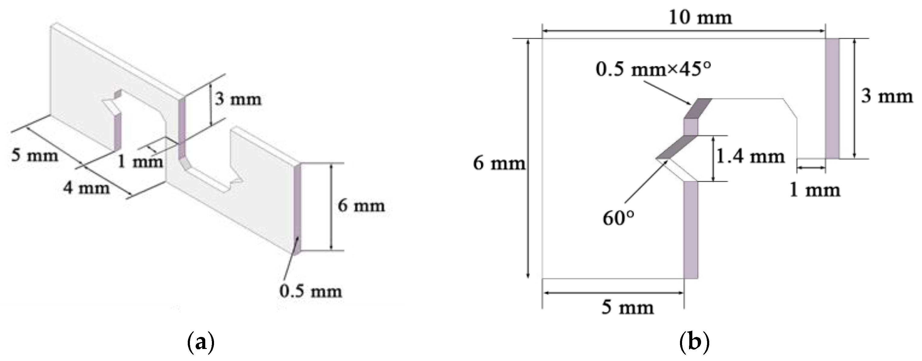
2.2. Soldering Test
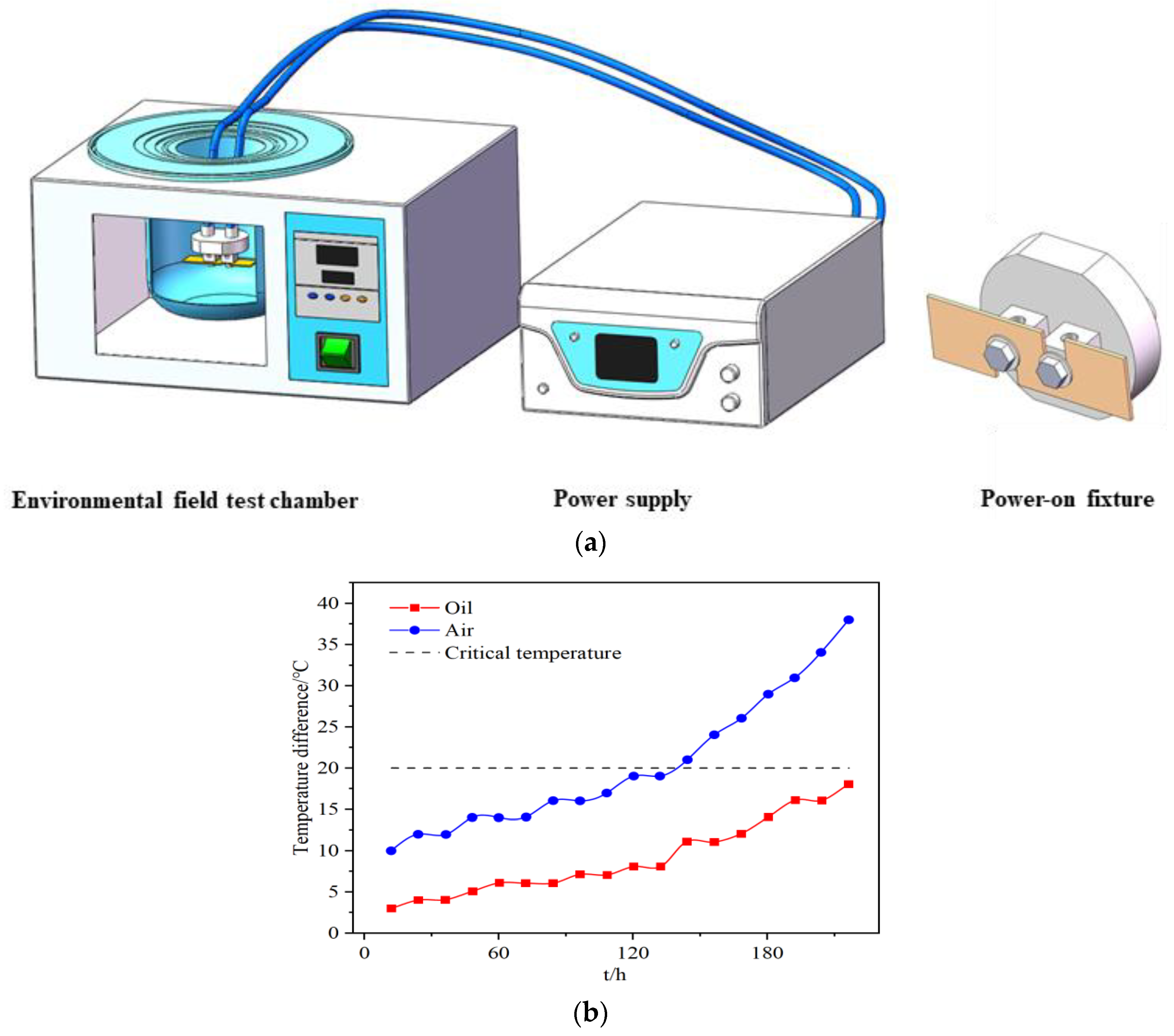
2.3. Electromigration Device Design, Manufacturing, and Testing
2.4. Test Scheme and Test Method
3. Results
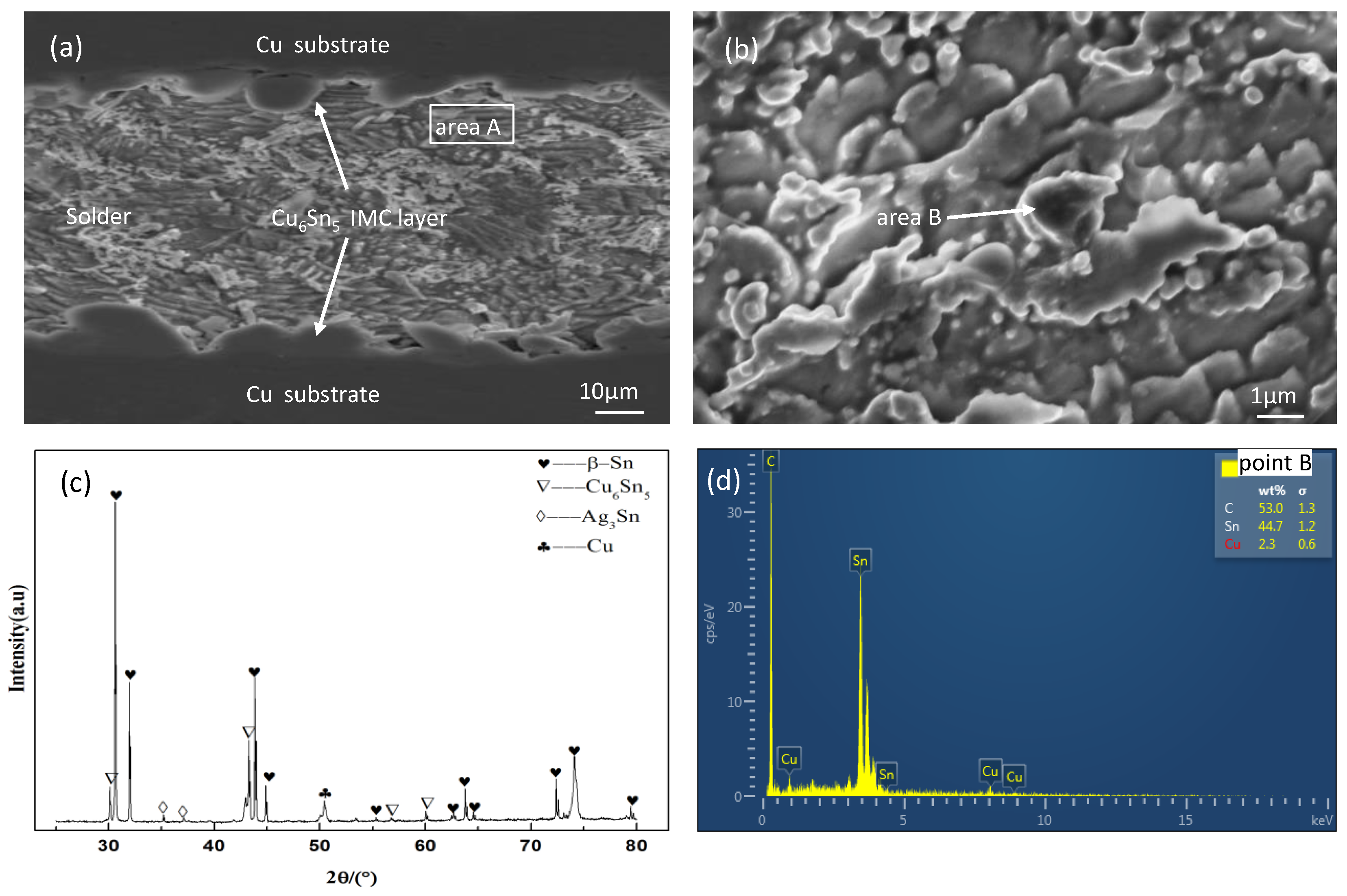
3.1. Microstructure of Solder Joints without Current Loading
3.2. Microstructure of Solder Joints during Current Loading
3.2.1. Impact of Current Density
3.2.2. Impact of the Current Loading Process
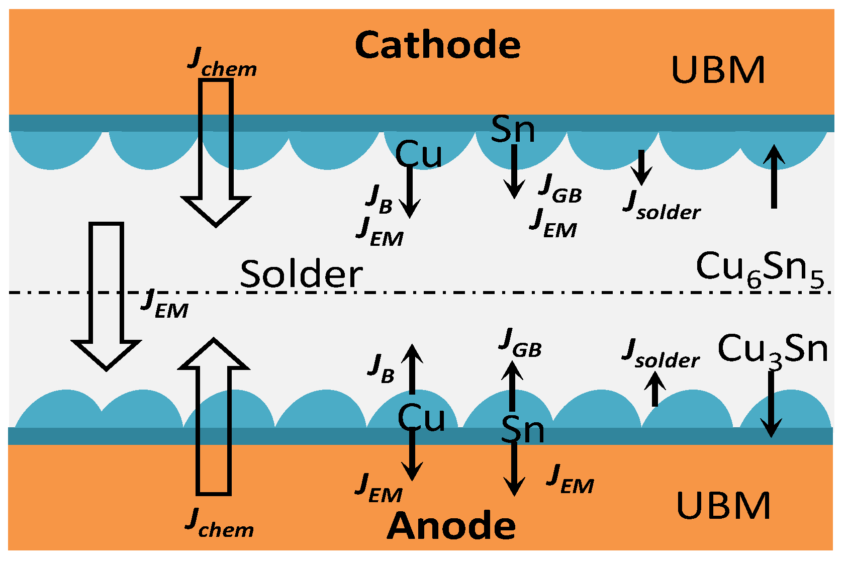
3.3. Interfacial Reaction Analysis in Electromigration of Solder Joints
3.4. Mechanical Properties and Fracture Mechanism of the Electromigration of Solder Joints
3.4.1. Electrical and Mechanical Properties
3.4.2. Mechanical Fracture Mechanism
4. Conclusions
- (1)
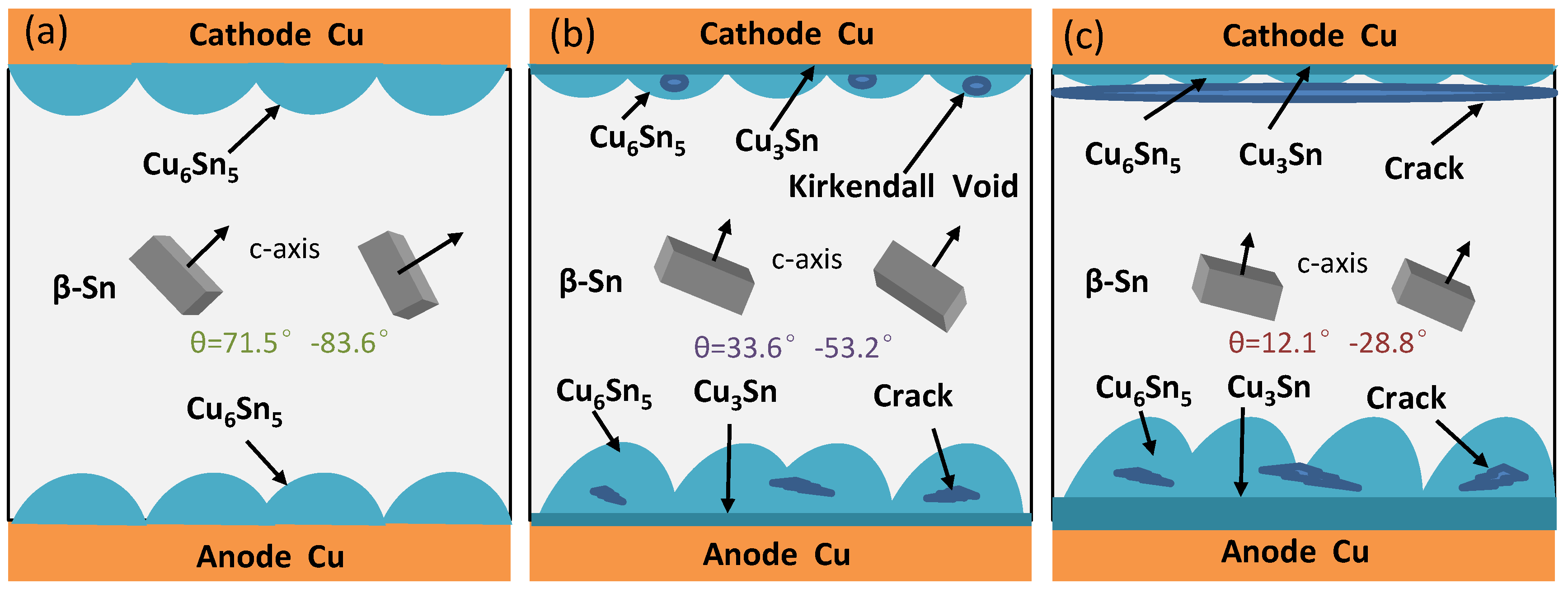
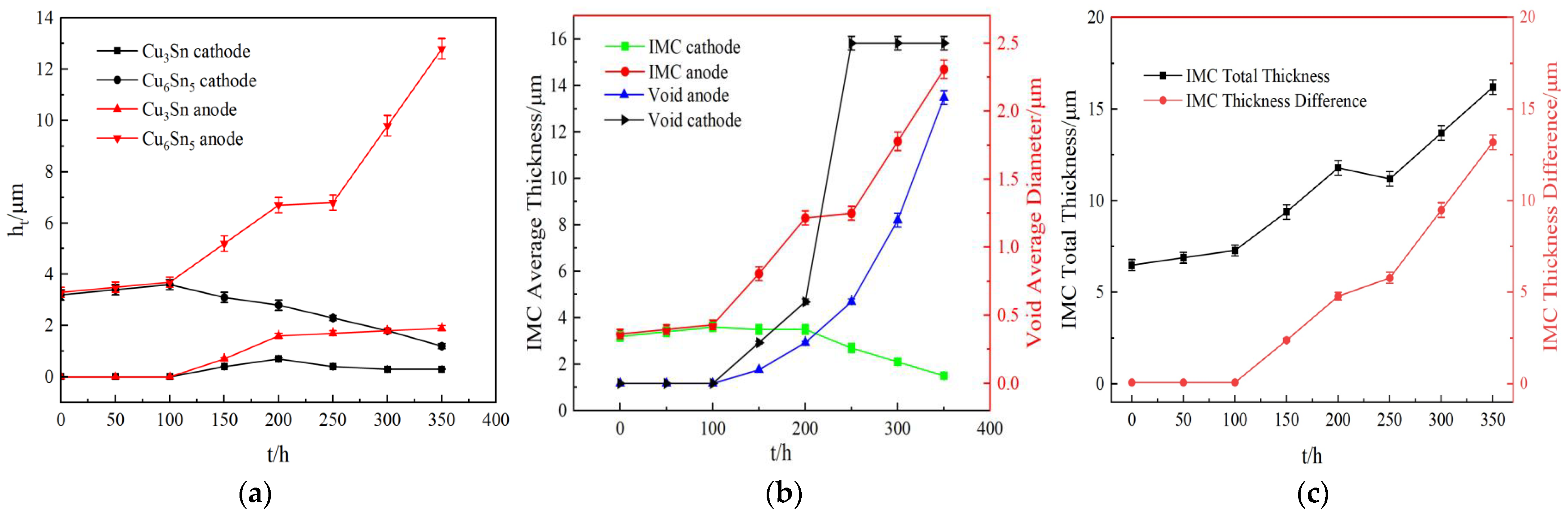
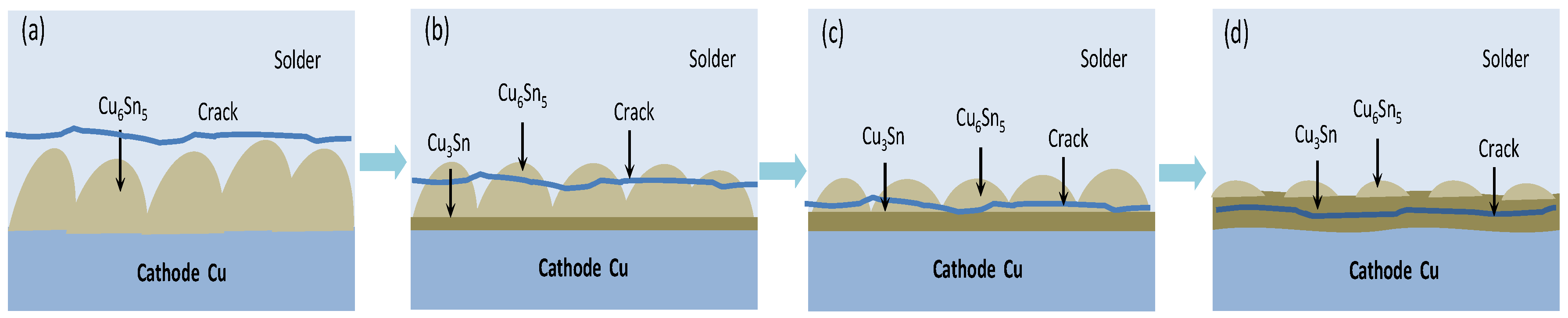
- With the ideal self−designed and manufactured electromigration device, Sn2.5Ag0.7Cu0.1RE0.05Ni−GNSs/Cu solder joints show evidence of typical electromigration polarity under the conditions of a typical electromigration polarity ≥ 7 × 10³ A/cm2 and included angle between the c−axis of the β−Sn grains and the current direction θ ≤ 53.2°. The anode−side interfacial IMC of the solder joints is dominated by a Cu6Sn5 phase, has a gradually increasing thickness, forms a Cu3Sn phase, and shows evidence of microcracks. The Cu6Sn5 phase of the cathode−side interfacial IMC is gradually completely dissolved, and the growth of the Cu3Sn phase is accompanied by the formation of Kirkendall voids.
- (2)
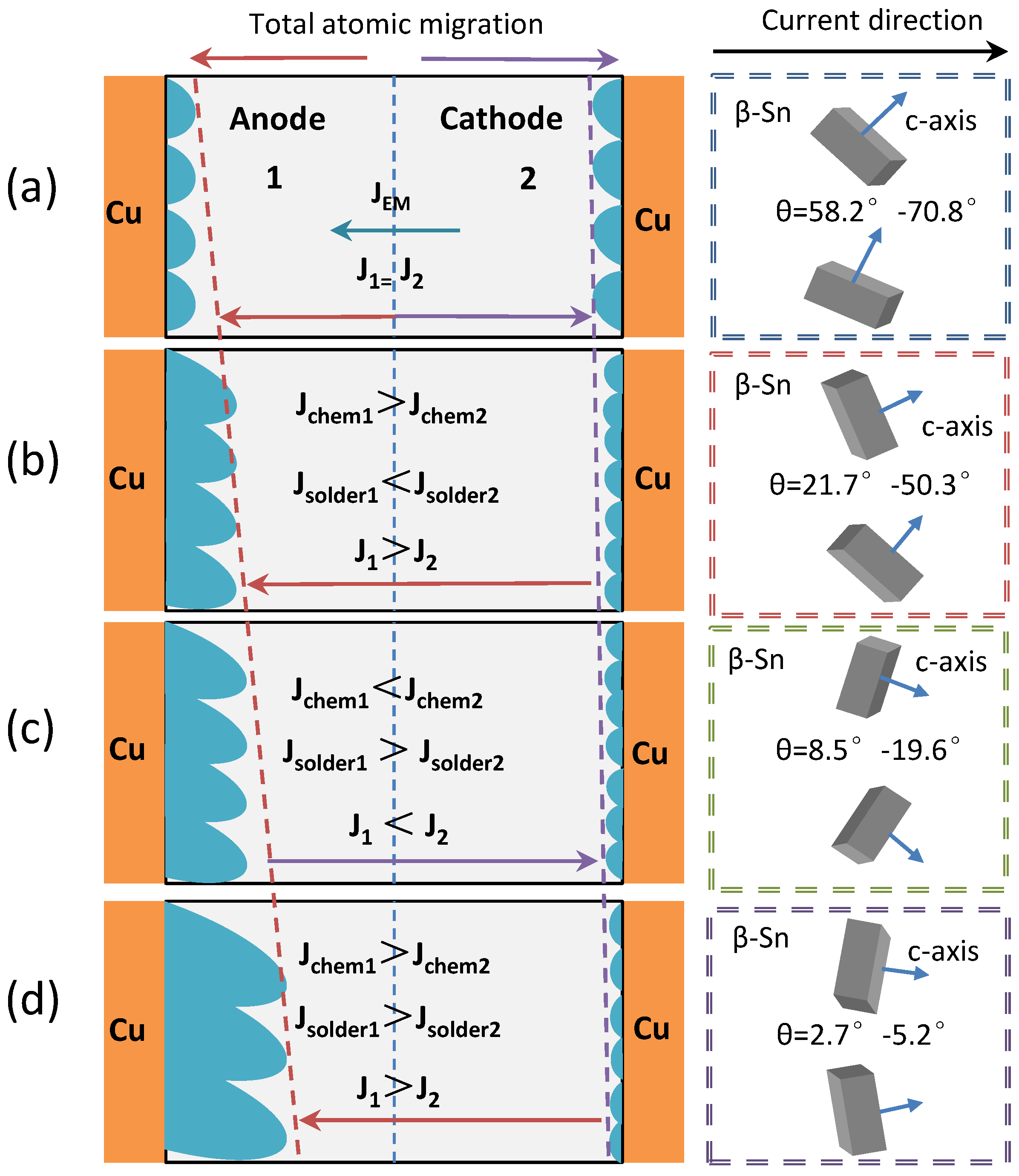
- The anisotropic diffusion of Cu atoms in β−Sn in the electromigration of Sn2.5Ag0.7Cu0.1RE0.05Ni−GNSs/Cu solder points affects four stages of electromigration: the incubation stage, expansion stage, stability stage, and failure stage. The process of electromigration can be decelerated through the reasonable adjustment and control of θ.
- (3)
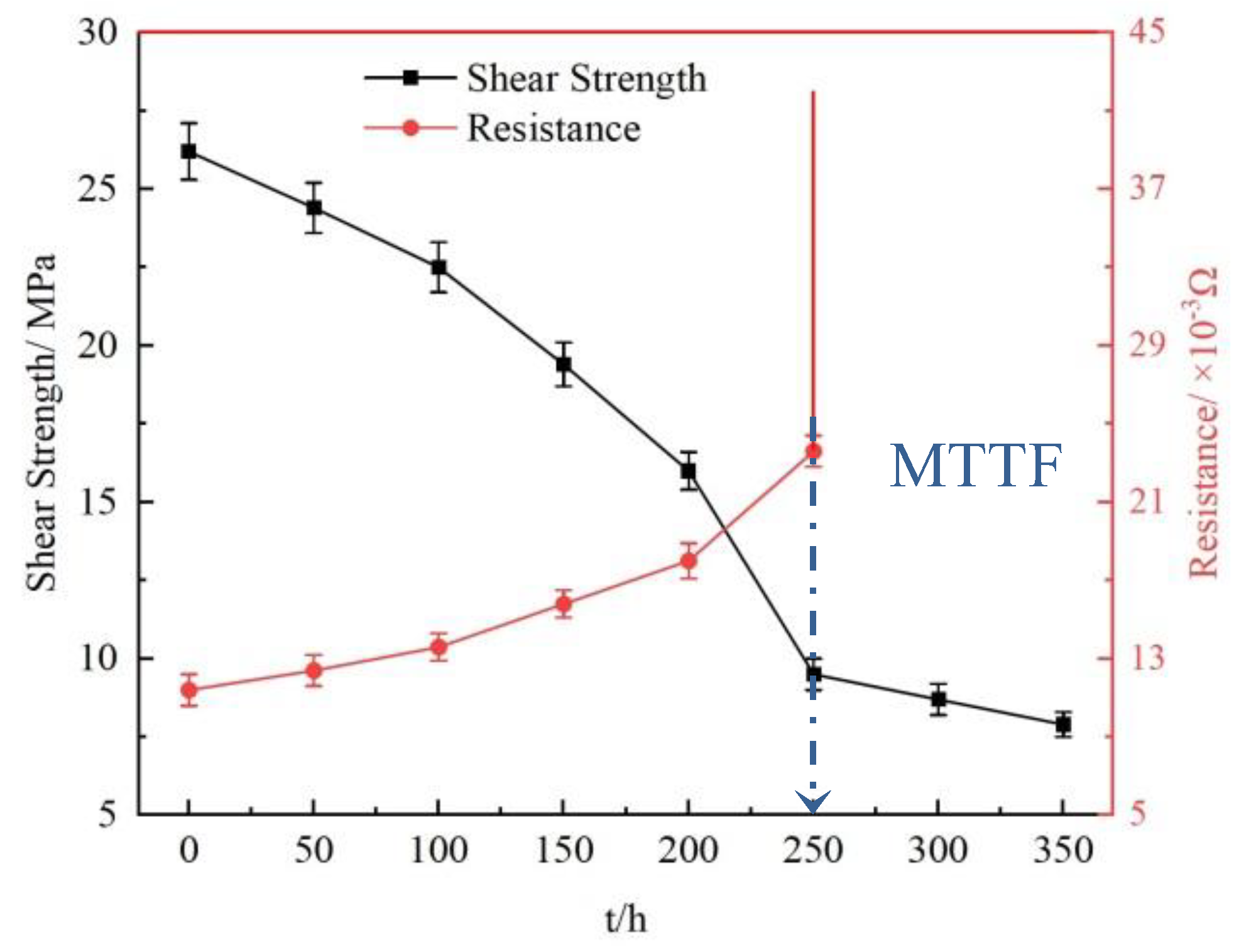
- In the four stages of electromigration of Sn2.5Ag0.7Cu0.1RE0.05Ni−GNSs/Cu solder joints, the increase in the resistance is inversely correlated with the decrease in the shear strength, and the solder joints reach the failure state at 250 h. The shear fracture path of the solder joints moves from the cathode side near the IMC solder seam to the Cu3Sn interface. The shear fracture mechanism changes from ductile transgranular fracture dominated by β−Sn dimples to brittle fracture dominated by interfacial IMC cleavage and slip steps.
Author Contributions
Funding
Institutional Review Board Statement
Informed Consent Statement
Data Availability Statement
Conflicts of Interest
References
- Li, Y.; Luo, K.M.; Lim, A.B.Y.; Chen, Z.; Wu, F.S.; Chan, Y.C. Improving the mechanical performance of Sn57.6Bi0.4Ag solder joints on Au/Ni/Cu pads during aging and electromigration through the addition of tungsten (W) nanoparticle reinforcement. Mater. Sci. Eng. A-Struct. Mater. Prop. Microstruct. Process. 2016, 669, 291–303. [Google Scholar] [CrossRef]
- Ahmed, M.T.; Motalab, M.; Suhling, J.C. Impact of Mechanical Property Degradation and Intermetallic Compound Formation on Electromigration-Oriented Failure of a Flip-Chip Solder Joint. J. Electron. Mater. 2021, 50, 233–248. [Google Scholar] [CrossRef]
- Peng, H.; Huang, B.M.; Chen, G.; Wul, F.S.; Liul, H.; Chan, Y.C. Effect of 0.8 wt% Al2O3 Nanoparticles Addition on the Microstructures and Electromigration Behavior of Sn-Ag-Cu Solder Joint. In Proceedings of the 16 International Conference Electronic Packaging Technology, Changsha, China, 11–14 August 2015; IEEE: Changsha, China, 2015. [Google Scholar]
- Fawzy, A.; Fayek, S.A.; Sobhy, M.; Nassr, E.; Mousa, M.M.; Saad, G. Tensile creep characteristics of Sn-3.5Ag-0.5Cu (SAC355) solder reinforced with nano-metric ZnO particles. Mater. Sci. Eng. A-Struct. Mater. Prop. Microstruct. Process. 2014, 603, 1–10. [Google Scholar] [CrossRef]
- Chiu, S.H.; Shao, T.L.; Chen, C.; Yao, D.J.; Hsu, C.Y. Infrared microscopy of hot spots induced by Joule heating in flip-chip SnAg solder joints under accelerated electromigration. Appl. Phys. Lett. 2006, 88, 5451. [Google Scholar] [CrossRef] [Green Version]
- Cheng, S.; Huang, C.M.; Pecht, M. A review of lead-free solders for electronics applications. Microelectron. Reliab. 2017, 75, 77–95. [Google Scholar] [CrossRef]
- Jiang, N.; Zhang, L.; Liu, Z.Q.; Sun, L.; Xu, K.K. Influences of doping Ti nanoparticles on microstructure and properties of Sn58Bi solder. J. Mater. Sci.: Mater. Electron. 2019, 30, 17583–17590. [Google Scholar] [CrossRef]
- Qu, M.; Cao, T.; Cui, Y.; Liu, F.; Jiao, Z. Effect of nano-ZnO particles on wettability, interfacial morphology and growth kinetics of Sn–3.0Ag–0.5Cu–xZnO composite solder. J. Mater. Sci. Mater. Electron. 2019, 30, 19214–19226. [Google Scholar] [CrossRef]
- Tikale, S.; Prabhu, K.N. Development of low-silver content SAC0307 solder alloy with Al2O3 nanoparticles. Mater. Sci. Eng. A 2020, 787, 139439. [Google Scholar] [CrossRef]
- Gu, Y.; Zhao, X.; Li, Y.; Liu, Y.; Wang, Y.; Li, Z. Effect of nano-Fe2O3 additions on wettability and interfacial intermetallic growth of low-Ag content Sn-Ag-Cu solders on Cu substrates. J. Alloys Compd. 2015, 627, 39–47. [Google Scholar] [CrossRef]
- Wang, F.J.; Liu, L.T.; Li, D.Y.; Wu, M.F. Electromigration behaviors in Sn-58Bi solder joints under different current densities and temperatures. J. Mater. Sci.-Mater. Electron. 2018, 29, 21157–21169. [Google Scholar] [CrossRef]
- Zhang, Z.J.; Huang, M.L. In Situ Observation of Electromigration-Induced Anomalous Precipitation of Ag3Sn Phase in Ag-Containing Solder Joints. J. Electron. Mater. 2021, 50, 2111–2116. [Google Scholar] [CrossRef]
- Ma, D.L.; Wu, P. Effects of coupled stressing and solid-state aging on the mechanical properties of Sn-58Bi-0.7Zn solder joint. J. Mater. Sci.-Mater. Electron. 2015, 26, 6285–6292. [Google Scholar] [CrossRef]
- Huo, F.P.; Zhang, K.K.; Zhang, M.; Wang, H.G. The Interfacial Intermetallic and Shear Strength of Ni Nanoparticle-Decorated Reduced Graphene Oxide Reinforced Sn2.5Ag0.5Cu Lead-Free Composite Soldering Joints. Adv. Eng. Mater. 2018, 20, 1800147. [Google Scholar] [CrossRef]
- Ko, Y.H.; Son, K.; Kim, G.; Park, Y.B.; Yu, D.Y.; Bang, J.; Kim, T.S. Effects of graphene oxide on the electromigration lifetime of lead-free solder joints. J. Mater. Sci.-Mater. Electron. 2019, 30, 2334–2341. [Google Scholar] [CrossRef]
- Hsu, W.N.; Ouyang, F.Y. Effects of anisotropic beta-Sn alloys on Cu diffusion under a temperature gradient. Acta Mater. 2014, 81, 141–150. [Google Scholar] [CrossRef]
- Wienold, J.; Recknagel, S.; Scharf, H.; Hoppe, M.; Michaelis, M. Elemental analysis of printed circuit boards considering the ROHS regulations. Waste Manag. 2011, 31, 530–535. [Google Scholar] [CrossRef]
- Ma, D.L.; Wu, P. Improved microstructure and mechanical properties for Sn58Bi0.7Zn solder joint by addition of graphene nanosheets. J. Alloy Compd. 2016, 671, 127–136. [Google Scholar] [CrossRef]
- Lee, C.J.; Myung, W.R.; Park, B.G.; Jung, S.B. Effect of Ag-decorated MWCNT on the mechanical and thermal property of Sn58Bi solder joints for FCLED package. J. Mater. Sci.-Mater. Electron. 2020, 31, 10170–10176. [Google Scholar] [CrossRef]
- Gain, A.K.; Zhang, L.C. Interfacial microstructure, wettability and material properties of nickel (Ni) nanoparticle doped tin-bismuth-silver (Sn-Bi-Ag) solder on copper (Cu) substrate. J. Mater. Sci.-Mater. Electron. 2016, 27, 3982–3994. [Google Scholar] [CrossRef]
- Liu, X.D.; Han, Y.D.; Jing, H.Y.; Wei, J.; Xu, L.Y. Effect of graphene nanosheets reinforcement on the performance of Sn-Ag-Cu lead-free solder. Mater. Sci. Eng. A-Struct. Mater. Prop. Microstruct. Process. 2013, 562, 25–32. [Google Scholar] [CrossRef]
- Yu, D.Q.; Wang, L. The growth and roughness evolution of intermetallic compounds of Sn–Ag–Cu/Cu interface during soldering reaction. J. Alloys Compd. 2008, 458, 542–547. [Google Scholar] [CrossRef]
- Geczy, A.; Straubinger, D.; Kovacs, A.; Krammer, O.; Mach, P.; Harsanyi, G. Effects of high current density on lead-free solder joints of chip-size passive SMD components. Solder. Surf. Mt. Technol. 2018, 30, 74–80. [Google Scholar] [CrossRef]
- Xu, H.Z.; He, T.; Zhong, N.; Zhao, B.; Liu, Z.G. Transient thermomechanical analysis of micro cylindrical asperity sliding contact of SnSbCu alloy. Tribol. Int. 2022, 167, 107362. [Google Scholar] [CrossRef]
- Straubinger, D.; Geczy, A.; Sipos, A.; Kiss, A.; Gyarmati, D.; Krammer, O.; Rigler, D.; Busek, D.; Harsanyi, G. Advances on high current load effects on lead-free solder joints of SMD chip-size components and BGAs. Circuit World 2019, 45, 37–44. [Google Scholar] [CrossRef]
- Bashir, M.N.; Haseeb, A.; Rahman, A.; Fazal, M.A. Effect of Cobalt Doping on the Microstructure and Tensile Properties of Lead Free Solder Joint Subjected to Electromigration. J. Mater. Sci. Technol. 2016, 32, 1129–1136. [Google Scholar] [CrossRef]
- Hu, T.W.; Li, Y.; Chan, Y.C.; Wu, F.S. Effect of nano Al2O3 particles doping on electromigration and mechanical properties of Sn-58Bi solder joints. Microelectron. Reliab. 2015, 55, 1226–1233. [Google Scholar] [CrossRef]
- Chen, W.J.; Lee, Y.L.; Wu, T.Y.; Chen, T.C.; Hsu, C.H.; Lin, M.T. Effects of Electrical Current and External Stress on the Electromigration of Intermetallic Compounds Between the Flip-Chip Solder and Copper Substrate. J. Electron. Mater. 2018, 47, 35–48. [Google Scholar] [CrossRef]
- Abdulhamid, M.F.; Basaran, C. Influence of Thermomigration on Lead-Free Solder Joint Mechanical Properties. J. Electron. Packag. 2009, 131, 011002. [Google Scholar] [CrossRef]
- Yao, W.; Basaran, C. Damage mechanics of electromigration and thermomigration in lead-free solder alloys under alternating current: An experimental study. Int. J. Damage Mech. 2014, 23, 203–221. [Google Scholar] [CrossRef]
- Wang, Y.; Wang, Y.S.; Han, J.; Tan, S.H.; Guo, F. Effects of Sn grain c-axis on electromigration in Cu reinforced composite solder joints. J. Mater. Sci.-Mater. Electron. 2018, 29, 5954–5960. [Google Scholar] [CrossRef]
- Kelly, M.B.; Antoniswamy, A.; Mahajan, R.; Chawla, N. Effect of Trace Addition of In on Sn-Cu Solder Joint Microstructure Under Electromigration. J. Electron. Mater. 2021, 50, 893–902. [Google Scholar] [CrossRef]
- Sun, L.; Zhang, L.; Xu, L.; Zhong, S.J.; Ma, J.; Bao, L. Effect of nano-Al addition on properties and microstructure of low-Ag content Sn-1Ag-0.5Cu solders. J. Mater. Sci.-Mater. Electron. 2016, 27, 7665–7673. [Google Scholar] [CrossRef]
- Guo, F.; Xu, G.C.; He, H.W. Electromigration behaviors in Sb particle-reinforced composite eutectic SnAgCu solder joints. J. Mater. Sci. 2009, 44, 5595–5601. [Google Scholar] [CrossRef]
- Huang, Y.T.; Hsu, H.H.; Wu, A.T. Electromigration-induced back stress in critical solder length for three-dimensional integrated circuits. J. Appl. Phys. 2014, 115, 6. [Google Scholar] [CrossRef]
- Ren, F.; Nah, J.W.; Gan, H.; Suh, J.O.; Tu, K.-N.; Xiong, B.; Xu, L.; Pang, J. Effect of electromigration on mechanical behavior of solder joints. Mater. Res. Soc. Symp. Proc. 2005, 863, 369–373. [Google Scholar] [CrossRef]
- Chen, Y.H.; Sun, S.W.; Zhang, T.M.; Zhou, X.W.; Li, S.H. Effects of post-weld heat treatment on the microstructure and mechanical properties of laser-welded NiTi/304SS joint with Ni filler. Mater. Sci. Eng. A-Struct. Mater. Prop. Microstruct. Process. 2020, 771, 138545. [Google Scholar] [CrossRef]
- Wang, H.G.; Zhang, K.K.; Zhang, M. Fabrication and properties of Ni-modified graphene nanosheets reinforced Sn-Ag-Cu composite solder. J. Alloy Compd. 2019, 781, 761–772. [Google Scholar] [CrossRef]
- Tu, K.N. Electromigration in Flip Chip Pb-Free Solder Joints. In Proceedings of the International Conference on Electronic Packaging Technology, Shanghai, China, 14–17 August 2007. [Google Scholar]
- Wang, Y.L.; Zhang, K.K.; Li, C.Y.; Han, L.J. The morphology and evolution of Cu_6Sn_5 at the interface of Sn-2.5Ag-0.7Cu-0.1RE/Cu solder joint during the isothermal aging. Mater. Sci. Forum. 2012, 704, 685–689. [Google Scholar]
- Huang, M.L.; Yang, F.; Zhao, N.; Zhang, Z.J. In situ study on dissolution and growth mechanism of interfacial Cu6Sn5 in wetting reaction. Mater. Lett. 2015, 139, 42–45. [Google Scholar] [CrossRef]
- Shen, Y.A.; Zhou, S.Q.; Li, J.H.; Tu, K.N.; Nishikawa, H. Thermomigration induced microstructure and property changes in Sn-58Bi solders. Mater. Des. 2019, 166, 107619. [Google Scholar] [CrossRef]
- Zhang, H.H.; Xiao, Y.C.; Xu, Z.Q.; Yang, M.; Zhang, L.P.; Yin, L.M.; Chai, S.S.; Wang, G.; Zhang, L.; Cai, X.N. Effects of Ni-decorated reduced graphene oxide nanosheets on the microstructural evolution and mechanical properties of Sn-3.0Ag-0.5Cu composite solders. Intermetallics 2022, 150, 107683. [Google Scholar] [CrossRef]
- Lee, K.; Kim, K.S.; Tsukada, Y.; Suganuma, K.; Yamanaka, K.; Kuritani, S.; Ueshima, M. Influence of crystallographic orientation of Sn-Ag-Cu on electromigration in flip-chip joint. Microelectron. Reliab. 2011, 51, 2290–2297. [Google Scholar] [CrossRef]
- Huntington, H.B.; Grone, A.R. Current induced marker motion in Gold wires. J. Phys. Chem. Solids 1961, 20, 76–87. [Google Scholar] [CrossRef]
- Liu, C.Y.; Ke, L.; Chuang, Y.C.; Wang, S. Study of electromigration-induced Cu consumption in the flip-chip Sn/Cu solder bumps. J. Appl. Phys. 2006, 100, 083702. [Google Scholar] [CrossRef]
- Blech, I.A.; Herring, C. Stress generation by electromigration. Appl. Phys. Lett. 1976, 29, 131–133. [Google Scholar] [CrossRef]
- Black, J.R. Electromigration failure modes in aluminum metallization for semiconductor devices. Proc. IEEE. 1969, 57, 1587–1594. [Google Scholar] [CrossRef]
- Zhang, Z.Y.; Chen, J.S.; Wang, J.N.; Han, Y.Z.; Yu, Z.Y.; Wang, Q.Z.; Zhang, P.L.; Yang, S.L. Effects of solder thickness on interface behavior and nanoindentation characteristics in Cu/Sn/Cu microbumps. Weld. World 2022, 66, 973–983. [Google Scholar] [CrossRef]


| Area | Sn | Ag | Cu |
|---|---|---|---|
| A | 93.82 | 2.41 | 3.77 |
| B | 56.69 | 2.87 | 40.44 |
| C | 44.92 | 1.69 | 53.39 |
| D | 28.67 | 1.07 | 70.26 |
Disclaimer/Publisher’s Note: The statements, opinions and data contained in all publications are solely those of the individual author(s) and contributor(s) and not of MDPI and/or the editor(s). MDPI and/or the editor(s) disclaim responsibility for any injury to people or property resulting from any ideas, methods, instructions or products referred to in the content. |
© 2023 by the authors. Licensee MDPI, Basel, Switzerland. This article is an open access article distributed under the terms and conditions of the Creative Commons Attribution (CC BY) license (https://creativecommons.org/licenses/by/4.0/).
Share and Cite
Zhang, C.; Zhang, K.; Gao, Y.; Wang, Y. Study on Microstructure and Mechanical Properties at Constant Electromigration Temperature of Sn2.5Ag0.7Cu0.1RE0.05Ni-GNSs/Cu Solder Joints. Materials 2023, 16, 2626. https://doi.org/10.3390/ma16072626
Zhang C, Zhang K, Gao Y, Wang Y. Study on Microstructure and Mechanical Properties at Constant Electromigration Temperature of Sn2.5Ag0.7Cu0.1RE0.05Ni-GNSs/Cu Solder Joints. Materials. 2023; 16(7):2626. https://doi.org/10.3390/ma16072626
Chicago/Turabian StyleZhang, Chao, Keke Zhang, Yijie Gao, and Yuming Wang. 2023. "Study on Microstructure and Mechanical Properties at Constant Electromigration Temperature of Sn2.5Ag0.7Cu0.1RE0.05Ni-GNSs/Cu Solder Joints" Materials 16, no. 7: 2626. https://doi.org/10.3390/ma16072626