
Surface Cleaning and Passivation Technologies for the Fabrication of High-Efficiency Silicon Heterojunction Solar Cells


Abstract
:1. Introduction
2. Overview
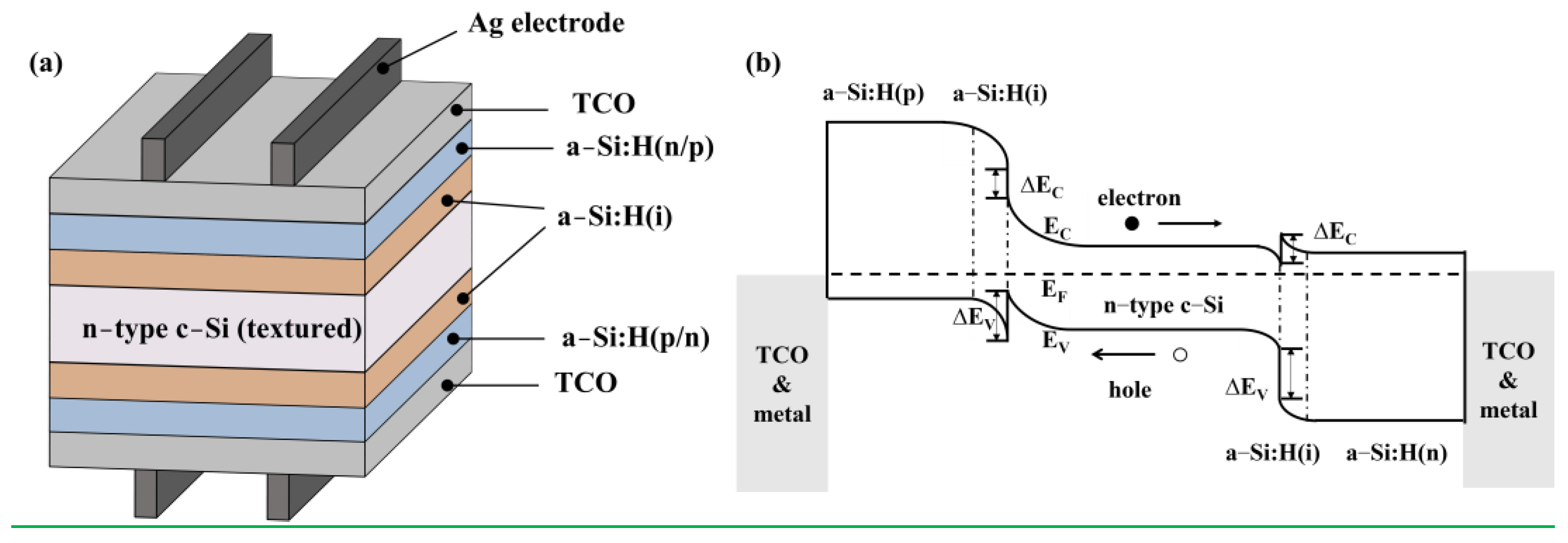
2.1. SHJ
2.2. Surface Cleaning Techniques
2.2.1. Radio Corporation of America (RCA) Standard Cleaning
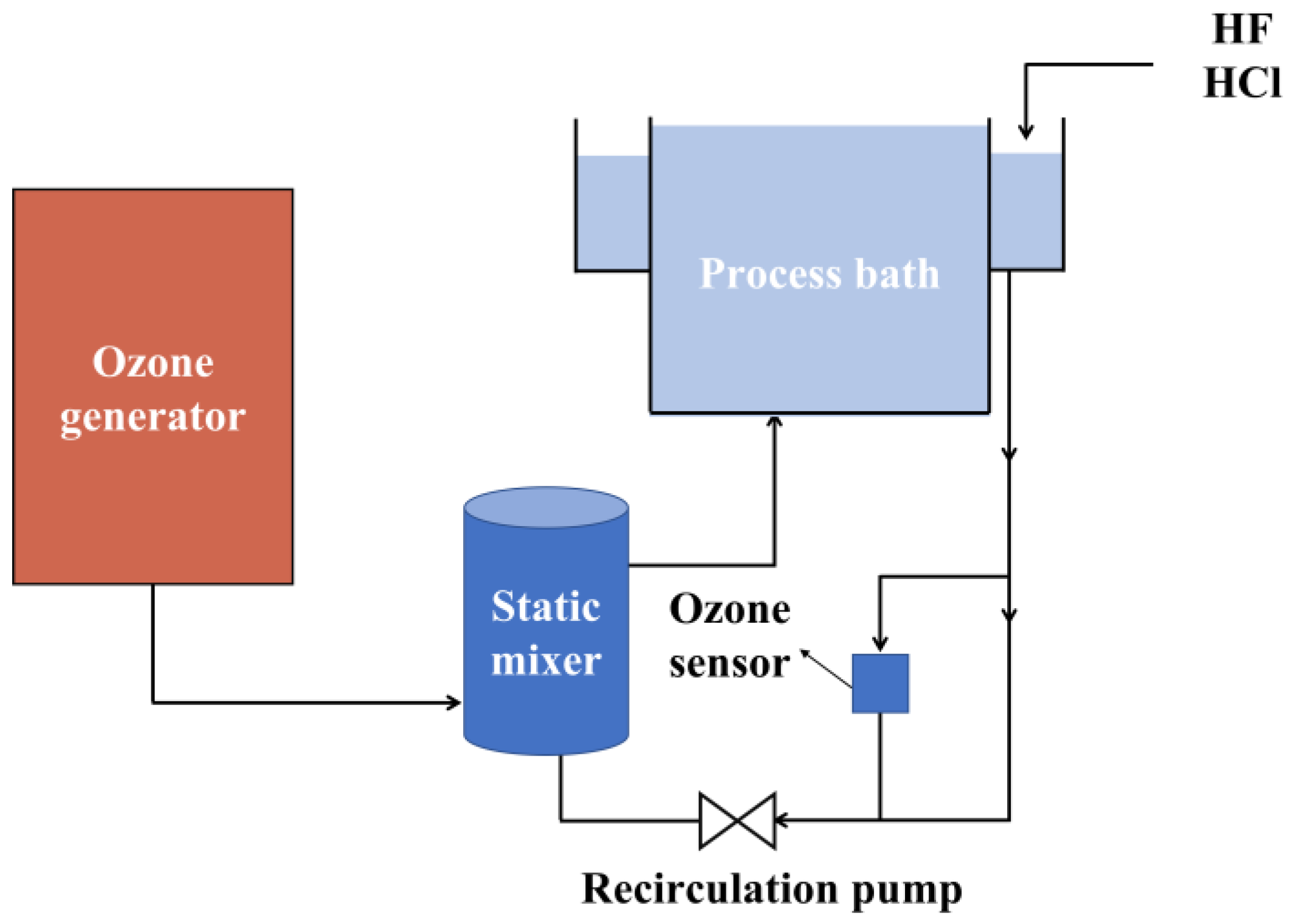
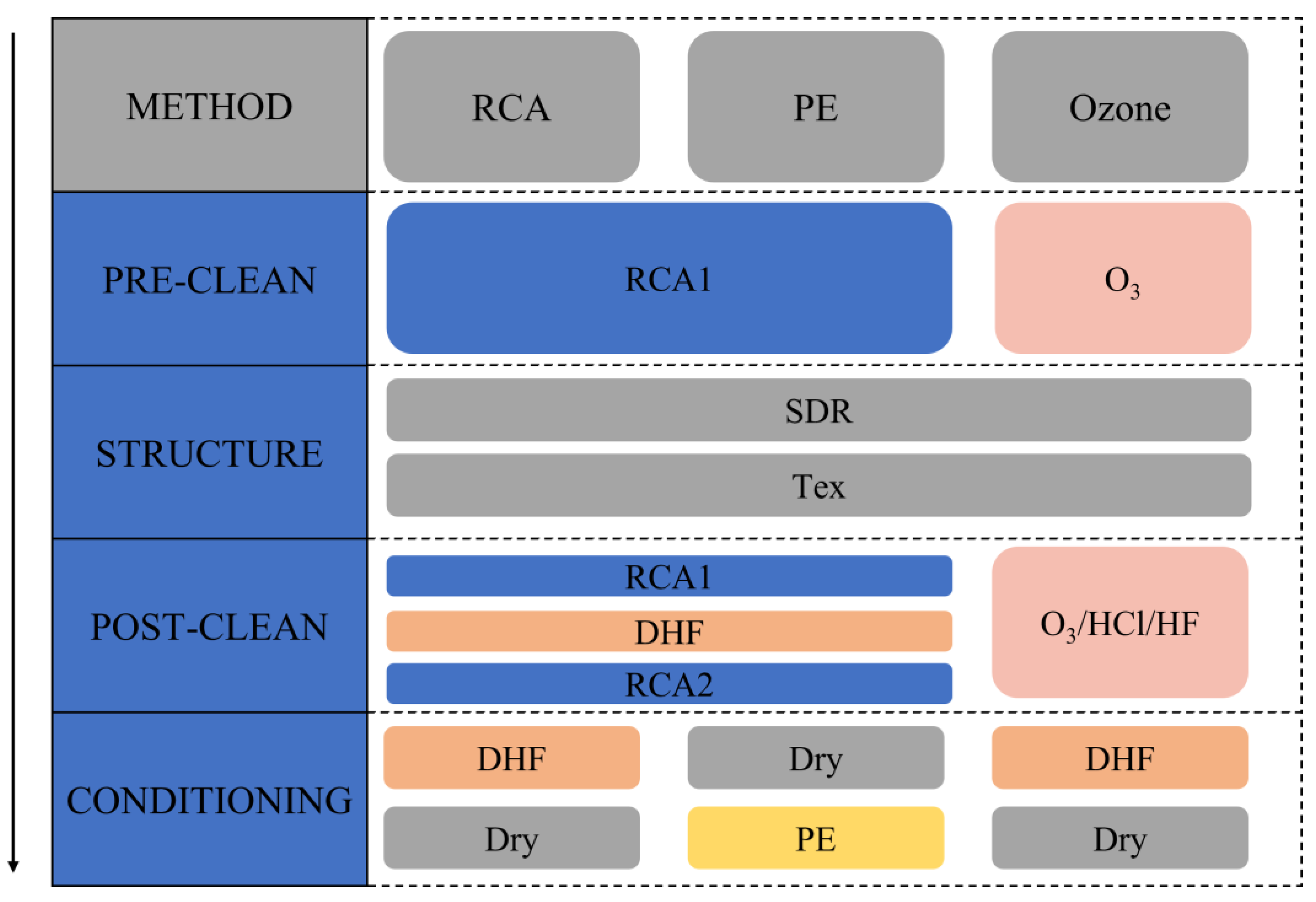
2.2.2. Ozone-Based Cleaning
2.2.3. Plasma Etching (PE)
2.3. Surface Passivation
2.3.1. Chemical Passivation
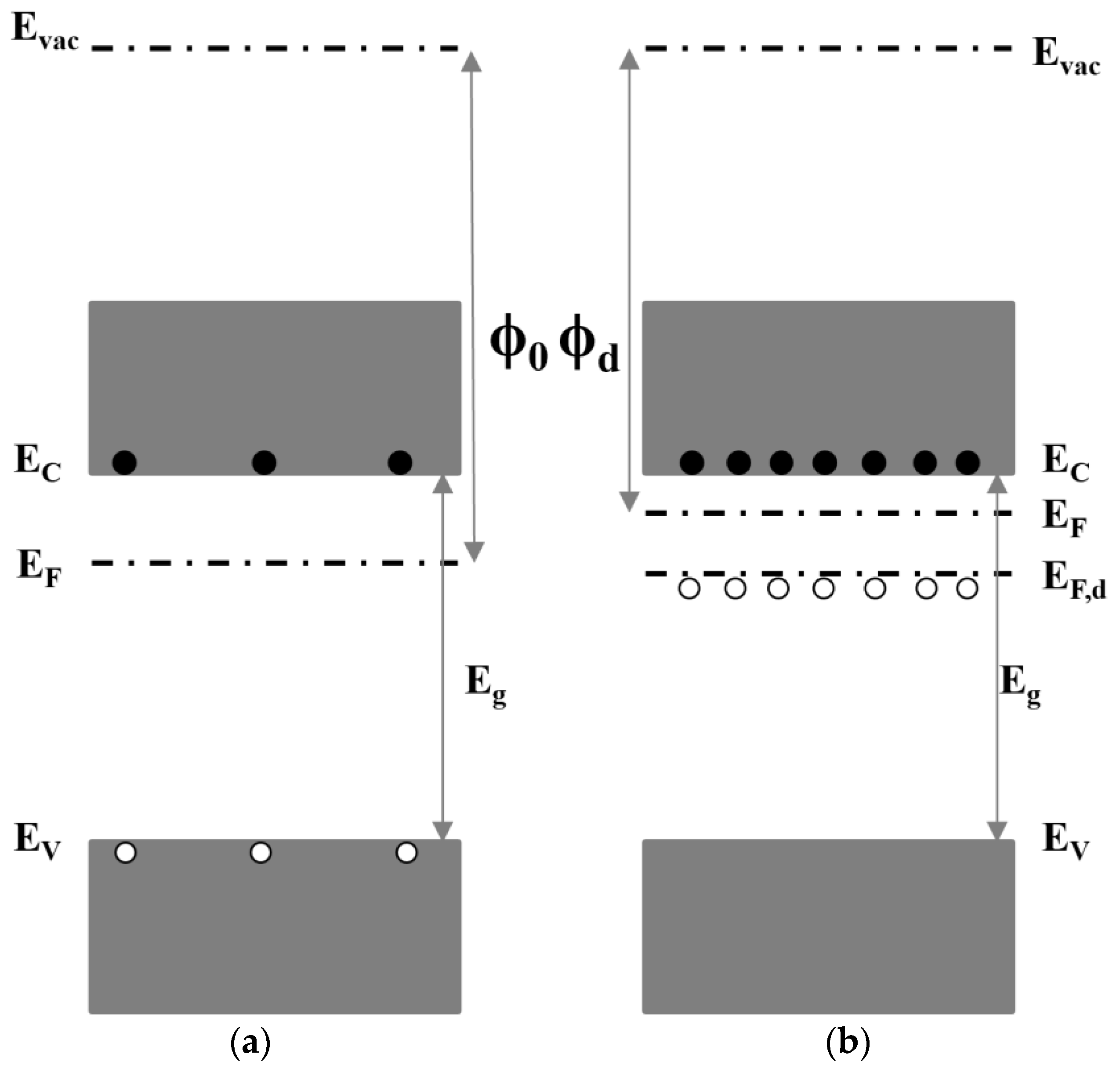
2.3.2. Field-Effect Passivation
- (1)
- Si-based materials:
- (2)
- Dopant-free materials:
3. Summary of Recent Highlights in High-Efficiency SHJ Solar Cells
4. Conclusions
Author Contributions
Funding
Institutional Review Board Statement
Informed Consent Statement
Data Availability Statement
Conflicts of Interest
References
- Renewable Energy Market Update-May 2022. Available online: https://www.iea.org (accessed on 4 June 2022).
- Singh, G. Solar power generation by PV (photovoltaic) technology: A review. Energy 2013, 53, 1–13. [Google Scholar] [CrossRef]
- Renewables 2021-Analysis and Forecast to 2026. Available online: https://www.iea.org/reports/renewables-2021 (accessed on 7 May 2022).
- The Global Energy Crisis Has Triggered Unprecedented Momentum behind Renewables, with the World Set to Add as Much Renewable Power in the Next 5 Years as It Did in the Past 20. Available online: https://www.iea.org/news/renewable-power-s-growth-is-being-turbocharged-as-countries-seek-to-strengthen-energy-security (accessed on 4 April 2023).
- Shen, W.; Zhao, Y.; Liu, F. Highlights of mainstream solar cell efficiencies in 2021. Front. Energy 2022, 16, 1–8. [Google Scholar] [CrossRef]
- Chunduri, S.K.; Schmela, M. Market Survey PERC Cell Production Equipment. TaiyangNews, 23 May 2022. [Google Scholar] [CrossRef]
- Masuko, K.; Shigematsu, M.; Hashiguchi, T.; Fujishima, D.; Kai, M.; Yoshimura, N.; Yamaguchi, T.; Ichihashi, Y.; Mishima, T.; Matsubara, N.; et al. Achievement of More Than 25% Conversion Efficiency with Crystalline Silicon Heterojunction Solar Cell. IEEE J. Photovolt. 2014, 4, 1433–1435. [Google Scholar] [CrossRef]
- Adachi, D.; Hernández, J.L.; Yamamoto, K. Impact of carrier recombination on fill factor for large area heterojunction crystalline silicon solar cell with 25.1% efficiency. Appl. Phys. Lett. 2015, 107, 233506. [Google Scholar] [CrossRef]
- Taguchi, M.; Yano, A.; Tohoda, S.; Matsuyama, K.; Nakamura, Y.; Nishiwaki, T.; Fujita, K.; Maruyama, E. 24.7% Record Efficiency HIT Solar Cell on Thin Silicon Wafer. IEEE J. Photovolt. 2014, 4, 96–99. [Google Scholar] [CrossRef]
- At 26.81%, LONGi Sets a New World Record Efficiency for Silicon Solar Celzls. Available online: https://www.longi.com/en/news/propelling-the-transformation/ (accessed on 9 February 2023).
- Smith, B.L.; Woodhouse, M.; Horowitz, K.A.W.; Silverman, T.J.; Zuboy, J.; Margolis, R.M. Photovoltaic (PV) Module Technologies: 2020 Benchmark Costs and Technology Evolution Framework Results. 2021. 2021. [Google Scholar] [CrossRef]
- Available online: https://infolink-group.com/market-report/ (accessed on 11 September 2022).
- Chunduri, S.K.; Schmela, M. Heterojunction Solar Technology Report 2023-Latest TaiyangNews HJT Report Edition Shows Progress across the Board as Stakeholders Work Hard On Cost Reduction. TaiyangNews, 24 March 2023. Available online: https://taiyangnews.info/(accessed on 4 April 2023).
- Liu, Z.; Sofia, S.E.; Laine, H.S.; Woodhouse, M.; Wieghold, S.; Peters, I.M.; Buonassisi, T. Revisiting thin silicon for photovoltaics: A technoeconomic perspective. Energy Environ. Sci. 2020, 13, 12–23. [Google Scholar] [CrossRef]
- Sai, H.; Umishio, H.; Matsui, T.; Nunomura, S.; Kawatsu, T.; Takato, H.; Matsubara, K. Impact of silicon wafer thickness on photovoltaic performance of crystalline silicon heterojunction solar cells. Jpn. J. Appl. Phys. 2018, 57, 08RB10. [Google Scholar] [CrossRef]
- Augusto, A.; Herasimenka, S.Y.; King, R.R.; Bowden, S.G.; Honsberg, C. Analysis of the recombination mechanisms of a silicon solar cell with low bandgap-voltage offset. J. Appl. Phys. 2017, 121, 205704. [Google Scholar] [CrossRef]
- Balaji, P.; Dauksher, W.J.; Bowden, S.G.; Augusto, A. Improving surface passivation on very thin substrates for high efficiency silicon heterojunction solar cells. Sol. Energy Mater. Sol. Cells 2020, 216, 110715. [Google Scholar] [CrossRef]
- Razzaq, A.; Allen, T.G.; Liu, W.; Liu, Z.; De Wolf, S. Silicon heterojunction solar cells: Techno-economic assessment and opportunities. Joule 2022, 6, 514–542. [Google Scholar] [CrossRef]
- Nagesh, M.; Suresh, R.; Jayapal, R.; Subramanya, K.N. Surface Passivation Studies of n-Type Crystalline Silicon for HIT Solar Cells. Trans. Electr. Electron. Mater. 2022, 23, 45–51. [Google Scholar] [CrossRef]
- Melskens, J.; van de Loo, B.W.H.; Macco, B.; Black, L.E.; Smit, S.; Kessels, W.M.M. Passivating Contacts for Crystalline Silicon Solar Cells: From Concepts and Materials to Prospects. IEEE J. Photovolt. 2018, 8, 373–388. [Google Scholar] [CrossRef]
- Panigrahi, J.; Komarala, V.K. Progress on the intrinsic a-Si:H films for interface passivation of silicon heterojunction solar cells: A review. J. Non-Cryst. Solids 2021, 574, 121166. [Google Scholar] [CrossRef]
- Sun, Z.; Chen, X.; He, Y.; Li, J.; Wang, J.; Yan, H.; Zhang, Y. Toward Efficiency Limits of Crystalline Silicon Solar Cells: Recent Progress in High-Efficiency Silicon Heterojunction Solar Cells. Adv. Energy Mater. 2022, 12, 2200015. [Google Scholar] [CrossRef]
- Muduli, S.P.; Kale, P. State-of-the-art passivation strategies of c-Si for photovoltaic applications: A review. Mater. Sci. Semicond. Process. 2023, 154, 107202. [Google Scholar] [CrossRef]
- Shockley, W. The Theory of p-n Junctions in Semiconductors and p-n Junction Transistors. Bell Syst. Tech. J. 1949, 28, 435–489. [Google Scholar] [CrossRef]
- Fuhs, W.; Niemann, K.; Stuke, J. Heterojunctions of Amorphous Silicon and Silicon Single Crystals. AIP Conf. Proc. 1974, 20, 345. [Google Scholar] [CrossRef]
- Tanaka, M.; Taguchi, M.; Matsuyama, T.; Sawada, T.; Tsuda, S.; Nakano, S.; Hanafusa, H.; Kuwano, Y. Development of New a-Si/c-Si Heterojunction Solar Cells: ACJ-HIT (Artificially Constructed Junction-Heterojunction with Intrinsic Thin-Layer). Jpn. J. Appl. Phys. 1992, 31, 3518–3522. [Google Scholar] [CrossRef]
- Sawada, T.; Terada, N.; Tsuge, S.; Baba, T.; Takahama, T.; Wakisaka, K.; Tsuda, S.; Nakano, S. High-efficiency a-Si/c-Si heterojunction solar cell. In Proceedings of the 1994 IEEE 1st World Conference on Photovoltaic Energy Conversion-WCPEC (A Joint Conference of PVSC, PVSEC and PSEC), Waikoloa, HI, USA, 5–9 December 1994. [Google Scholar] [CrossRef]
- De Nicolas, D.N. a-Si: H/c-Si Heterojunction Solar Cells: Back Side Assessment and Improvement. PhD Thesis, Université Paris Sud-Paris XI, Paris, France, December 2012. [Google Scholar]
- Descoeudres, A.; Holman, Z.C.; Barraud, L.; Morel, S.; De Wolf, S.; Ballif, C. >21% Efficient Silicon Heterojunction Solar Cells on n- and p-Type Wafers Compared. IEEE J. Photovolt. 2013, 3, 83–89. [Google Scholar] [CrossRef]
- Varache, R.; Kleider, J.P.; Favre, W.; Korte, L. Band bending and determination of band offsets in amorphous/crystalline silicon heterostructures from planar conductance measurements. J. Appl. Phys. 2012, 112, 123717. [Google Scholar] [CrossRef]
- Liang, T.S.; Pravettoni, M.; Deline, C.; Stein, J.S.; Kopecek, R.; Singh, J.P.; Luo, W.; Wang, Y.; Aberle, A.G.; Khoo, Y.S. A review of crystalline silicon bifacial photovoltaic performance characterisation and simulation. Energy Environ. Sci. 2019, 12, 116–148. [Google Scholar] [CrossRef]
- Taguchi, M.; Kawamoto, K.; Tsuge, S.; Baba, T.; Sakata, H.; Morizane, M.; Uchihashi, K.; Nakamura, N.; Kiyama, S.; Oota, O. HITTM cells—High-efficiency crystalline Si cells with novel structure. Prog. Photovolt. Res. Appl. 2000, 8, 503–513. [Google Scholar] [CrossRef]
- Ge, J.; Tang, M.; Wong, J.; Stangl, R.; Zhang, Z.; Dippell, T.; Doerr, M.; Hohn, O.; Huber, M.; Wohlfart, P.; et al. Investigation of Wide Process Temperature Window for Amorphous Silicon Suboxide Thin-Film Passivation Deposited by Inductively Coupled PECVD. IEEE J. Photovolt. 2015, 5, 705–710. [Google Scholar] [CrossRef]
- Zhang, L.; Guo, W.; Liu, W.; Bao, J.; Liu, J.; Shi, J.; Meng, F.; Liu, Z. Investigation of positive roles of hydrogen plasma treatment for interface passivation based on silicon heterojunction solar cells. J. Phys. D Appl. Phys. 2016, 49, 165305–165312. [Google Scholar] [CrossRef]
- Taguchi, M.; Terakawa, A.; Maruyama, E.; Tanaka, M. Obtaining a higherVoc in HIT cells. Prog. Photovolt. Res. Appl. 2005, 13, 481–488. [Google Scholar] [CrossRef]
- Kern, W. The Evolution of Silicon Wafer Cleaning Technology. J. Electrochem. Soc. 1990, 137, 1887. [Google Scholar] [CrossRef]
- Knotter, D.M. The Chemistry of Wet Cleaning. In Handbook of Cleaning in Semiconductor Manufacturing: Fundamental and Applications; Reinhardt, K.A., Reidy, R.F., Eds.; Scrivener Publishing LLC: Beverly, MA, USA, 2010; Chapter 2; pp. 115–160. [Google Scholar] [CrossRef]
- Buchholz, F.; Wefringhaus, E.; Plettig, M. Wet Chemical Cleaning for Industrial Application. In Photovoltaic Manufacturing: Etching, Texturing, and Cleaning; Müller, M.F., Ed.; Scrivener Publishing LLC: Beverly, MA, USA, 2021; Chapter 2; pp. 39–94. [Google Scholar] [CrossRef]
- Deligiannis, D.; Alivizatos, S.; Ingenito, A.; Zhang, D.; van Sebille, M.; van Swaaij, R.A.C.M.M.; Zeman, M. Wet-Chemical Treatment for Improved Surface Passivation of Textured Silicon Heterojunction Solar Cells. Energy Procedia 2014, 55, 197–202. [Google Scholar] [CrossRef]
- Strinitz, F.; El Jaouhari, A.; Schoerg, F.; Fuerst, M.; Plettig, M.; Kuehnlein, H. Advanced alkaline texturing and cleaning for PERC and SHJ solar cells. Energy Procedia 2017, 130, 23–30. [Google Scholar] [CrossRef]
- Trucks, G.W.; Raghavachari, K.; Higashi, G.S.; Chabal, Y.J. Mechanism of HF etching of silicon surfaces: A theoretical understanding of hydrogen passivation. Phys. Rev. Lett. 1990, 65, 504. [Google Scholar] [CrossRef]
- Lu, X.; Koppes, M.; Bronsveld, P.C.P. Simplified surface cleaning for fabrication of silicon heterojunction solar cells. AIP Conf. Proc. 2018, 1999, 050005. [Google Scholar] [CrossRef]
- De Smedt, F.; Vankerckhoven, H.; De Gendt, S.; Heyns, M.M.; Vinckier, C. Can We Increase the Efficiency of Organic Contamination Removal by Ozone/DI-Water Processes by Using Additives? Solid State Phenom. 2003, 92, 215–218. [Google Scholar] [CrossRef]
- Moldovan, A.; Birmann, K.; Rentsch, J.; Zimmer, M.; Gitte, T.; Fittkau, J. Combined Ozone/HF/HCI Based Cleaning and Adjusted Emitter Etch-Back for Silicon Solar Cells. Solid State Phenom. 2012, 195, 305–309. [Google Scholar] [CrossRef]
- Bergman, E.J.; Lagrange, S.; Claes, M.; De Gendt, S.; Röhr, E. Pre-Diffusion Cleaning Using Ozone and HF. Solid State Phenom. 2001, 76–77, 85–88. [Google Scholar] [CrossRef]
- Zou, S.; Xu, L.; Wu, C.; Ding, J.; Zhu, L.; Sun, H.; Ye, X.; Wang, X.; Zhang, X.; Su, X. Metal-catalyzed chemical etching using DIO3 as a hole injection agent for efficient submicron-textured multicrystalline silicon solar cells. Sol. Energy Mater. Sol. Cells 2021, 227, 111104. [Google Scholar] [CrossRef]
- Sonner, C.; Oltersdorf, A.; Zimmer, M.; Rentsch, J. Influence of contaminations and cleaning sequences on alkaline texturisation. In Proceedings of the 26th European PV Solar Energy Conference and Exhibition, Hamburg, Germany, 5–9 September 2011. [Google Scholar]
- Kranz, C.; Wyczanowski, S.; Baumann, U.; Dorn, S.; Queisser, S.; Schweckendiek, J.; Pysch, D.; Dullweber, T. Industrial Cleaning Sequences for Al2O3-Passivated PERC Solar Cells. Energy Procedia 2014, 55, 211–218. [Google Scholar] [CrossRef]
- Li, Z.; Yang, Y.; Zhang, X.; Feng, Z.; Verlinden, P.J. High-lifetime wafer cleaning method using ozone dissolved in DIW/HF/HCl solution. In Proceedings of the 29th European Photovoltaic Solar Energy Conference and Exhibition, Amsterdam, The Netherlands, 22–25 September 2014. [Google Scholar] [CrossRef]
- Zhang, Z.; Huber, M.; Corda, M. Key Equipments for O3-Based Wet-Chemical Surface Engineering and PVD Processes Tailored for High-Efficiency Silicon Heterojunction Solar Cells. Energy Procedia 2017, 130, 31–35. [Google Scholar] [CrossRef]
- Chunduri, S.K.; Schmela, M. Heterojunction Solar Technology 2019 Edition—The Next Big Thing in Solar Cell/Module Manufacturing. TaiyangNews, 20 March 2019. [Google Scholar] [CrossRef]
- Liu, W.; Meng, F.; Zhang, X.; Liu, Z. Evolution of a Native Oxide Layer at the a-Si:H/c-Si Interface and Its Influence on a Silicon Heterojunction Solar Cell. ACS Appl. Mater. Interfaces 2015, 7, 26522–26529. [Google Scholar] [CrossRef]
- Moreno, M.; Labrune, M.; Cabarrocas, P.R. Dry fabrication process for heterojunction solar cells through in-situ plasma cleaning and passivation. Sol. Energy Mater. Sol. Cells 2010, 94, 402–405. [Google Scholar] [CrossRef]
- Tang, M.; Ge, J.; Wong, J.; Liu, Z.; Dippell, T.; Zhang, Z.; Huber, M.; Doerr, M.; Hohn, O.; Wohlfart, P.; et al. Investigation of Low-Temperature Hydrogen Plasma-Etching Processes for Silicon Wafer Solar Cell Surface Passivation in an Industrial Inductively Coupled Plasma Deposition Tool. IEEE J. Photovolt. 2015, 6, 10–16. [Google Scholar] [CrossRef]
- Chang, R.P.H.; Chang, C.C.; Darack, S. Hydrogen plasma etching of semiconductors and their oxides. J. Vac. Sci. Technol. 1982, 20, 45–50. [Google Scholar] [CrossRef]
- Tang, M.; Ge, J.; Wong, J.; Ling, Z.P.; Dippell, T.; Zhang, Z.; Huber, M.; Doerr, M.; Hohn, O.; Wohlfart, P.; et al. Excellent passivation of thin silicon wafers by HF-free hydrogen plasma etching using an industrial ICPECVD tool. Phys. Status Solidi RRL 2015, 9, 47–52. [Google Scholar] [CrossRef]
- Xu, M.; Wang, C.; Bearda, T.; Simoen, E.; Radhakrishnan, H.S.; Gordon, I.; Li, W.; Szlufcik, J.; Poortmans, J. Dry Passivation Process for Silicon Heterojunction Solar Cells Using Hydrogen Plasma Treatment Followed by in Situ a-Si:H Deposition. IEEE J. Photovolt. 2018, 8, 1539–1545. [Google Scholar] [CrossRef]
- Geissbühler, J.; De Wolf, S.; Demaurex, B.; Seif, J.P.; Alexander, D.; Barraud, L.; Ballif, C. Amorphous/crystalline silicon interface defects induced by hydrogen plasma treatments. Appl. Phys. Lett. 2013, 102, 231604. [Google Scholar] [CrossRef]
- Lee, S.; Trinh, T.T.; Pham, D.P.; Kim, S.; Kim, Y.; Park, J.; Nam, N.D.; Dao, V.-A.; Yi, j. In Situ Process to Form Passivated Tunneling Oxides for Front-Surface Field in Rear-Emitter Silicon Heterojunction Solar Cells. ACS Sustain. Chem. Eng. 2019, 7, 19332–19337. [Google Scholar] [CrossRef]
- Acharyya, S.; Sadhukhan, S.; Panda, T.; Ghosh, D.K.; Mandal, N.C.; Nandi, A.; Bose, S.; Das, G.; Maity, S.; Chaudhuri, P.; et al. Dopant-free materials for carrier-selective passivating contact solar cells: A review. Surf. Interfaces 2022, 28, 101687. [Google Scholar] [CrossRef]
- Schmidt, M.; Korte, L.; Laades, A.; Stangl, R.; Schubert, C.; Angermann, H.; Conrad, E.; Maydell, K. Physical aspects of a-Si:H/c-Si hetero-junction solar cells. Thin Solid Film. 2007, 515, 7475–7480. [Google Scholar] [CrossRef]
- Weinberger, B.R.; Deckman, H.W.; Yablonovitch, E.; Gmitter, T.J.; Kobasz, W.; Garoff, S. The passivation of electrically active sites on the surface of crystalline silicon by fluorination. J. Vac. Sci. Technol. A 1985, 3, 887–891. [Google Scholar] [CrossRef]
- Chabal, Y.J.; Higashi, G.S.; Raghavachari, K.; Burrows, V.A. Infrared spectroscopy of Si(111) and Si(100) surfaces after HF treatment: Hydrogen termination and surface morphology. J. Vac. Sci. Technol. A 1989, 7, 2104–2109. [Google Scholar] [CrossRef]
- Yablonovitch, E.; Allara, D.L.; Chang, C.C.; Gmitter, T.; Bright, T.B. Unusually Low Surface-Recombination Velocity on Silicon and Germanium Surfaces. Phys. Rev. Lett. 1986, 57, 249–252. [Google Scholar] [CrossRef]
- Fujiwara, H.; Kondo, M. Impact of epitaxial growth at the heterointerface of a-Si:H/c-Si solar cells. Appl. Phys. Lett. 2007, 90, 013503. [Google Scholar] [CrossRef]
- Chu, Y.-H.; Lee, C.-C.; Chang, T.-H.; Chang, S.-Y.; Chang, J.-Y.; Li, T.; Chen, I.-C. Investigation of hydrogenated amorphous silicon as passivation layer by high density plasma. Thin Solid Film. 2014, 570, 591–594. [Google Scholar] [CrossRef]
- De Wolf, S.; Kondo, M. Abruptness of a-Si:H/c-Si interface revealed by carrier lifetime measurements. Appl. Phys. Lett. 2007, 90, 042111. [Google Scholar] [CrossRef]
- De Wolf, S.; Kondo, M. Nature of doped a-Si:H/c-Si interface recombination. J. Appl. Phys. 2009, 105, 103707. [Google Scholar] [CrossRef]
- De Wolf, S.; Kondo, M. Boron-doped a-Si:H/c-Si interface passivation: Degradation mechanism. Appl. Phys. Lett. 2007, 91, 112109. [Google Scholar] [CrossRef]
- Liu, W.; Zhang, L.; Chen, R.; Meng, F.; Guo, W.; Bao, J.; Liu, Z. Underdense a-Si:H film capped by a dense film as the passivation layer of a silicon heterojunction solar cell. J. Appl. Phys. 2016, 120, 175301. [Google Scholar] [CrossRef]
- Wu, Z.; Zhang, L.; Liu, W.; Chen, R.; Li, Z.; Meng, F.; Liu, Z. Role of hydrogen in modifying a-Si:H/c-Si interface passivation and band alignment for rear-emitter silicon heterojunction solar cells. J. Mater. Sci. Mater. Electron. 2020, 31, 9468–9474. [Google Scholar] [CrossRef]
- Wu, Z.; Zhang, L.; Chen, R.; Liu, W.; Li, Z.; Meng, F.; Liu, Z. Improved amorphous/crystalline silicon interface passivation for silicon heterojunction solar cells by hot-wire atomic hydrogen during doped a-Si:H deposition. Appl. Surf. Sci. 2019, 475, 504–509. [Google Scholar] [CrossRef]
- Sai, H.; Matsui, T.; Nunomura, S.; Matsubara, K. Interplay between intrinsic bi-layers and overlying doped layers in a-Si:H/c-Si heterojunction solar cells. In Proceedings of the 2018 IEEE 7th World Conference on Photovoltaic Energy Conversion (WCPEC)(A Joint Conference of 45th IEEE PVSC, 28th PVSEC & 34th EU PVSEC), Waikoloa, HI, USA, 10–15 June 2018. [Google Scholar] [CrossRef]
- Luderer, C.; Kurt, D.; Moldovan, A.; Hermle, M.; Bivour, M. Intrinsic layer modification in silicon heterojunctions: Balancing transport and surface passivation. Sol. Energy Mater. Sol. Cells 2022, 238, 111412. [Google Scholar] [CrossRef]
- Chen, P.-W.; Hsu, H.-J.; Matsui, T.; Nunomura, S.; Matsubara, K. Impact of intrinsic amorphous silicon bilayers in silicon heterojunction solar cells. J. Appl. Phys. 2018, 124, 103102. [Google Scholar] [CrossRef]
- Zhao, L.; Diao, H.; Zeng, X.; Zhou, C.; Li, H.; Wang, W. Comparative study of the surface passivation on crystalline silicon by silicon thin films with different structures. Phys. B Condens. Matter 2010, 405, 61–64. [Google Scholar] [CrossRef]
- Kim, S.; Dao, V.A.; Shin, C.; Cho, J.; Lee, Y.; Balaji, N.; Ahn, S.; Kim, Y.; Yi, J. Low defect interface study of intrinsic layer for c-Si surface passivation in a-Si:H/c-Si heterojunction solar cells. Thin Solid Film. 2012, 521, 45–49. [Google Scholar] [CrossRef]
- Ruan, T.; Qu, M.; Qu, X.; Ru, X.; Wang, J.; He, Y.; Zheng, K.; Lin, B.H.H.; Xu, X.; Zhang, Y.; et al. Achieving high efficiency silicon heterojunction solar cells by applying high hydrogen content amorphous silicon as epitaxial-free buffer layers. Thin Solid Film. 2020, 711, 138305. [Google Scholar] [CrossRef]
- Yu, Z.; Pereyra, I.; Carreno, M. Wide optical band gap window layers for solar cells. Sol. Energy Mater. Sol. Cells 2001, 66, 155–162. [Google Scholar] [CrossRef]
- Kaminski, P.; Abbas, A.; Bass, K.; Claudio, G. Passivation of silicon wafers by Silicon Carbide (SiCx) thin film grown by sputtering. Energy Procedia 2011, 10, 71–75. [Google Scholar] [CrossRef]
- Donercark, E.; Sedani, S.H.; Kabaçelik, I.; Salimi, A.; Turan, R. Interface and material properties of wide band gap a-SiCx:H thin films for solar cell applications. Renew. Energy 2022, 183, 781–790. [Google Scholar] [CrossRef]
- Ehling, C.; Treptow, D.; Bilger, G.; Einsele, F.; Schubert, M.B. Electronic surface passivation of crystalline silicon solar cells by a-SiC:H. In Proceedings of the 2010 35th IEEE Photovoltaic Specialists Conference, Honolulu, HI, USA, 20–25 June 2010. [Google Scholar] [CrossRef]
- Iftiquar, S.M. The roles of deposition pressure and rf power in opto-electronic properties of a-SiO:H films. J. Phys. D Appl. Phys. 1998, 31, 1630–1641. [Google Scholar] [CrossRef]
- Jiang, K.; Liu, W.; Yang, Y.; Yan, Z.; Huang, S.; Li, Z.; Li, X.; Zhang, L.; Liu, Z. Functions of oxygen atoms in hydrogenated amorphous silicon oxide layers for rear-emitter silicon heterojunction solar cells. J. Mater. Sci. Mater. Electron. 2022, 33, 416–426. [Google Scholar] [CrossRef]
- Fujiwara, H.; Kaneko, T.; Kondo, M. Application of hydrogenated amorphous silicon oxide layers to c-Si heterojunction solar cells. Appl. Phys. Lett. 2007, 91, 133508. [Google Scholar] [CrossRef]
- Jiang, K.; Yang, Y.; Yan, Z.; Huang, S.; Li, X.; Li, Z.; Zhou, Y.; Zhang, L.; Meng, F.; Liu, Z.; et al. Balance of efficiency and stability of silicon heterojunction solar cells. Sol. Energy Mater. Sol. Cells 2022, 243, 111801. [Google Scholar] [CrossRef]
- Zhang, B.; Zhang, Y.; Cong, R.; Li, Y.; Yu, W.; Fu, G. Superior silicon surface passivation in HIT solar cells by optimizing a-SiOx:H thin films: A compact intrinsic passivation layer. Sol. Energy 2017, 155, 670–678. [Google Scholar] [CrossRef]
- Nogay, G.; Seif, J.P.; Riesen, Y.; Tomasi, A.; Jeangros, Q.; Wyrsch, N.; Haug, F.-J.; De Wolf, S.; Ballif, C. Nanocrystalline Silicon Carrier Collectors for Silicon Heterojunction Solar Cells and Impact on Low-Temperature Device Characteristics. IEEE J. Photovolt. 2016, 6, 1654–1662. [Google Scholar] [CrossRef]
- Holman, Z.C.; Descoeudres, A.; Barraud, L.; Fernandez, F.Z.; Seif, J.P.; De Wolf, S.; Ballif, C. Current Losses at the Front of Silicon Heterojunction Solar Cells. IEEE J. Photovolt. 2012, 2, 7–15. [Google Scholar] [CrossRef]
- Cabarrocas, P.R.; Morral, A.F.; Kalache, B.; Kasouit, S. Microcrystalline Silicon Thin-Films Grown by Plasma Enhanced Chemical Vapour Deposition—Growth Mechanisms and Grain Size Control. Solid State Phenom. 2003, 93, 257–268. [Google Scholar] [CrossRef]
- Gabriel, O.; Kirner, S.; Klingsporn, M.; Friedrich, F.; Stannowski, B.; Schlatmann, R. On the Plasma Chemistry during Plasma Enhanced Chemical Vapor Deposition of Microcrystalline Silicon Oxides. Plasma Process. Polym. 2015, 12, 82–91. [Google Scholar] [CrossRef]
- Das, D.; Bhattacharya, K. Characterization of the Si:H network during transformation from amorphous to micro- and nanocrystalline structures. J. Appl. Phys. 2006, 100, 103701. [Google Scholar] [CrossRef]
- Myong, S.Y.; Lee, H.K.; Yoon, E.; Lim, K.S. Highly conductive boron-doped nanocrystalline silicon-carbide film prepared by low-hydrogen-dilution photo-CVD method using ethylene as a carbon source. J. Non-Cryst. Solids 2002, 298, 131–136. [Google Scholar] [CrossRef]
- Sharma, M.; Panigrahi, J.; Komarala, V.K. Nanocrystalline silicon thin film growth and application for silicon heterojunction solar cells: A short review. Nanoscale Adv. 2021, 3, 3373–3383. [Google Scholar] [CrossRef] [PubMed]
- Zhang, Y.; Cong, R.; Zhao, W.; Li, Y.; Jin, C.; Yu, W.; Fu, G. Improved hetero-interface passivation by microcrystalline silicon oxide emitter in silicon heterojunction solar cells. Sci. Bull. 2016, 61, 787–793. [Google Scholar] [CrossRef]
- Sen, C.-D.; Son, J.-I.; Kim, H.-H.; Yun, H.-S.; Cho, N.-H. Variation of the nanostructural feature of nc-SiC:H thin films with post-deposition thermal annealing. Thin Solid Film. 2014, 571, 238–244. [Google Scholar] [CrossRef]
- Köhler, M.; Pomaska, M.; Procel, P.; Santbergen, R.; Zamchiy, A.; Macco, B.; Lambertz, A.; Duan, W.; Cao, P.; Klingebiel, B.; et al. A silicon carbide-based highly transparent passivating contact for crystalline silicon solar cells approaching efficiencies of 24%. Nat. Energy 2021, 6, 529–537. [Google Scholar] [CrossRef]
- Köhler, M.; Zamchiy, A.; Pomaska, M.; Lambertz, A.; Lentz, F.; Duan, W.; Smirnov, V.; Finger, F.; Rau, U.; Ding, K. Development of a transparent passivated contact as a front side contact for silicon heterojunction solar cells. In Proceedings of the 2018 IEEE 7th World Conference on Photovoltaic Energy Conversion (WCPEC)(A Joint Conference of 45th IEEE PVSC, 28th PVSEC & 34th EU PVSEC), Waikoloa, HI, USA, 10–15 June 2018. [Google Scholar] [CrossRef]
- Pomaska, M.; Beyer, W.; Neumann, E.; Finger, F.; Ding, K. Impact of microcrystalline silicon carbide growth using hot-wire chemical vapor deposition on crystalline silicon surface passivation. Thin Solid Film. 2015, 595, 217–220. [Google Scholar] [CrossRef]
- Cho, J.-S.; Jang, E.; Lim, D.; Ahn, S.; Yoo, J.; Cho, A.; Park, J.H.; Kim, K.; Choi, B.-H. Wide-bandgap nanocrystalline silicon-carbon alloys for photovoltaic applications. Sol. Energy Mater. Sol. Cells 2018, 182, 220–227. [Google Scholar] [CrossRef]
- Ghahfarokhi, O.M.; von Maydell, K.; Agert, C. Enhanced passivation at amorphous/crystalline silicon interface and suppressed Schottky barrier by deposition of microcrystalline silicon emitter layer in silicon heterojunction solar cells. Appl. Phys. Lett. 2014, 104, 113901. [Google Scholar] [CrossRef]
- Cabarrocas, P.R.; Layadi, N.; Heitz, T.; Drévillon, B.; Solomon, I. Substrate selectivity in the formation of microcrystalline silicon: Mechanisms and technological consequences. Appl. Phys. Lett. 1995, 66, 3609–3611. [Google Scholar] [CrossRef]
- Mazzarella, L.; Morales-Vilches, A.; Korte, L.; Schlatmann, R.; Stannowski, B. Ultra-thin nanocrystalline n-type silicon oxide front contact layers for rear-emitter silicon heterojunction solar cells. Sol. Energy Mater. Sol. Cells 2018, 179, 386–391. [Google Scholar] [CrossRef]
- Pham, D.P.; Kim, S.; Lee, S.; Le, A.H.T.; Cho, E.-C.; Park, J.; Yi, J. Controlling a crystalline seed layer for mirocrystalline silicon oxide window layer in rear emitter silicon heterojunction cells. Infrared Phys. Technol. 2019, 102, 103037. [Google Scholar] [CrossRef]
- Seif, J.P.; Descoeudres, A.; Nogay, G.; Hanni, S.; de Nicolas, S.M.; Holm, N.; Geissbuhler, J.; Hessler-Wyser, A.; Duchamp, M.; Dunin-Borkowski, R.E.; et al. Strategies for Doped Nanocrystalline Silicon Integration in Silicon Heterojunction Solar Cells. IEEE J. Photovolt. 2016, 6, 1132–1140. [Google Scholar] [CrossRef]
- Bullock, J.; Hettick, M.; Geissbühler, J.; Ong, A.J.; Allen, T.; Sutter-Fella, C.M.; Chen, T.; Ota, H.; Schaler, E.W.; De Wolf, S.; et al. Efficient silicon solar cells with dopant-free asymmetric heterocontacts. Nat. Energy 2016, 1, 1. [Google Scholar] [CrossRef]
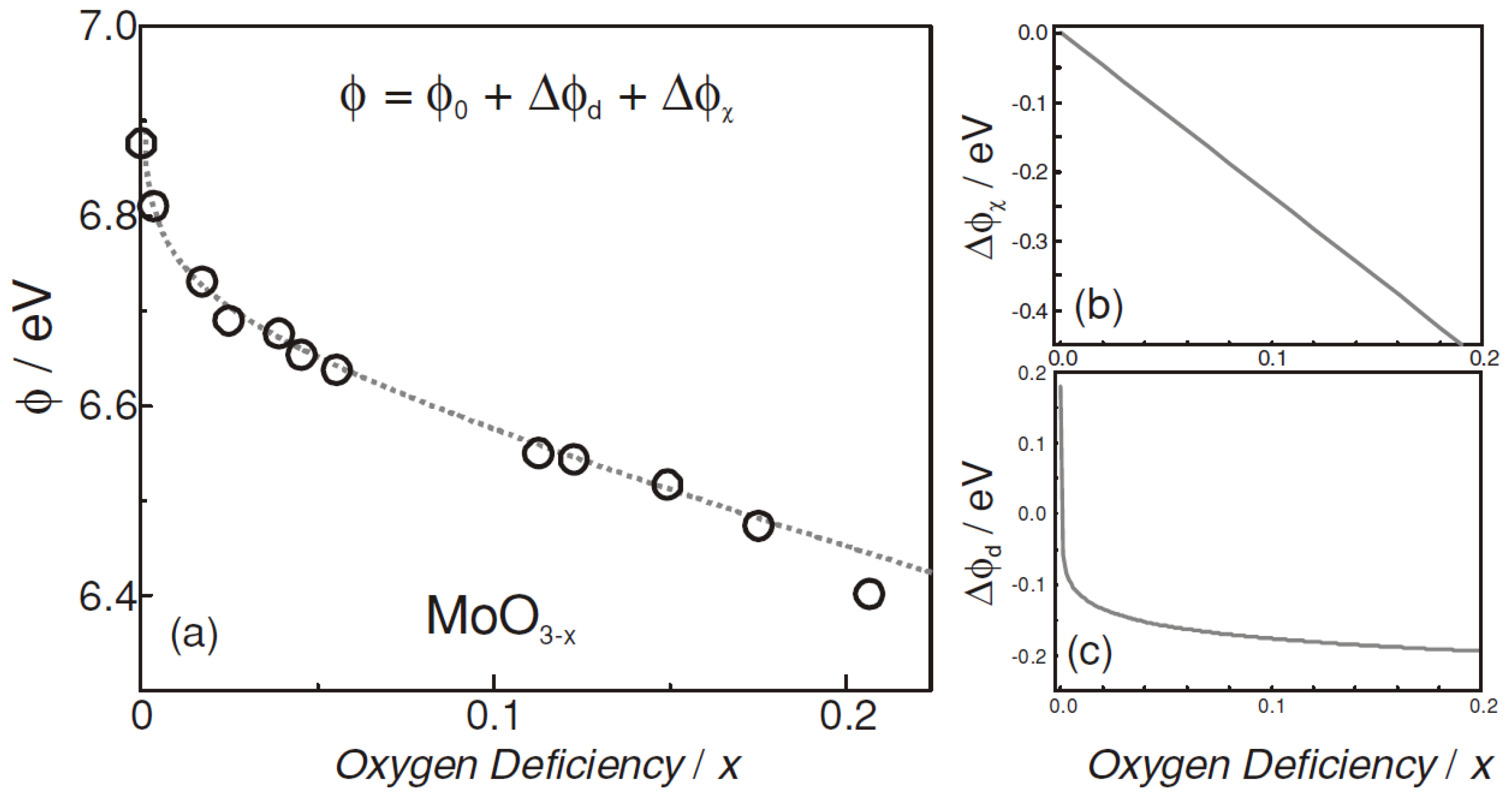
- Mews, M.; Korte, L.; Rech, B. Oxygen vacancies in tungsten oxide and their influence on tungsten oxide/silicon heterojunction solar cells. Sol. Energy Mater. Sol. Cells 2016, 158, 77–83. [Google Scholar] [CrossRef]
- Song, Y.; Li, X.; Mackin, C.; Zhang, X.; Fang, W.; Palacios, T.; Zhu, H.; Kong, J. Role of Interfacial Oxide in High-Efficiency Graphene-Silicon Schottky Barrier Solar Cells. Nano Lett. 2015, 15, 2104–2110. [Google Scholar] [CrossRef]
- MacQueen, R.W.; Liebhaber, M.; Niederhausen, J.; Mews, M.; Gersmann, C.; Jäckle, S.; Jäger, K.; Tayebjee, M.J.Y.; Schmidt, T.W.; Rech, B.; et al. Crystalline silicon solar cells with tetracene interlayers: The path to silicon-singlet fission heterojunction devices. Mater. Horiz. 2018, 5, 1065–1075. [Google Scholar] [CrossRef]
- Gerling, L.G.; Mahato, S.; Morales-Vilches, A.; Masmitja, G.; Ortega, P.; Voz, C.; Alcubilla, R.; Puigdollers, J. Transition metal oxides as hole-selective contacts in silicon heterojunctions solar cells. Sol. Energy Mater. Sol. Cells 2016, 145, 109–115. [Google Scholar] [CrossRef]
- Almora, O.; Gerling, L.G.; Voz, C.; Alcubilla, R.; Puigdollers, J.; Garcia-Belmonte, G. Superior performance of V2O5 as hole selective contact over other transition metal oxides in silicon heterojunction solar cells. Sol. Energy Mater. Sol. Cells 2017, 168, 221–226. [Google Scholar] [CrossRef]
- Wu, W.; Bao, J.; Jia, X.; Liu, Z.; Cai, L.; Liu, B.; Song, J.; Shen, H. Dopant-free back contact silicon heterojunction solar cells employing transition metal oxide emitters. Phys. Status Solidi RRL 2016, 10, 662–667. [Google Scholar] [CrossRef]
- Gao, P.; Yang, Z.; He, J.; Yu, J.; Liu, P.; Zhu, J.; Ge, Z.; Ye, J. Dopant-Free and Carrier-Selective Heterocontacts for Silicon Solar Cells: Recent Advances and Perspectives. Adv. Sci. 2018, 5, 1700547. [Google Scholar] [CrossRef]
- Bullock, J.; Cuevas, A.; Allen, T.; Battaglia, C. Molybdenum oxide MoOx: A versatile hole contact for silicon solar cells. Appl. Phys. Lett. 2014, 105, 232109. [Google Scholar] [CrossRef]
- Sacchetto, D.; Jeangros, Q.; Christmann, G.; Barraud, L.; Descoeudres, A.; Geissbuhler, J.; Despeisse, M.; Hessler-Wyser, A.; Nicolay, S.; Ballif, C. ITO/MoOx/a-Si:H(i) Hole-Selective Contacts for Silicon Heterojunction Solar Cells: Degradation Mechanisms and Cell Integration. IEEE J. Photovolt. 2017, 7, 1584–1590. [Google Scholar] [CrossRef]
- Geissbühler, J.; Werner, J.; de Nicolas, S.M.; Barraud, L.; Hessler-Wyser, A.; Despeisse, M.; Nicolay, S.; Tomasi, A.; Niesen, B.; De Wolf, S.; et al. 22.5% efficient silicon heterojunction solar cell with molybdenum oxide hole collector. Appl. Phys. Lett. 2015, 107, 081601. [Google Scholar] [CrossRef]
- Battaglia, C.; de Nicolás, S.M.; De Wolf, S.; Yin, X.; Zheng, M.; Ballif, C.; Javey, A. Silicon heterojunction solar cell with passivated hole selective MoOx contact. Appl. Phys. Lett. 2014, 104, 113902. [Google Scholar] [CrossRef]
- Wang, F.; Zhao, S.; Liu, B.; Li, Y.; Ren, Q.; Du, R.; Wang, N.; Wei, C.; Chen, X.; Wang, G.; et al. Silicon solar cells with bifacial metal oxides carrier selective layers. Nano Energy 2017, 39, 437–443. [Google Scholar] [CrossRef]
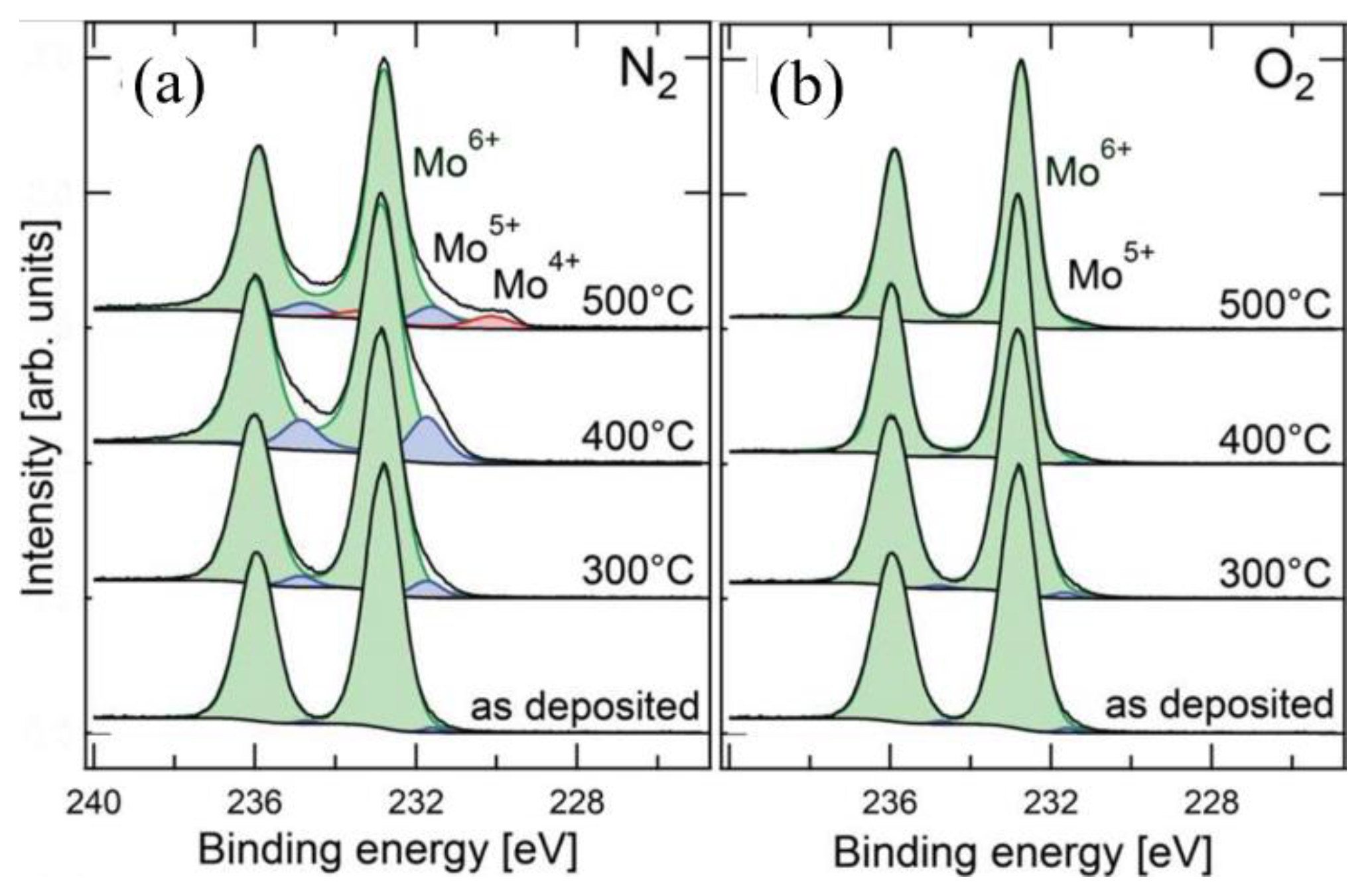
- Khokhar, M.Q.; Mallem, K.; Fan, X.; Kim, Y.; Hussain, S.Q.; Cho, E.-C.; Yi, J. Experimental and Numerical Simulation of Molybdenum Oxide Films with Wide Bandgap and High Work Function for Carrier-Selective Contact Solar Cells. ECS J. Solid State Sci. Technol. 2022, 11, 085001. [Google Scholar] [CrossRef]
- Yu, J.; Fu, Y.; Zhu, L.; Yang, Z.; Yang, X.; Ding, L.; Zeng, Y.; Yan, B.; Tang, J.; Gao, P.; et al. Heterojunction solar cells with asymmetrically carrier-selective contact structure of molybdenum-oxide/silicon/magnesium-oxide. Sol. Energy 2018, 159, 704–709. [Google Scholar] [CrossRef]
- Kumar, M.; Cho, E.-C.; Prodanov, M.F.; Kang, C.; Srivastava, A.K.; Yi, J. MoOx work function, interface structure, and thermal stability analysis of ITO/MoOx/a-Si(i) stacks for hole-selective silicon heterojunction solar cells. Appl. Surf. Sci. 2021, 553, 149552. [Google Scholar] [CrossRef]
- Mehmood, H.; Nasser, H.; Ozkol, E.; Tauqeer, T.; Hussain, S.; Turan, R. Physical device simulation of partial dopant-free asymmetric silicon heterostructure solar cell (P-DASH) based on hole-selective Molybdenum oxide (MoOx) with Crystalline Silicon (cSi). In Proceedings of the 2017 International Conference on Engineering and Technology (ICET), Antalya, Turkey, 21–23 August 2017. [Google Scholar] [CrossRef]
- Battaglia, C.; Yin, X.; Zheng, M.; Sharp, I.D.; Chen, T.; McDonnell, S.; Azcatl, A.; Carraro, C.; Ma, B.; Maboudian, R.; et al. Hole Selective MoOx Contact for Silicon Solar Cells. Nano Lett. 2014, 14, 967–971. [Google Scholar] [CrossRef] [PubMed]
- Gerling, L.; Mahato, S.; Voz, C.; Alcubilla, R.; Puigdollers, J. Characterization of Transition Metal Oxide/Silicon Heterojunctions for Solar Cell Applications. Appl. Sci. 2015, 5, 695–705. [Google Scholar] [CrossRef]
- Greiner, M.T.; Chai, L.; Helander, M.G.; Tang, W.-M.; Lu, Z.-H. Transition Metal Oxide Work Functions: The Influence of Cation Oxidation State and Oxygen Vacancies. Adv. Funct. Mater. 2012, 22, 4557–4568. [Google Scholar] [CrossRef]
- Davis, B.E.; Strandwitz, N.C. Aluminum Oxide Passivating Tunneling Interlayers for Molybdenum Oxide Hole-Selective Contacts. IEEE J. Photovolt. 2020, 10, 722–728. [Google Scholar] [CrossRef]
- Han, B.; Gao, M.; Wan, Y.; Li, Y.; Song, W.; Ma, Z. Effect of post-annealing on the properties of thermally evaporated molybdenum oxide films: Interdependence of work function and oxygen to molybdenum ratio. Mater. Sci. Semicond. Process. 2018, 75, 166–172. [Google Scholar] [CrossRef]
- Chen, J.; Liu, C.; Xu, S.; Wang, P.; Ge, X.; Han, B.; Zhang, Y.; Wang, M.; Wu, X.; Xu, L.; et al. Solution-processed molybdenum oxide films by low-temperature annealing for improved silicon surface passivation. Mater. Sci. Semicond. Process. 2021, 132, 105920. [Google Scholar] [CrossRef]
- Behera, G.; Vikram; Kumar, A.; Balasubramaniam, K.; Alam, A. First-Principles Study of the Surface Passivation Effect in the Si/MoOx Interface. J. Phys. Chem. C 2021, 125, 11513–11523. [Google Scholar] [CrossRef]
- Singh, K.; Singh, D.K.; Komarala, V.K. Numerical simulations of carrier-selective contact silicon solar cells: Role of carrier-selective layers electronic properties. J. Comput. Electron. 2021, 20, 1815–1821. [Google Scholar] [CrossRef]
- Bullock, J.; Wan, Y.; Xu, Z.; Essig, S.; Hettick, M.; Wang, H.; Ji, W.; Boccard, M.; Cuevas, A.; Ballif, C.; et al. Stable Dopant-Free Asymmetric Heterocontact Silicon Solar Cells with Efficiencies above 20%. ACS Energy Lett. 2018, 3, 508–513. [Google Scholar] [CrossRef]
- He, J.; Wang, G.; Qiu, Y.; Tang, Z.; Ye, F.; Zhang, C.; Wang, S.; Cai, L.; Yu, T.; Gao, P. Enabling Transparent-Conductive-Oxide Free Efficient Heterojunction Solar Cells by Flexibly Using Dopant-Free Contact. Adv. Funct. Mater. 2022, 32, 2205901. [Google Scholar] [CrossRef]
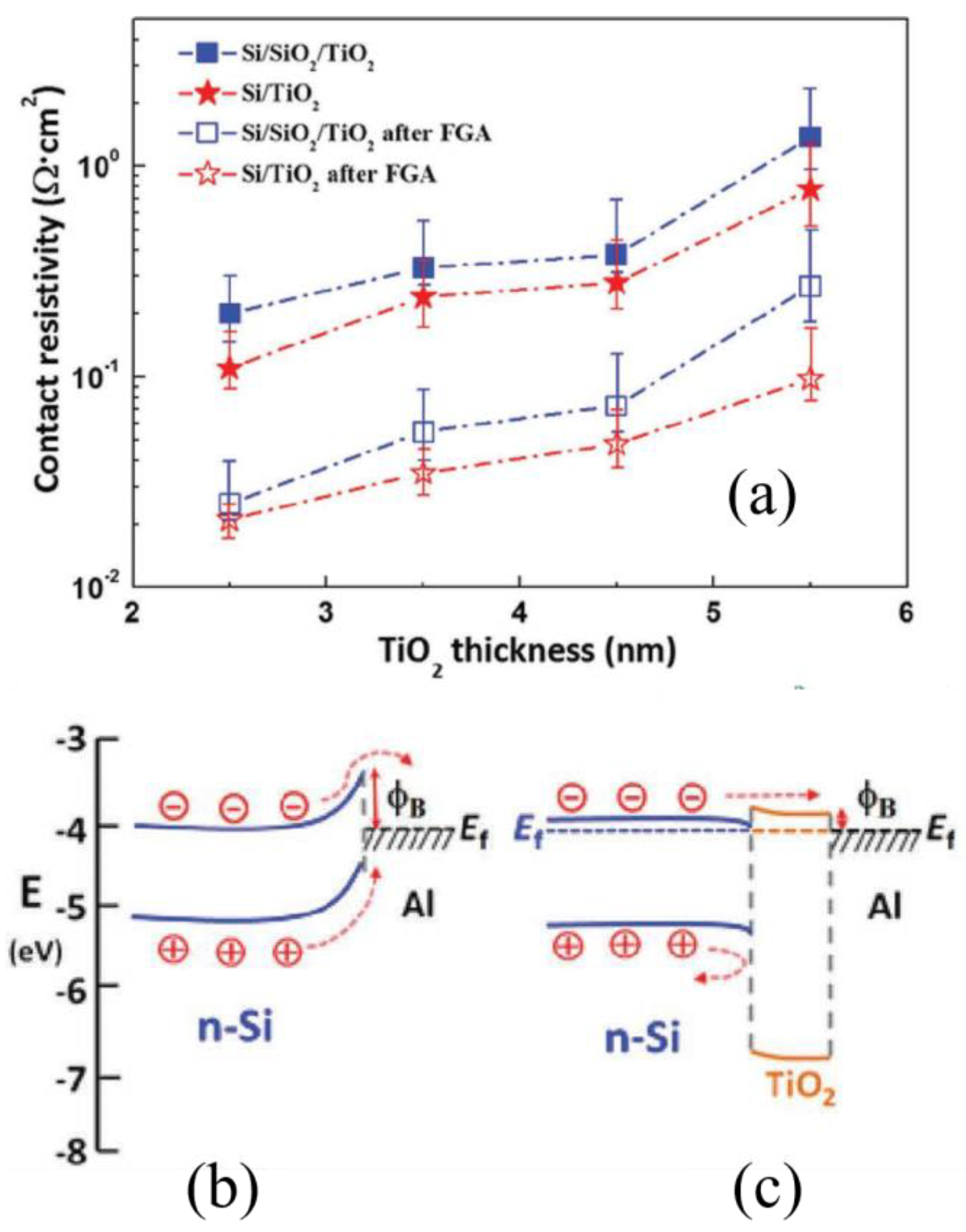
- Matsui, T.; Bivour, M.; Hermle, M.; Sai, H. Atomic-Layer-Deposited TiOx Nanolayers Function as Efficient Hole-Selective Passivating Contacts in Silicon Solar Cells. ACS Appl. Mater. Interfaces 2020, 12, 49777–49785. [Google Scholar] [CrossRef]
- Yang, X.; Bi, Q.; Ali, H.; Davis, K.; Schoenfeld, W.V.; Weber, K. High-Performance TiO2-Based Electron-Selective Contacts for Crystalline Silicon Solar Cells. Adv. Mater. 2016, 28, 5891–5897. [Google Scholar] [CrossRef] [PubMed]
- Lee, C.; Bae, S.; Park, H.; Choi, D.; Song, H.; Lee, H.; Ohshita, Y.; Kim, D.; Kang, Y.; Lee, H.-S. Properties of Thermally Evaporated Titanium Dioxide as an Electron-Selective Contact for Silicon Solar Cells. Energies 2020, 13, 678. [Google Scholar] [CrossRef]
- Avasthi, S.; McClain, W.E.; Man, G.; Kahn, A.; Schwartz, J.; Sturm, J.C. Hole-blocking titanium-oxide/silicon heterojunction and its application to photovoltaics. Appl. Phys. Lett. 2013, 102, 203901. [Google Scholar] [CrossRef]
- Yang, X.; Zheng, P.; Bi, Q.; Weber, K. Silicon heterojunction solar cells with electron selective TiOx contact. Sol. Energy Mater. Sol. Cells 2016, 150, 32–38. [Google Scholar] [CrossRef]
- Jia, H.; Tang, M.; Ge, J. Investigation of Field-Effect Passivation Created by Hydrogen Plasma Etching of Radio Corporation of America Formed Chemical Oxides on Crystalline Silicon Wafers. Phys. Status Solidi A 2021, 218, 2000586. [Google Scholar] [CrossRef]
- Chunduri, S.K.; Schmela, M. Heterojunction Solar Technology 2020 Edition. TaiyangNews, 2 December 2020. [Google Scholar] [CrossRef]
- Yoshikawa, K.; Kawasaki, H.; Yoshida, W.; Irie, T.; Konishi, K.; Nakano, K.; Uto, T.; Adachi, D.; Kanematsu, M.; Uzu, H.; et al. Silicon heterojunction solar cell with interdigitated back contacts for a photoconversion efficiency over 26%. Nat. Energy 2017, 2, 1. [Google Scholar] [CrossRef]
- Green, M.A.; Dunlop, E.D.; Hohl-Ebinger, J.; Yoshita, M.; Kopidakis, N.; Hao, X. Solar cell efficiency tables (version 59). Prog. Photovolt. Res. Appl. 2022, 30, 3–12. [Google Scholar] [CrossRef]
- LONGi Breaks World Record for HJT Solar Cell Efficiency Twice in One Week. Available online: https://www.longi.com/en/news/7469 (accessed on 4 June 2022).
- Duan, W.; Lambertz, A.; Bittkau, K.; Qiu, D.; Qiu, K.; Rau, U.; Ding, K. A route towards high-efficiency silicon heterojunction solar cells. Prog. Photovolt. Res. Appl. 2022, 30, 384–392. [Google Scholar] [CrossRef]
- Ru, X.; Qu, M.; Wang, J.; Ruan, T.; Yang, M.; Peng, F.; Long, W.; Zheng, K.; Yan, H.; Xu, X. 25.11% efficiency silicon heterojunction solar cell with low deposition rate intrinsic amorphous silicon buffer layers. Sol. Energy Mater. Sol. Cells 2020, 215, 110643. [Google Scholar] [CrossRef]
- Qiu, D.; Duan, W.; Lambertz, A.; Bittkau, K.; Steuter, P.; Liu, Y.; Gad, A.; Pomaska, M.; Rau, U.; Ding, K. Front contact optimization for rear-junction SHJ solar cells with ultra-thin n-type nanocrystalline silicon oxide. Sol. Energy Mater. Sol. Cells 2020, 209, 110471. [Google Scholar] [CrossRef]
- Yang, Y.; Liu, W.; Zhang, L.; Huang, S.; Li, X.; Jiang, K.; Li, Z.; Yan, Z.; Lan, S.; Wu, X.; et al. N-type nc-SiOx:H film enables efficient and stable silicon heterojunction solar cells in sodium environment. Mater. Lett. 2022, 309, 131360. [Google Scholar] [CrossRef]
- Liu, W.; Shi, J.; Zhang, L.; Han, A.; Huang, S.; Li, X.; Peng, J.; Yang, Y.; Gao, Y.; Yu, J.; et al. Light-induced activation of boron doping in hydrogenated amorphous silicon for over 25% efficiency silicon solar cells. Nat. Energy 2022, 7, 427–437. [Google Scholar] [CrossRef]
- Dréon, J.; Jeangros, Q.; Cattin, J.; Haschke, J.; Antognini, L.; Ballif, C.; Boccard, M. 23.5%-efficient silicon heterojunction silicon solar cell using molybdenum oxide as hole-selective contact. Nano Energy 2020, 70, 104495. [Google Scholar] [CrossRef]
- Sai, H.; Hsu, H.; Chen, P.; Chen, P.; Matsui, T. Intrinsic amorphous silicon bilayers for effective surface passivation in silicon heterojunction solar cells: A comparative study of interfacial layers. Phys. Status Solidi A 2021, 218, 2000743. [Google Scholar] [CrossRef]
- Krajangsang, T.; Inthisang, S.; Sritharathikhun, J.; Hongsingthong, A.; Limmanee, A.; Kittisontirak, S.; Chinnavornrungsee, P.; Phatthanakun, R.; Sriprapha, K. An intrinsic amorphous silicon oxide and amorphous silicon stack passivation layer for crystalline silicon heterojunction solar cells. Thin Solid Film. 2017, 628, 107. [Google Scholar] [CrossRef]
- Biron, R.; Pahud, C.; Haug, F.; Ballif, C. Origin of the VOC enhancement with a p-doped nc-SiOx:H window layer in nip solar cells. J. Non-Cryst. Solids 2012, 358, 1958–1961. [Google Scholar] [CrossRef]
- Kahn, A. Fermi level, work function and vacuum level. Mater. Horiz. 2016, 3, 7–10. [Google Scholar] [CrossRef]
- Köhler, M.; Pomaska, M.; Zamchiy, A.; Lambertz, A.; Duan, W.; Lentz, F.; Li, S.; Smirnov, V.; Kirchartz, T.; Finger, F.; et al. Optimization of transparent passivating contact for crystalline silicon solar cells. IEEE J. Photovolt. 2020, 10, 46–53. [Google Scholar] [CrossRef]
- Yang, X.; Xu, H.; Liu, W.; Bi, Q.; Xu, L.; Kang, J.; Hedhili, M.N.; Sun, B.; Zhang, X.; De Wolf, S. Atomic layer deposition of vanadium oxide as hole-selective contact for crystalline silicon solar cells. Adv. Electron. Mater. 2020, 6, 2000467. [Google Scholar] [CrossRef]
- Zhong, S.; Dreon, J.; Jeangros, Q.; Aydin, E.; De Wolf, S.; Fu, F.; Boccard, M.; Ballif, C. Mitigating plasmonic absorption losses at rear electrodes in high-efficiency silicon solar cells using dopant-free contact stacks. Adv. Funct. Mater. 2019, 30, 1907840. [Google Scholar] [CrossRef]


| Features | Cleaning | PCE [%] | FF [%] | VOC [mV]/ δ [µm] | JSC [mA/cm2]/ Area [cm2] | Reference/ Year |
|---|---|---|---|---|---|---|
| SHJ-IBC, a-Si:H contact | - | 26.7 | 84.9 | 738/ 165 | 42.65/ 79 | [140,141]/ 2017 |
| Microcrystalline layer, new i layer | - | 26.3 | 86.59 | 750.2/ - | 40.49/ 274.3 | [142]/ 2022 |
| SHJ | - | 25.1 | 83.5 | 738/ 160 | 40.8/ 151.9 | [8]/ 2015 |
| a-Si:H(i1)/a-Si:H(i2)/a-Si:H(p) at backside | Ozone | 24.51 | 83.61 | 741.8/ 180 | 39.52/ 244.53 | [143]/ 2022 |
| Both sides i1 + i2 a-Si:H a-Si:H(n)/nc-SiOx:H(n) as front ESL | - | 25.11 | 84.98 | 747/ 150 | 39.55/ 244.45 | [144]/ 2020 |
| nc-SiOx:H(n)/nc-Si:H(n) as front ESL | Ozone | 23.1 | 80.7 | 739/ 170 | 39.0/ 244 | [145]/ 2020 |
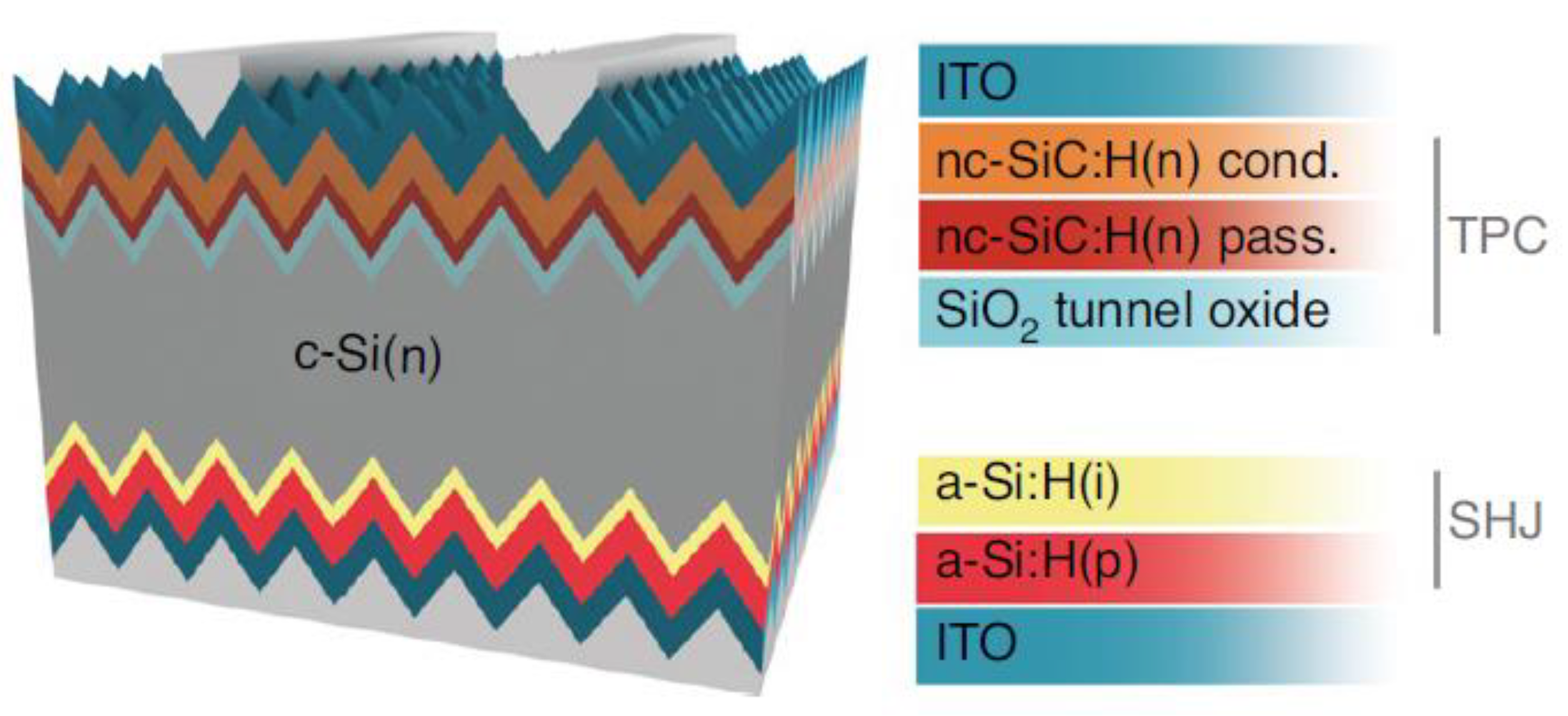
| Stacked nc-SiC:H(n) as front ESL, SiO2 tunnel oxide at front side | RCA | 23.99 | 80.9 | 725/ 170 | 40.87/ 3.487 | [97]/ 2021 |
| (Seed layer) nc-Si:H(n)/nc-SiOx:H(n) as front ESL | RCA | 24.09 | 84.5 | 744/ 140 | 38.3/ 243.36 | [146]/ 2022 |
| Enhanced doping efficiency of B-Si4 | RCA | 25.18 | 85.42 | 749.1/ 160 | 39.36/ 244.63 | [147]/ 2022 |
| MoOx as front HSL, a-Si:H(n)/µc-Si:H(n) as back ESL | - | 23.5 | 81.8 | 734/ 180 | 39.2/ 3.972 | [148]/ 2020 |
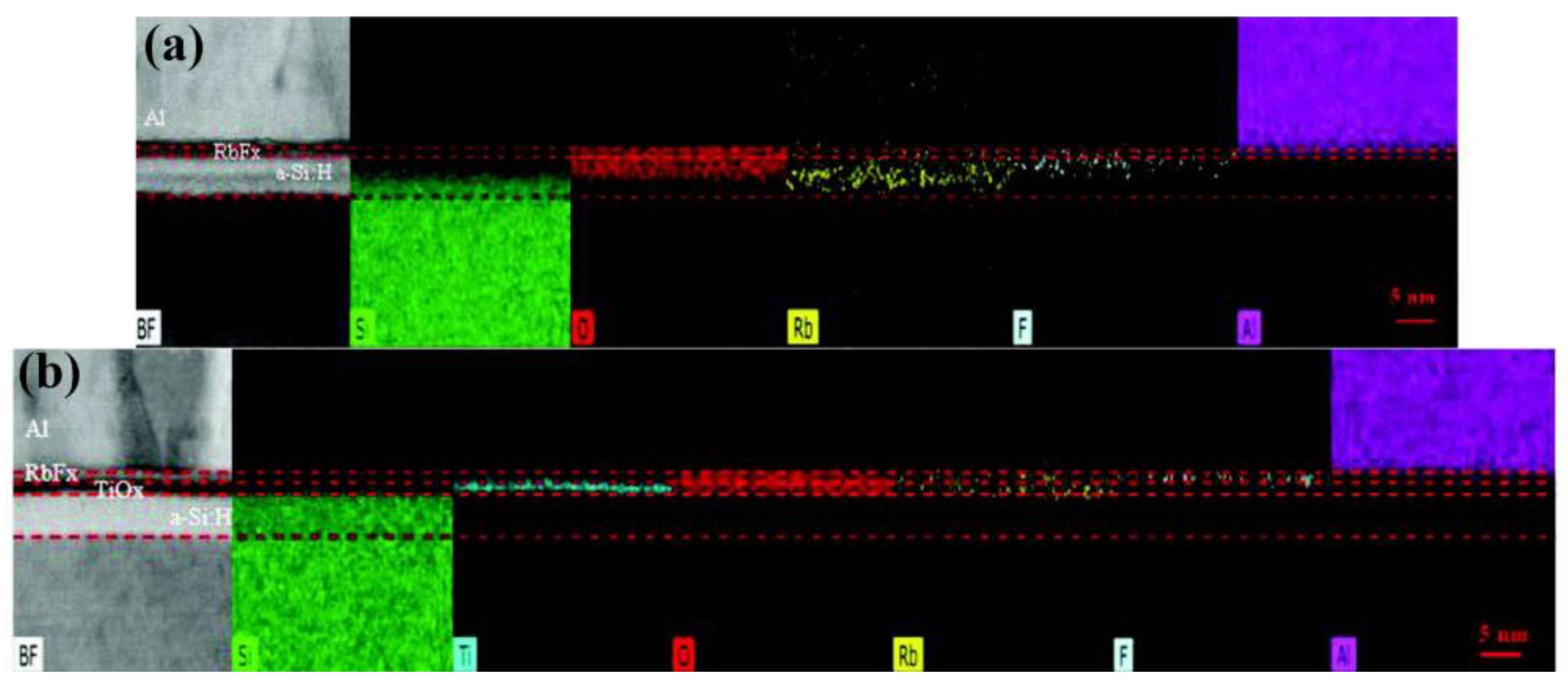
| MoOx as back HSL a-Si:H(i)/TiOx/RbFx/Al as front ESL | RCA | 22.9 | 79.6 | 709/ 145 | 40.5/ 2.56 | [132]/ 2022 |
| MoOx as front HSL a-Si:H(i)/TiOx/LiFx/Al as back ESL | 20.7 | 76.2 | 706 250 | 38.4 4 | [131] 2018 |
Disclaimer/Publisher’s Note: The statements, opinions and data contained in all publications are solely those of the individual author(s) and contributor(s) and not of MDPI and/or the editor(s). MDPI and/or the editor(s) disclaim responsibility for any injury to people or property resulting from any ideas, methods, instructions or products referred to in the content. |
© 2023 by the authors. Licensee MDPI, Basel, Switzerland. This article is an open access article distributed under the terms and conditions of the Creative Commons Attribution (CC BY) license (https://creativecommons.org/licenses/by/4.0/).
Share and Cite
Shi, C.; Shi, J.; Guan, Z.; Ge, J. Surface Cleaning and Passivation Technologies for the Fabrication of High-Efficiency Silicon Heterojunction Solar Cells. Materials 2023, 16, 3144. https://doi.org/10.3390/ma16083144
Shi C, Shi J, Guan Z, Ge J. Surface Cleaning and Passivation Technologies for the Fabrication of High-Efficiency Silicon Heterojunction Solar Cells. Materials. 2023; 16(8):3144. https://doi.org/10.3390/ma16083144
Chicago/Turabian StyleShi, Cuihua, Jiajian Shi, Zisheng Guan, and Jia Ge. 2023. "Surface Cleaning and Passivation Technologies for the Fabrication of High-Efficiency Silicon Heterojunction Solar Cells" Materials 16, no. 8: 3144. https://doi.org/10.3390/ma16083144