Article

In Situ Grown 1D/2D Structure of Dy3Si2C2 on SiCw for Enhanced Electromagnetic Wave Absorption

1
School of Materials Science and Chemical Engineering, Ningbo University, Ningbo 315211, China
2
Engineering Laboratory of Advanced Energy Materials, Ningbo Institute of Materials Technology and Engineering, Chinese Academy of Sciences, Ningbo 315201, China
3
National Key Laboratory of Science and Technology on High-Strength Structural Materials, Central South University, Changsha 410083, China
4
Hunan Key Laboratory of Applied Environmental Photocatalysis, Changsha University, Changsha 410022, China
*
Authors to whom correspondence should be addressed.
Materials 2023, 16(9), 3455; https://doi.org/10.3390/ma16093455
Submission received: 20 March 2023 / Revised: 21 April 2023 / Accepted: 24 April 2023 / Published: 28 April 2023
(This article belongs to the Special Issue Innovative Applications of Materials to Industrial Design)

Abstract

:
To improve electromagnetic wave (EMW) absorption performance, a novel nano-laminated Dy3Si2C2 coating was successfully in situ coated on the surface of SiC whisker (SiCw/Dy3Si2C2) using a molten salt approach. A labyrinthine three-dimensional (3D) net was constructed by the one-dimensional (1D) SiCw coated with the two-dimensional (2D) Dy3Si2C2 layer with a thickness of ~100 nm, which significantly improved the EMW absorption properties of SiCw. Compared to pure SiCw with the minimum reflection loss (RLmin) value of −10.64 dB and the effective absorption bandwidth (EAB) of 1.04 GHz for the sample with a thickness of 4.5 mm, SiCw/Dy3Si2C2 showed a significantly better EMW absorption performance with RLmin of −32.09 dB and wider EAB of 3.76 GHz for thinner samples with a thickness of 1.76 mm. The enhancement of the EMW absorption performance could be ascribed to the improvement of impedance matching, enhanced conductance loss, interfacial polarization as well as multiple scattering. The SiCw/Dy3Si2C2 can be a candidate for EMW absorber applications due to its excellent EMW absorption performance and wide EAB for relatively thin samples, light weight, as well as potential oxidation and corrosion resistance at high temperatures.

1. Introduction

Electromagnetic wave (EMW) radiation pollution seriously endangers human health, as a consequence of the widespread applications of the high frequency electronic devices [1,2,3,4,5]. In recent years, numerous EMW absorption materials have been developed to solve these problems [6,7], including carbon-based materials [8,9], magnetic metal materials [10,11,12], ferrite and its composites [13,14,15], and polymer matrix composites [16,17,18]. However, the poor oxidation resistance of carbon-based materials and polymer matrix composites at high temperatures has impeded their applications, despite their excellent EMW absorption properties [19]. Magnetic materials also cannot be used at high temperatures due to the demagnetization [20]. Furthermore, a relatively high density of ferrite materials also hinders their applications in some special fields, such as aerospace. Therefore, the development of high performance EMW absorption materials with high absorption capability, broad effective absorption bandwidth (EAB), low density as well as small thickness, and excellent oxidation resistance at high temperatures is a critical challenge in this field to minimize EMW radiation pollution.
SiC has been considered a promising candidate for EMW absorbers because it has excellent dielectric properties, high temperature stability, as well as outstanding oxidation and corrosion resistance [21,22]. Most of the works on SiC-based EMW absorption materials have been focused on the SiC nanoparticles (SiCNP), SiC fibers (SiCf), SiC nanowires (SiCNWs), and SiC whiskers (SiCw) [23,24,25,26,27,28]. Among all of them, one-dimensional (1D) SiCw or SiCNWs have drawn the most significant attention, since they have large aspect ratio, which is good for dissipating current by providing long transport paths, resulting in a strong conduction loss [29]. Furthermore, a three-dimensional (3D) network can be easily constructed, which is beneficial to improving the EMW absorption performance [27,30]. However, the EMW absorption properties of pure SiCw cannot meet the strict requirements of a strong absorption and a broad EAB because of the poor impedance matching and single EMW loss mechanism [31,32,33]. Therefore, many research works have been conducted to improve the EMW absorption properties of SiCw, including elemental doping, surface modification, and fabrication of SiCw-based composites [34,35]. For example, Kuang et al. reported that the electrical conductivity of SiCw was significantly enhanced by Al-doping. The lowest reflection loss (RL) value was −25.4 dB, and the EAB was 2 GHz when the Al/Si ratio was 0.03/0.97 [29]. In particular, surface modification of SiCw has been demonstrated to be an efficient and feasible method for improving the EMW absorption [27,31,36].
Rare earth silicide carbides (RE3Si2C2, where RE is a rare earth element) are a new group of ternary layered structure materials, which are similar to MAX phases (where M is an early transition metal, A is an A-group element, and X is either C or N) [37,38]. RE3Si2C2 has been successfully used as the joining layer material and/or sintering additive for SiC-based ceramics and composites due to its ability to form a liquid phase by the eutectic reaction with SiC [39,40,41,42,43,44,45,46]. Furthermore, the addition of a second phase can significantly promote the EMW absorption properties of the resulting composites [47,48]. Our previous work indicated that the EMW absorption properties of SiCf can be significantly improved by the incorporation of Y3Si2C2 coating on the SiCf surface [3]. The minimum RL of SiCf/Y3Si2C2 was -16.98 dB at a thin thickness of 2.19 mm. Furthermore, compared to the EAB of 1.92 GHz at the thickness of 3.38 mm for pure SiC fiber, SiCf/Y3Si2C2 shows significantly wider optimal EAB of 5.44 GHz at a much thinner thickness of 2.64 mm [3]. SiCw whiskers have a larger aspect ratio compared to the chopped SiC fibers. It is relatively easy to form a 3D net, which is beneficial for increasing the heterogeneous interfaces and multiple reflections and scattering. Therefore, it is expected that SiCw/Dy3Si2C2 could show even better EMW absorption properties when compared to SiCf/Y3Si2C2.
In this work, the two-dimensional (2D) Dy3Si2C2 coating is formed on the one-dimensional (1D) SiCw surface by the molten salt method to improve the EMW absorption properties. Combining Dy3Si2C2 with SiCw not only effectively improved the impedance matching but also provided a large number of heterogeneous interfaces as well as enhanced interface polarization loss. At the same time, the stacking effect of one-dimensional structures builds an efficient three-dimensional conductive network that enhances resistance loss. Furthermore, the two-dimensional layered structure of Dy3Si2C2 can improve multiple reflections, which is beneficial to improving the EMW absorption properties. Microstructure, phase composition, dielectric, and EMW absorption properties of the as-obtained SiCw/Dy3Si2C2 coated whiskers were investigated. The possible EMW absorption mechanism of SiCw/Dy3Si2C2 was summarized. EMW absorption properties of the as-obtained SiCw/Dy3Si2C2 were compared to the previously reported materials.

2. Experimental Procedure

2.1. Materials and Experiments

DyH2 powder with a purity of 99.9% and a mean particle size of ~75 μm was purchased from Institute of Hunan rare earth metal materials Co., Ltd., Changsha, China. SiC whiskers (Union Materials Co., Daegu, Republic of Korea) with a diameter of 0.4–0.9 μm and a length of 6–120 μm; NaCl; and KCl powders (purity: 99.5%, mean particle size: 75 µm; Sinopharm Chemical Reagent Co., Ltd., Shanghai, China) were used as the raw materials.
The DyH2, SiCw, NaCl, and KCl powders with the molar ratio of DyH2: SiCw =1:4 and NaCl:KCl = 1:1 were mixed for 30 min in an Ar atmosphere in a home-made glove box. The mixed DyH2, SiCw, NaCl, and KCl powders were heated to a target temperature of 1000 °C in the molten salt furnace. The holding time was set 5 h. The heating and cooling rate was 5 °C/min. The as-obtained samples were washed and filtered using deionized water several times. The in situ coated SiCw/Dy3Si2C2 powder can be obtained after drying 12 h at 60 °C in a vacuum oven.

2.2. Characterizations

The phase compositions of the as-obtained SiCw/Dy3Si2C2 were detected using an X-ray diffractometer (XRD: D8 Advance, Bruker AXS, Karlsruhe, Germany) using Cu Kα radiation (λ = 1.5406 Å). The operating current and voltage were 40 mA and 40 kV, respectively. The step scan and step time was 0.02° 2θ and 0.2 s, respectively. The microstructure of the SiCw/Dy3Si2C2 powders was observed using a scanning electron microscope (SEM, 8230, Hitachi, Tokyo, Japan). The microstructure and phase compositions of the Dy3Si2C2 coating were further investigated using a transmission electron microscope (TEM, Talos F200X, Thermo Fisher Scientific, Waltham, MA, USA) equipped with an energy dispersive spectroscopy (EDS) system. The samples for TEM observations were prepared using the focused ion beam (FIB, Auriga, Carl Zeiss, Jena, Germany) technique. The complex permittivity and complex permeability were measured at a frequency range from 2 to 18 GHz using a Network Analyzer of Agilent N5230A. In order to measure the complex permittivity and complex permeability, SiCw/Dy3Si2C2 powder was mixed with 50 wt.% paraffin with a size of an inner and outer diameter of 3 and 7 mm as well as a thickness of 2 mm, respectively. For the sake of comparison, the electromagnetic properties of the pure SiC whiskers were detected using the same method.

3. Results and Discussion

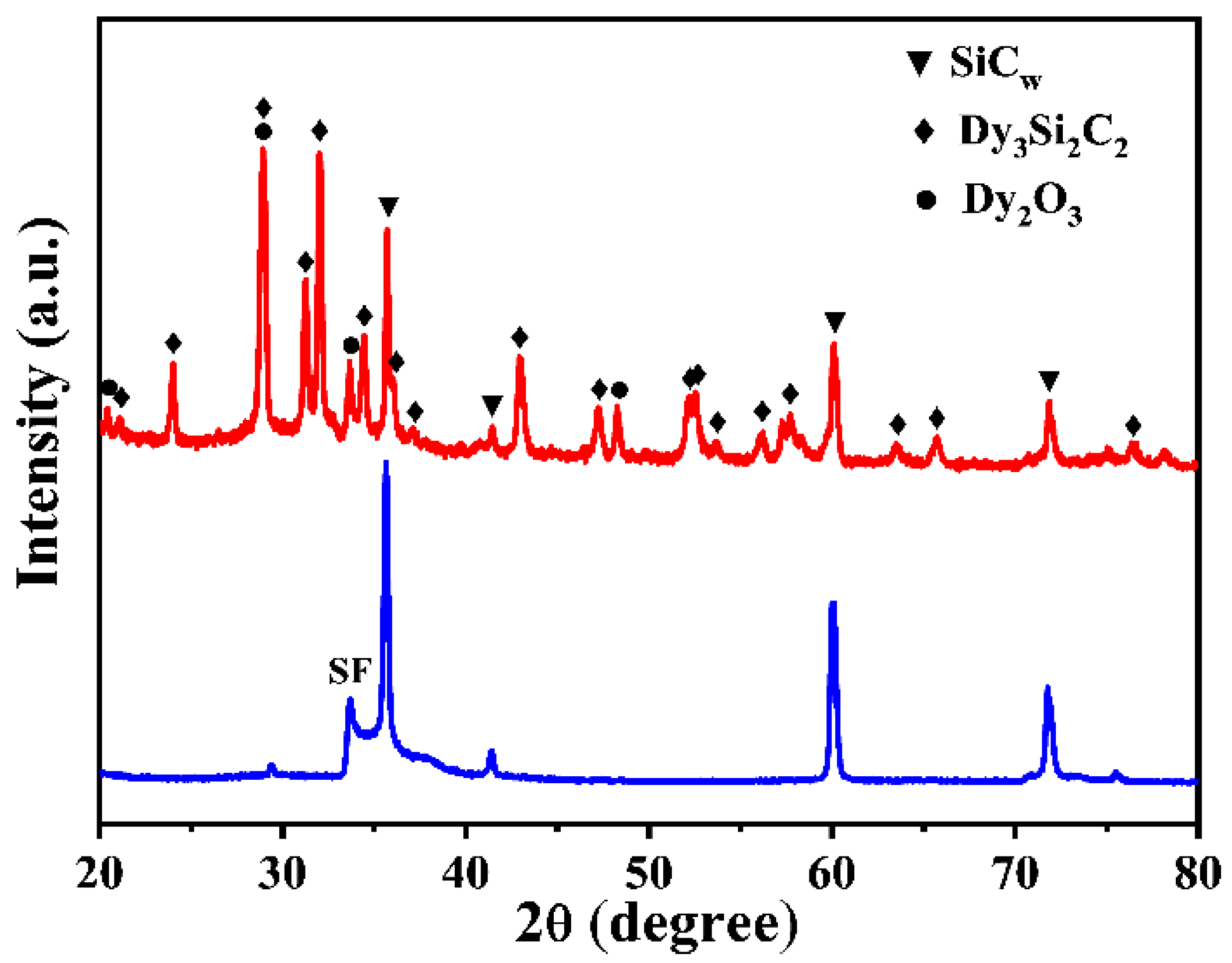
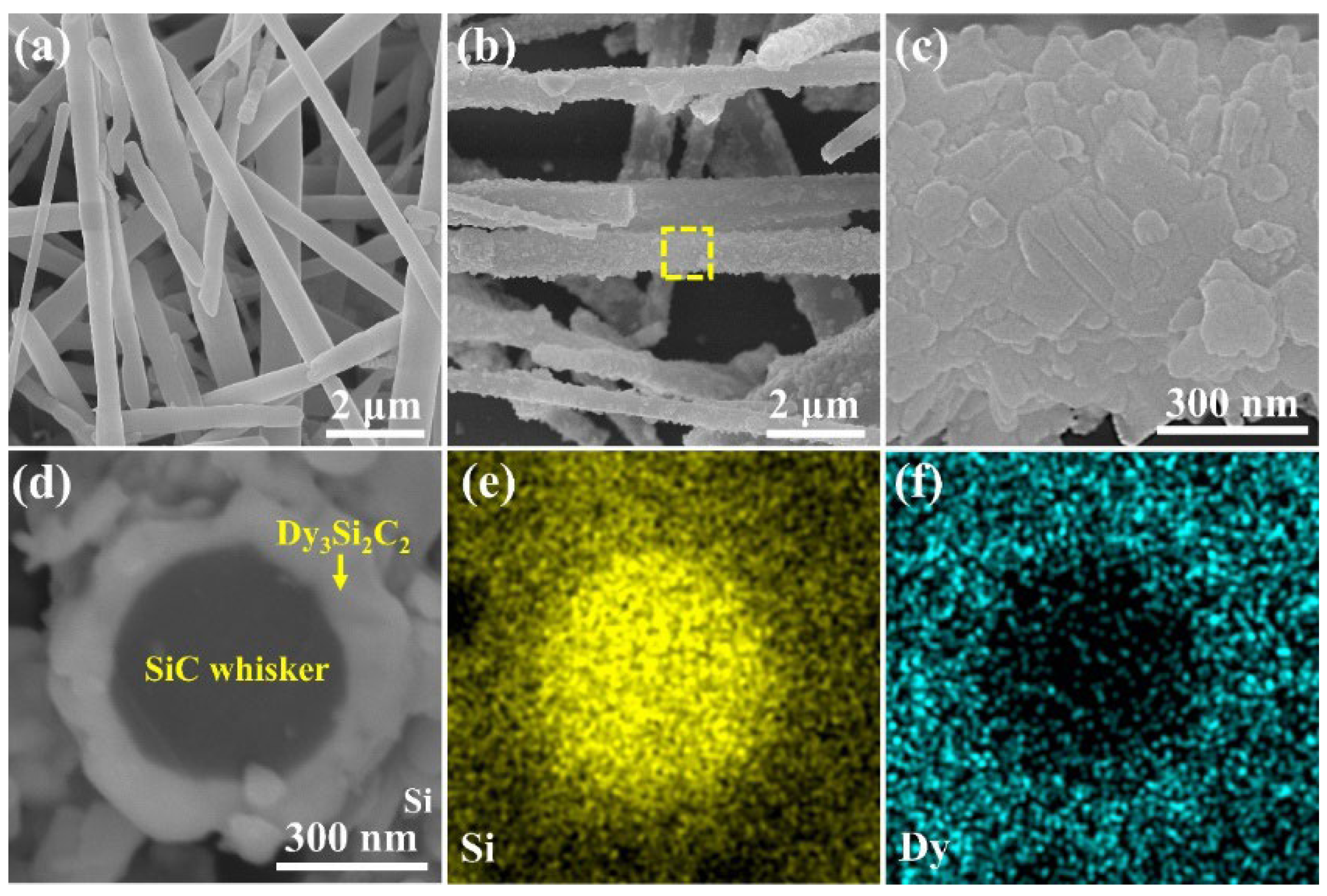
3.1. Microstructure and Phase Composition of SiCw/Dy3Si2C2

Figure 1 presents the XRD patterns of the pure SiC whiskers and the as-obtained SiCw/Dy3Si2C2 whiskers.
The XRD pattern of pure SiC whiskers indicated that they are formed by the 3C-SiC phase (JCPDS No. 75-0254). A small peak at approximately 33.5° corresponds to the stacking faults, which spontaneously formed during the growing process of SiC whiskers. The XRD pattern of the SiCw/Dy3Si2C2 powder revealed that besides SiCw, it also contained characteristic peaks of Dy3Si2C2 (JCPDS No. 97-005-1299) along with some impurities of Dy2O3 (JCPDS No. 97-018-5606). This confirmed that the Dy3Si2C2 modification of SiC whiskers was successfully obtained.
Figure 2 shows the SEM images of both SiCw and SiCw/Dy3Si2C2 whiskers.
The diameter of the pure SiC whiskers was ~500 nm. A dense 2D structure Dy3Si2C2 coating with a structure of randomly oriented nano-laminated sheets was in situ coated on the surface of SiC whiskers (Figure 2b,c). The thickness of Dy3Si2C2 coating was around 100 nm, as shown in the SEM image of the fracture surface of the SiCw/Dy3Si2C2 whisker (Figure 2d). The corresponding elemental distribution of Si and Dy indicated that most of the Dy3Si2C2 was homogenously coated on the surface of SiC whisker (Figure 2e,f).
To further confirm the microstructure and phase composition of the Dy3Si2C2 coating, semi-quantitative EDS and high-resolution transmission electron microscope (HR-TEM) analysis along with selected-area electron diffraction (SAED) were performed. Figure 3 presents a high-angle annular dark-field (HAADF) image of the as-synthesized SiCw/Dy3Si2C2 and the corresponding Dy, Si, C, and O elemental distributions, respectively.
The semiquantitative EDS analysis results of areas 1–3 are shown in Table 1, suggesting the presence of SiC, Dy3Si2C2, and/or Dy2O3.
Furthermore, the HR-TEM image of the interface between SiCw and Dy3Si2C2 coating is shown in Figure 3f. The lattice fringe spacing was 0.2878 nm, which can be assigned to the (041) planes of Dy3Si2C2. Therefore, taking into account all the results obtained by XRD, EDS, and HR-TEM analysis, it can be concluded that a dense ~100 nm Dy3Si2C2 coating was successfully fabricated on the surface of SiCw using the molten salt approach.
The formation process of the Dy3Si2C2 coating using the molten salt approach is similar to the formation mechanism of Y3Si2C2 and Pr3Si2C2 powders [45,48]. First, DyH2 decomposed to Dy and released H2 [49]. The Dy element diffused to the surface of SiC whiskers via the liquid molten salt, and then the Dy3Si2C2 coating was formed. The main reactions can be summarized as follow:
DyH 2 Dy + H 2
3 Dy + 2 SiC Dy 3 Si 2 C 2
On the other hand, the potential formation barrier of the Dy3Si2C2 could decline because the surface energy of both DyH2 and SiCw could be remarkably promoted by polarization effect of the molten salt [50,51]. In addition, the diffusion rate of the Dy, Si, and C atoms can be obviously promoted in the liquid molten salt reaction medium. Therefore, the Dy3Si2C2 coating can be in situ formed on the surface of SiC whiskers at a relatively low temperature (1000 °C) and adhered well to the surface of SiCw.

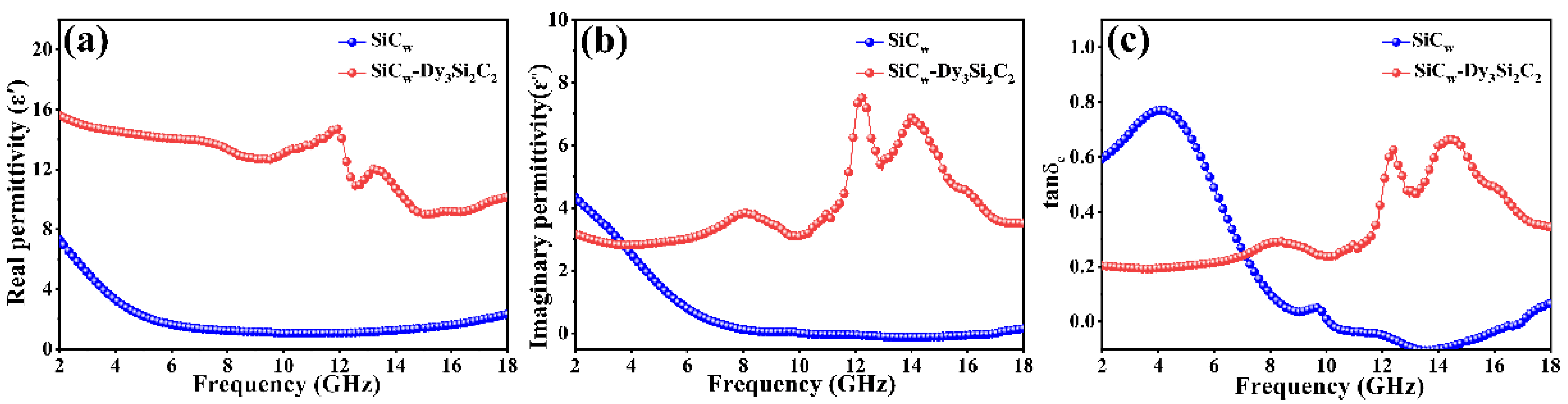
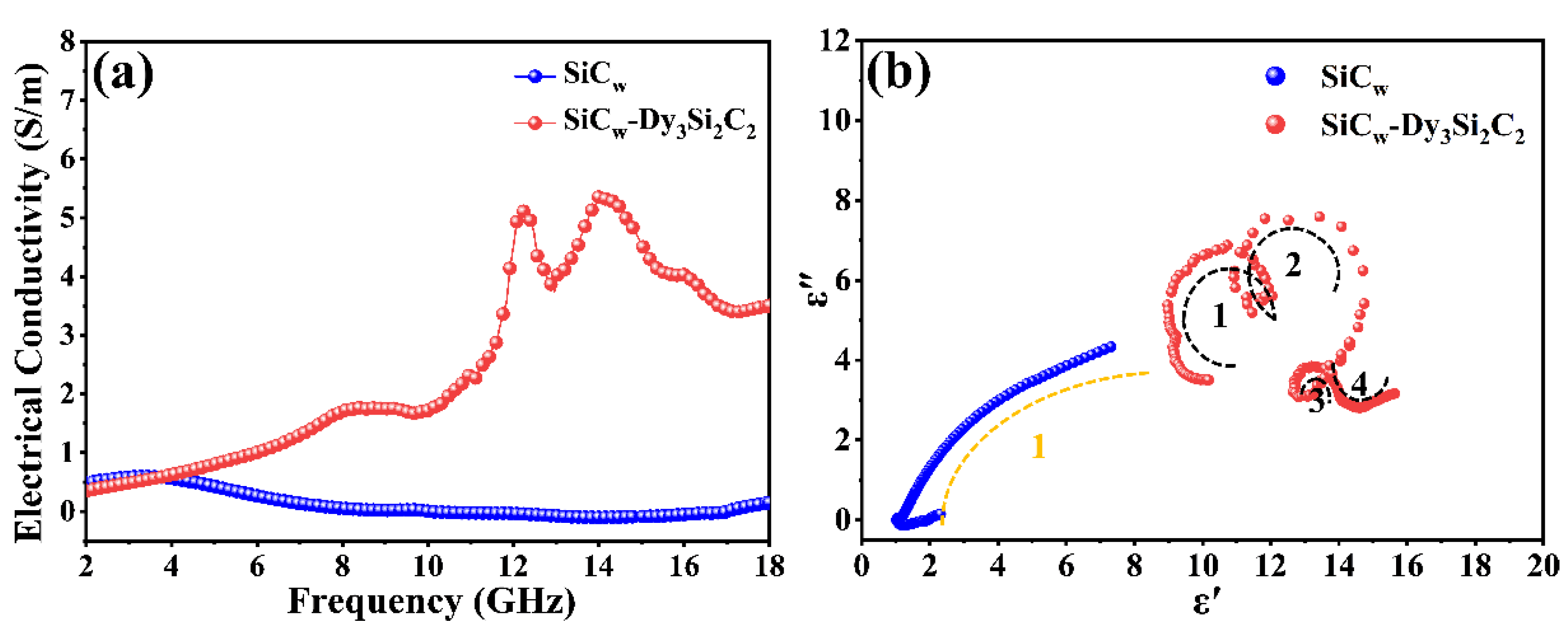
3.2. Dielectric Properties of SiCw/Dy3Si2C2

The EMW absorption property of materials is mainly confirmed by their complex permittivity and permeability. Meanwhile, good impedance matching between absorbing materials and free space can make EMW incident into materials with less reflection. While SiCw and SiCw/Dy3Si2C2 are nonmagnetic materials, the real (μ′) and imaginary (μ″) parts of the complex permeability is around 1 and 0, respectively (not shown here). Therefore, the EMW absorption capability of SiCw and SiCw/Dy3Si2C2 is highly dependent on their complex permittivity. The real (ε′) and imaginary (ε″) parts of complex permittivity of the pure SiCw and SiCw/Dy3Si2C2 whiskers are shown in Figure 4.
Most of the real (ε′) and imaginary (ε″) parts of the complex permittivity of SiCw/Dy3Si2C2 were higher than that of pure SiCw, indicating that the Dy3Si2C2 coating could promote the dielectric properties of SiCw.
According to the Debye theory, ε′ and ε″ can be calculated by the following equations [52]:
ε = ε + ε s ε / 1 + ω τ 2
ε = ε s ε / 1 + ω τ 2 + δ a c / ω ε 0 = ε p + ε c
where ε0, εs, and ε represent free space dielectric constant, the permittivity in static state, and light frequency, respectively. ω and τ are angular frequency and polarization relaxation time, respectively. σ is electric conductivity. εp″ and εc″ correspond to the contributions to ε″ from polarization loss and conductance loss, which are associated with σ. Generally, the real part of the permittivity signifies the storage capability of the dielectric energy, while the imaginary part of the permittivity stands for the loss of dielectric energy [53]. Thus, the improvement of ε′ can be ascribed to the interfacial polarization caused by the improved heterogeneous interfaces in SiCw/Dy3Si2C2 whiskers, which were generated by the incorporation of nano-laminated (2D) Dy3Si2C2 coating on the surface of SiCw. The enhancement of ε″ was mainly decided by the increasing of the electrical conductivity ( σ ), where σ can be confirmed by the follow equation [54]:
σ = 2 π ε 0 ε ε
where ε0 represents the permittivity in a vacuum.
The electrical conductivity of SiCw/Dy3Si2C2 was higher than that of pure SiCw, as shown in Figure 5a.
This can be mainly attributed to the metallic conductivity characteristic of the 2D structural Dy3Si2C2 coating, as the coating formed a net structure, increasing the transmission channels of carriers [55]. In addition, both ε′ and ε″ of SiCw/Dy3Si2C2 showed a fluctuation corresponding to the resonance, while this was not observed for the pure SiCw. The permittivity of the SiCw/Dy3Si2C2 whiskers showed typical nonlinear resonant characteristics, indicating the existence of polarization and relaxation behavior, which implied better dielectric loss performance in the corresponding frequency range. The Cole–Cole semicircle was used to investigate the relaxation polarization process. According to the Debye theory, the relationship between ε′ and ε″ can be expressed by Equation (6) [56]:
ε ε s + ε / 2 2 + ε = ε s ε / 2
The Cole–Cole curves of pure SiCw and SiCw/Dy3Si2C2 are shown in Figure 5b. Each Deby relaxation process is manifested by one Cole-Cloe semicircle [55,56]. There was only one Cole–Cole semicircle observed in pure SiCw, indicating one relaxation process, while four semicircles were observed in SiCw/Dy3Si2C2, confirming the improvement of dielectric loss capacity in SiCw/Dy3Si2C2. The improvement of the relaxation process of SiCw/Dy3Si2C2 was mainly caused by the significantly increased interface relaxation, which resulted from the improved number of heterogeneous interfaces in SiCw/Dy3Si2C2.

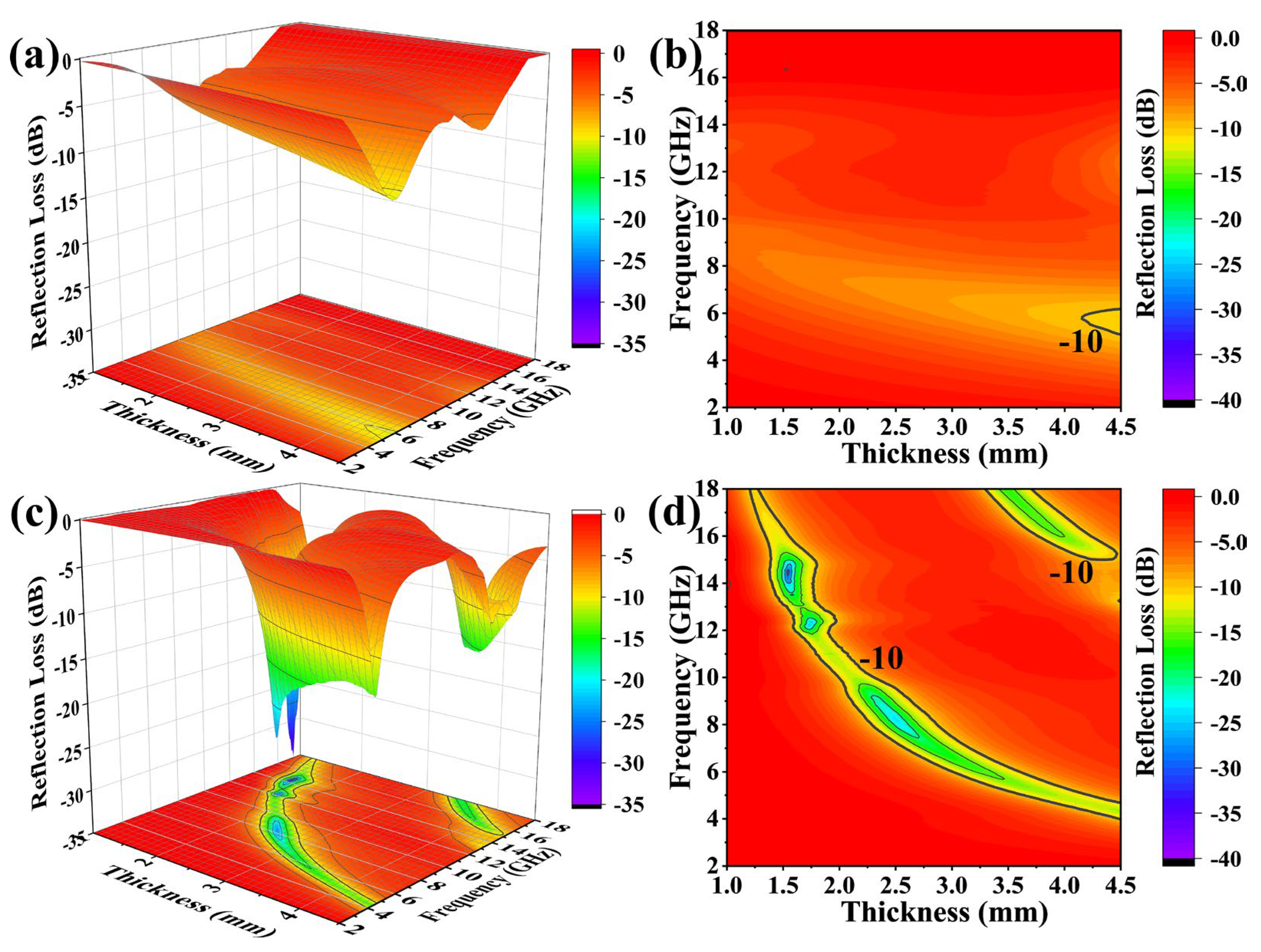
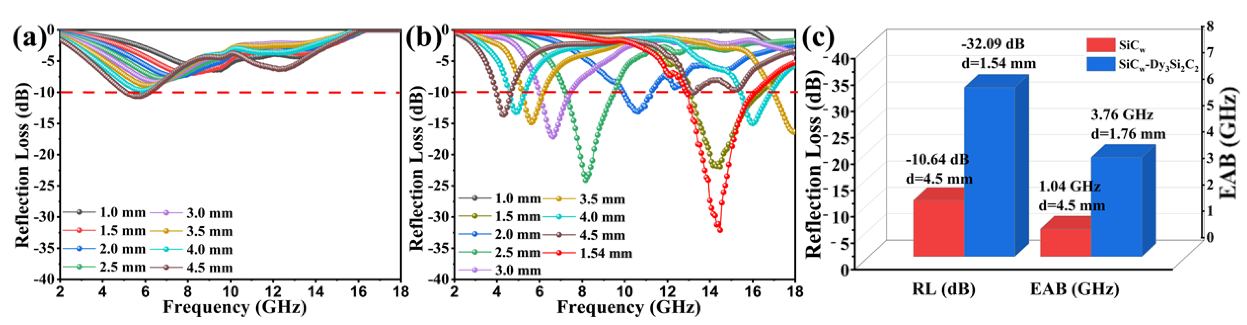
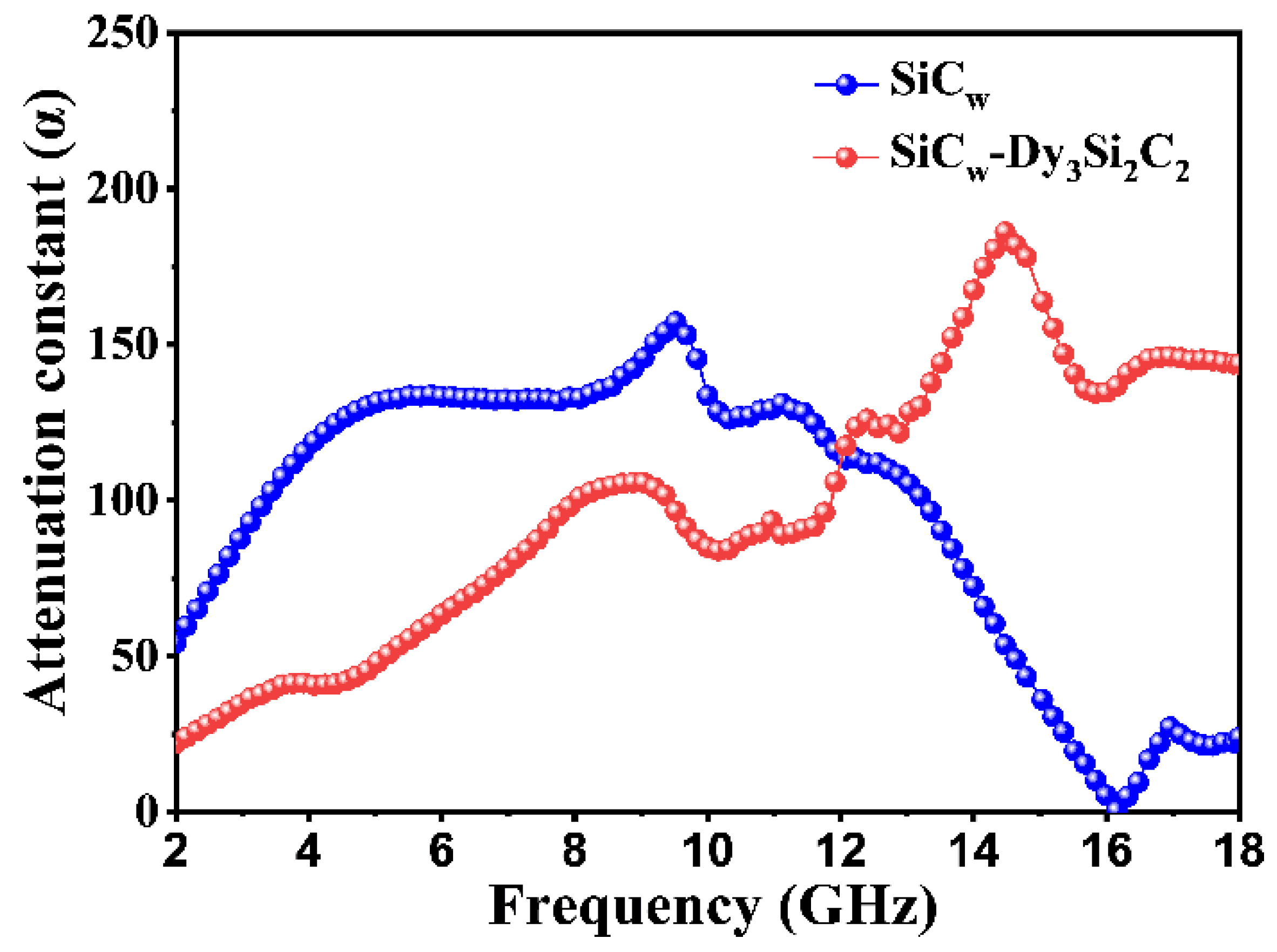
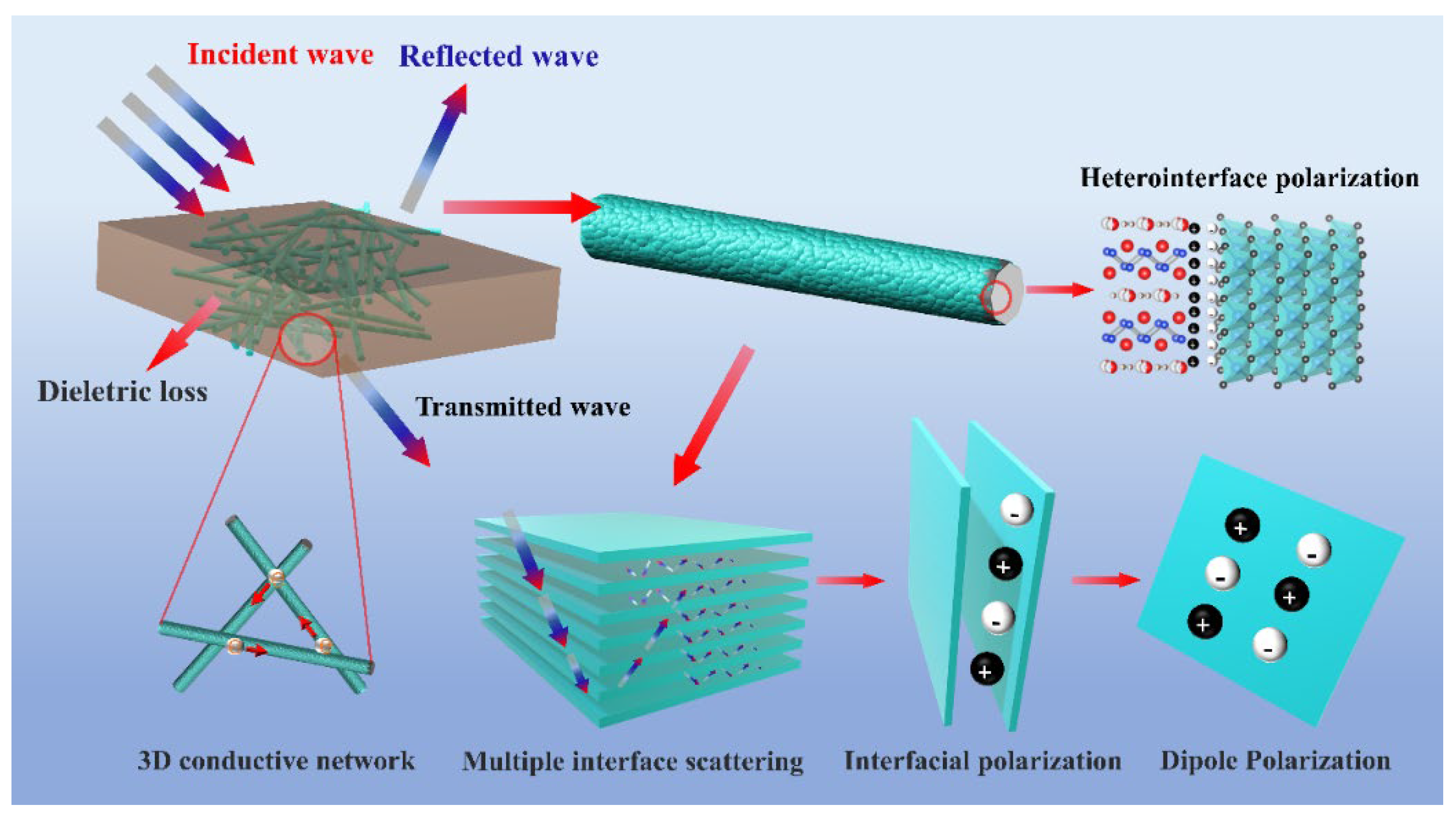
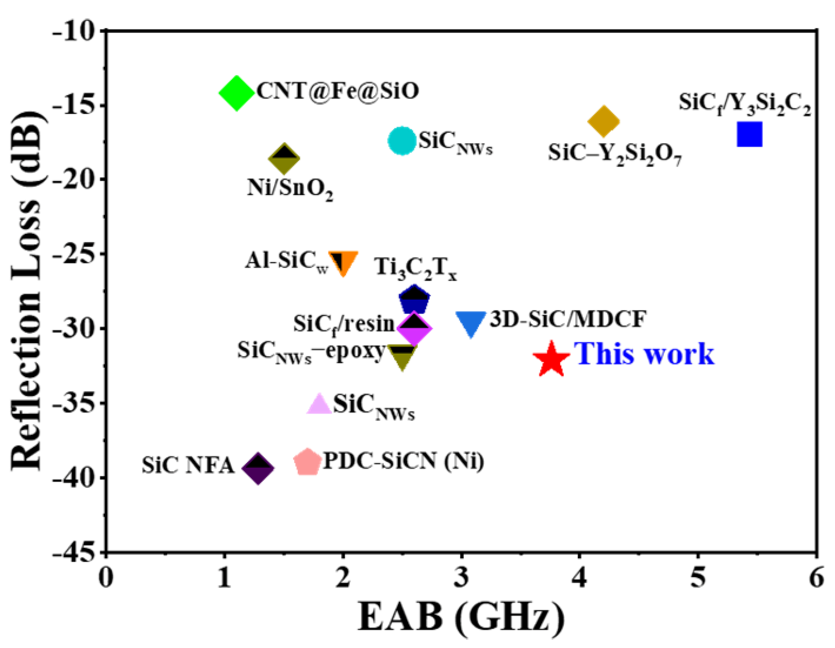
3.3. Electromagnetic Wave Absorption Performance

Reflection loss (RL) and effective absorption bandwidth (EAB, the corresponding frequency range of RL < −10 dB, which presents more than 90% EMW energy absorbed) are usually used to evaluate the EMW absorption performance of materials. According to the transmission line theory, the RL values of SiCw and SiCw/Dy3Si2C2 can be calculated by the following equations [57,58,59]:
R L d B = 20 log Z i n Z 0 / Z i n + Z 0
Z i n = Z 0 μ r / ε r tanh j 2 π f d / c μ r ε r
Z 0 = μ r / ε r
where Z0 and Zin is space free impedance and input impedance, respectively. c, d, and f are speed of light, thickness, and frequency, respectively. μr = μ′″ and εr = ε′ − ″ represent the complex permeability and permittivity of material.
Figure 6 shows the 3D and 2D plots of RL values at the frequency range of 2 to 18 GHz at different thicknesses of the SiCw and SiCw/Dy3Si2C2 samples.
The minimum RL (RLmin) value of the pure SiCw is −10.64 dB at the frequency of 5.52 GHz with the 4.5 mm sample thickness. After coating of SiCw with 2D Dy3Si2C2 sheets, the RLmin value was improved to −32.09 dB at the frequency of 14.48 GHz for the 1.54 mm sample thickness. For convenience of comparison, the selected theoretical calculated RL of pure SiCw and SiCw/Dy3Si2C2 with different thicknesses in the frequency range of 2 to 18 GHz is shown in Figure 7a,b.
It is obvious that the EAB of SiCw/Dy3Si2C2 is much wider than that of SiCw for the samples with the thickness range of 1 to 4.5 mm at the frequency ranging from 2 to 18 GHz. The widest EAB can be as high as 3.76 GHz for thin SiCw/Dy3Si2C2 samples with the thickness of 1.76 mm (Figure 7c). However, the widest EAB of pure SiCw is only 1.04 GHz for the sample with a thickness of 4.5 mm (Figure 7c). This indicates that the Dy3Si2C2 coating can significantly improve the EMW absorption properties of SiCw.
In order to reveal the intrinsic reason for the improved EMW absorption performance for SiCw/Dy3Si2C2, the impedance match (Z) as well as the attenuation constant (α) were calculated. Z was confirmed by the following equation [60]:
Z = Z i n / Z 0 = μ r / ε r tanh j 2 π f d / c μ r ε r
A favorable impedance match is the basic requirement to obtain an excellent EMW absorption performance, which ensures the EMW can enter materials instead of being reflected [61,62,63,64]. According to Equation (10), when the input impedance (Zin) is infinitely close to the air impedance (Z0), the ideal impedance matching can be obtained. Figure 8a,b presents the calculated Z values of the pure SiCw and SiCw/Dy3Si2C2 samples with the thickness of 1–4.5 mm at the frequency ranging from 2 to 18 GHz.
The frequency range with good impedance match (Z-value is close to 1) of SiCw/Dy3Si2C2 was much larger than that of pure SiCw, which indicates that the impedance match of the SiCw was well improved by the Dy3Si2C2 coating. Therefore, the EMW can enter the SiCw/Dy3Si2C2 sample, while most of the EMW was reflected in the case of pure SiCw due to the poor impedance matching.
Furthermore, to evaluate the attenuation ability of EMW energy of the samples, the α (Figure 9) was evaluated by the following formula [53]:
α = 2 π f c μ ε μ ε + μ ε μ μ 2 + μ ε μ ε 2
A larger value of α implies a stronger attenuation ability [65]. The sole high dielectric loss of SiCw at a low frequency resulted in a high attenuation constant, which meant that most of the EMW was reflected. This is in good agreement with the poor impedance matching of the SiCw sample. On the other hand, the introduction of the nano-laminated (2D) Dy3Si2C2 coating significantly improved the impedance match as well as the attenuation ability of the SiCw/Dy3Si2C2. As a result, the EMW absorption property was significantly improved.
The possible EMW absorption mechanism of SiCw/Dy3Si2C2 is illustrated in Figure 10.
Firstly, the favorable impedance matching suggests that the majority of the EMW can enter the SiCw/Dy3Si2C2 sample, while just a small part of the EMW is reflected. This is the premise of excellent EMW absorption performance of the material. Secondly, the metallic conductivity characteristic of Dy3Si2C2 coating improved the electrical conductivity of SiCw/Dy3Si2C2, which enhanced the conductance loss by improving the electron transition channel in SiCw/Dy3Si2C2. Thirdly, a large number of heterogeneous interfaces in the SiCw/Dy3Si2C2 sample, such as Dy3Si2C2/Dy3Si2C2, SiCw/Dy3Si2C2, and SiCw/SiCw, significantly increased the interfacial polarization and hopping electrons between Dy3Si2C2 nanosheets. This is beneficial for the improvement of the dielectric loss of the material. Finally, the high aspect ratio of SiCw with the 2D nano-laminated Dy3Si2C2 coating constructed a 3D microstructure and formed an effective conductive network, resulting in the enhancement of multiple scattering and reflections. Therefore, the excellent EMW absorption performance of SiCw/Dy3Si2C2 was attributed to the synergistic effect of favorable impedance matching, enhanced conductance loss, interfacial polarization, dipole polarization, and multiple scattering and reflections.
The EMW absorption property of SiCw/Dy3Si2C2 is better when compared to most of the previously reported materials, as shown in Figure 11.
It can be concluded that the as-obtained SiCw/Dy3Si2C2 whiskers could be a promising candidate for EMW absorbers for aerospace applications due to their excellent EMW absorption performance and wide EAB for thin samples, light weight, and potential oxidation resistance at high temperatures.

4. Conclusions

In summary, a novel nano-laminated Dy3Si2C2 coating was in situ fabricated on the surface of SiCw using the molten salt method to improve EMW absorption performance. A randomly stacked 2D Dy3Si2C2 nanosheet coating with a thickness of ~100 nm was uniformly coated on the surface of 1D SiCw, which further formed a 3D microstructure. The EMW absorption performance of the as-obtained 3D structural SiCw/Dy3Si2C2 sample was significantly improved when compared to the pure SiCw sample. The minimum RL value increased from −10.64 dB for the pure SiCw to −32.09 dB for the SiCw/Dy3Si2C2. At the same time, the corresponding thickness of 1.54 mm was much thinner than that of the pure SiCw (4.5 mm). The possible EMW absorption mechanism of the as-obtained SiCw/Dy3Si2C2 sample was ascribed to the synergic effect of favorable impedance matching, enhanced conductance loss, interfacial polarization, dipole polarization, and multiple scattering. The as-obtained 3D structural SiCw/Dy3Si2C2 could be a candidate for EMW absorber applications due to its excellent EMW absorption performance and wide EAB for relatively thin samples, light weight, as well as potential oxidation and corrosion resistance at high temperatures.

Author Contributions

Conceptualization, X.Z.; Methodology, G.Q. and F.H.; Formal analysis, G.Q., Y.L., W.Z. and F.H.; Investigation, G.Q.; Data curation, Y.L. and H.X.; Writing—original draft, G.Q.; Writing—review & editing, W.Z. and X.Z.; Supervision, X.Z.; Project administration, X.Z.; Funding acquisition, X.Z. All authors have read and agreed to the published version of the manuscript.

Funding

This study was supported by the National Natural Science Foundation of China (Grant No. 12275337, 11975296, 52102122) and the Natural Science Foundation of Ningbo city (2021J199). We would like to recognize the support from the Ningbo 3315 Innovative Teams Program, China (Grant No. 2019A-14-C). Thanks for the financial support of Advanced Energy Science and Technology Guangdong Laboratory (No. HND20TDTHGC00).

Institutional Review Board Statement

Not applicable.

Informed Consent Statement

Not applicable.

Data Availability Statement

All research data already shared in the manuscript.

Conflicts of Interest

The authors declare that they have no known competing financial interests or personal relationships that could have appeared to influence the work reported in this paper.

References

  1. Wei, H.; Yu, Y.; Jiang, F.; Xue, J.; Zhao, F.; Wang, Q. Carbon@SiC(SiCnws)-Sc2Si2O7 ceramics with multiple loss mediums for improving electromagnetic shielding performance. J. Eur. Ceram. Soc. 2022, 42, 2274–2281. [Google Scholar] [CrossRef]
  2. Wang, L.; Su, S.; Wang, Y. Fe3O4–Graphite Composites as a Microwave Absorber with Bimodal Microwave Absorption. ACS Appl. Nano Mater. 2022, 5, 17565–17575. [Google Scholar] [CrossRef]
  3. Zhou, W.; Zhang, Y.; Li, Y.; Gou, Y.; Zhou, X. In-situ synthesis of ternary layered Y3Si2C2 ceramic on silicon carbide fiber for enhanced electromagnetic wave absorption. Ceram. Int. 2022, 48, 1908–1915. [Google Scholar] [CrossRef]
  4. Du, B.; Cai, M.; Wang, X.; Qian, J.; He, C.; Shui, A. Enhanced electromagnetic wave absorption property of binary ZnO/NiCo2O4 composites. J. Adv. Ceram. 2021, 10, 832–842. [Google Scholar] [CrossRef]
  5. Pongmuksuwan, P.; Salayong, K.; Lertwiriyaprapa, T.; Kitisatorn, W. Electromagnetic Absorption and Mechanical Properties of Natural Rubber Composites Based on Conductive Carbon Black and Fe3O4. Materials 2022, 15, 6532. [Google Scholar] [CrossRef] [PubMed]
  6. Mouchon, E.; Colomban, P. Microwave absorbent—Preparation, mechanical properties and rf-microwave conductivity of sic (and/or mullite) fibre reinforced nasicon matrix composites. J. Mater. Sci. 1996, 31, 323–334. [Google Scholar] [CrossRef]
  7. Zhao, W.; Shao, G.; Jiang, M.; Zhao, B.; Wang, H.; Chen, D.; Xu, H.; Li, X.; Zhang, R.; An, L. Ultralight polymer-derived ceramic aerogels with wide bandwidth and effective electromagnetic absorption properties. J. Eur. Ceram. Soc. 2017, 37, 3973–3980. [Google Scholar] [CrossRef]
  8. Xu, X.; Wang, Y.; Yue, Y.; Wang, C.; Xu, Z.; Liu, D. Core-shell MXene/nitrogen-doped C heterostructure for wide-band electromagnetic wave absorption at thin thickness. Ceram. Int. 2022, 48, 30317–30324. [Google Scholar] [CrossRef]
  9. Huang, W.; Wang, S.; Yang, X.; Zhang, X.; Zhang, Y.; Pei, K.; Che, R. Temperature induced transformation of Co@C nanoparticle in 3D hierarchical core-shell nanofiber network for enhanced electromagnetic wave adsorption. Carbon 2022, 195, 44–56. [Google Scholar] [CrossRef]
  10. Shu, Y.; Zhao, T.; Li, X.; Yang, L.; Cao, S.; Ahmad, A.; Jiang, T.; Luo, H.; Jing, Z.; Ain, N.U. Flower-like Co@CoO nanohybrids assembled by crisp-rice-like quadrate flakes as high-performance electromagnetic wave absorber. Appl. Surf. Sci. 2022, 597, 153754. [Google Scholar] [CrossRef]
  11. Zhai, N.; Luo, J.; Xiao, M.; Zhang, Y.; Yan, W.; Xu, Y. In situ construction of Co@nitrogen-doped carbon/Ni nanocomposite for broadband electromagnetic wave absorption. Carbon 2023, 203, 416–425. [Google Scholar] [CrossRef]
  12. Trukhanov, S.V.; Trukhanov, A.V.; Kostishyn, V.G.; Panina, L.V.; Trukhanov, A.V.; Turchenko, V.A.; Tishkevich, D.I.; Trukhanova, E.L.; Oleynik, V.V.; Yakovenko, O.S.; et al. Magnetic, dielectric and microwave properties of the BaFe12−xGaxO19 (x ≤ 1.2) solid solutions at room temperature. J. Magn. Magn. Mater. 2017, 442, 300–310. [Google Scholar] [CrossRef]
  13. Bao, Y.; Guo, R.; Liu, C.; Li, S.; Ma, J. Design of magnetic triple-shell hollow structural Fe3O4/FeCo/C composite microspheres with broad bandwidth and excellent electromagnetic wave absorption performance. Ceram. Int. 2020, 46, 23932–23940. [Google Scholar] [CrossRef]
  14. Xiang, Z.; Song, Y.; Xiong, J.; Pan, Z.; Wang, X.; Liu, L.; Liu, R.; Yang, H.; Lu, W. Enhanced electromagnetic wave absorption of nanoporous Fe3O4@carbon composites derived from metal-organic frameworks. Carbon 2019, 142, 20–31. [Google Scholar] [CrossRef]
  15. Zdorovets, M.V.; Kozlovskiy, A.L.; Shlimas, D.I.; Borgekov, D.B. Phase transformations in FeCo—Fe2CoO4/Co3O4-spinel nanostructures as a result of thermal annealing and their practical application. J. Mater. Sci. Mater. Electron. 2021, 32, 16694–16705. [Google Scholar] [CrossRef]
  16. Qian, Y.; Tao, Y.; Li, W.; Li, Y.; Xu, T.; Hao, J.; Jiang, Q.; Luo, Y.; Yang, J. High electromagnetic wave absorption and thermal management performance in 3D CNF@C-Ni/epoxy resin composites. Chem. Eng. J. 2021, 425, 131608. [Google Scholar] [CrossRef]
  17. Xu, P.; He, H.; Fang, J.; Shang, T.; Wang, S.; Ge, S.; Wu, S.; Yue, X. Design and fabrication of a hollow nanobowl-like heterostructured PPy@Co/CoFe2O4@HNBC composite as a remarkable electromagnetic wave absorber. J. Alloys Compd. 2022, 926, 166749. [Google Scholar] [CrossRef]
  18. Xia, C.; Zhang, S.; Ren, H.; Shi, S.Q.; Zhang, H.; Cai, L.; Li, J. Scalable fabrication of natural-fiber reinforced composites with electromagnetic interference shielding properties by incorporating powdered activated carbon. Materials 2015, 9, 10. [Google Scholar] [CrossRef] [Green Version]
  19. Jacobson, N.S.; Curry, D.M. Oxidation microstructure studies of reinforced carbon/carbon. Carbon 2006, 44, 1142–1150. [Google Scholar] [CrossRef] [Green Version]
  20. Wen, B.; Cao, M.; Lu, M.; Cao, W.; Shi, H.; Liu, J.; Wang, X.; Jin, H.; Fang, X.; Wang, W. Reduced graphene oxides: Light-weight and high-efficiency electromagnetic interference shielding at elevated temperatures. Adv. Mater. 2014, 26, 3484–3489. [Google Scholar] [CrossRef]
  21. Zhou, X.; Jing, L.; Kwon, Y.D.; Kim, J.-Y.; Huang, Z.; Yoon, D.-H.; Lee, J.; Huang, Q. Fabrication of SiCw/Ti3SiC2 composites with improved thermal conductivity and mechanical properties using spark plasma sintering. J. Adv. Ceram. 2020, 9, 462–470. [Google Scholar] [CrossRef]
  22. He, R.; Zhou, N.; Zhang, K.; Zhang, X.; Zhang, L.; Wang, W.; Fang, D. Progress and challenges towards additive manufacturing of SiC ceramic. J. Adv. Ceram. 2021, 10, 637–674. [Google Scholar] [CrossRef]
  23. Wang, C.; Chen, L.; He, H.; Ye, T.; Deng, Q.; Wei, H.; Zhao, F.; Wang, Q. Nano-SiC-decorated Y2Si2O7 ceramic for enhancing electromagnetic waves absorption performance. Ceram. Int. 2022, 48, 20168–20175. [Google Scholar] [CrossRef]
  24. Song, C.; Liu, Y.; Ye, F.; Cheng, L.; Zhang, P.; Chai, N. Enhanced mechanical property and tunable dielectric property of SiC f/SiC-SiBCN composites by CVI combined with PIP. J. Adv. Ceram. 2021, 10, 758–767. [Google Scholar] [CrossRef]
  25. Zhou, Q.; Yin, X.; Ye, F.; Tang, Z.; Mo, R.; Cheng, L. High temperature electromagnetic wave absorption properties of SiCf/Si3N4 composite induced by different SiC fibers. Ceram. Int. 2019, 45, 6514–6522. [Google Scholar] [CrossRef]
  26. Yuan, K.; Han, D.; Liang, J.; Zhao, W.; Li, M.; Zhao, B.; Liu, W.; Lu, H.; Wang, H.; Xu, H. Microwave induced in-situ formation of SiC nanowires on SiCNO ceramic aerogels with excellent electromagnetic wave absorption performance. J. Adv. Ceram. 2021, 10, 1140–1151. [Google Scholar] [CrossRef]
  27. Dong, S.; Zhang, W.; Zhang, X.; Hu, P.; Han, J. Designable synthesis of core-shell SiCw@C heterostructures with thickness-dependent electromagnetic wave absorption between the whole X-band and Ku-band. Chem. Eng. J. 2018, 354, 767–776. [Google Scholar] [CrossRef]
  28. Cai, Z.; Su, L.; Wang, H.; Xie, Q.; Gao, H.; Niu, M.; Lu, D. Hierarchically assembled carbon microtube@SiC nanowire/Ni nanoparticle aerogel for highly efficient electromagnetic wave absorption and multifunction. Carbon 2022, 191, 227–235. [Google Scholar] [CrossRef]
  29. Kuang, J.; Jiang, P.; Ran, F.; Cao, W. Conductivity-dependent dielectric properties and microwave absorption of Al-doped SiC whiskers. J. Alloys Compd. 2016, 687, 227–231. [Google Scholar] [CrossRef]
  30. Lv, X.; Ye, F.; Cheng, L.; Zhang, L. 3D printing “wire-on-sphere” hierarchical SiC nanowires/SiC whiskers foam for efficient high-temperature electromagnetic wave absorption. J. Mater. Sci. Technol. 2022, 109, 94–104. [Google Scholar] [CrossRef]
  31. Wen, J.; Li, X.; Zhang, H.; Chen, M.; Wu, X. Enhancement of solar absorption performance using TiN@SiCw plasmonic nanofluids for effective photo-thermal conversion: Numerical and experimental investigation. Renew. Energy 2022, 193, 1062–1073. [Google Scholar] [CrossRef]
  32. Wang, P.; Cheng, L.; Zhang, Y.; Zhang, L. Flexible SiC/Si3N4 composite nanofibers with in situ embedded graphite for highly efficient electromagnetic wave absorption. ACS Appl. Mater. Interfaces 2017, 9, 28844–28858. [Google Scholar] [CrossRef] [PubMed]
  33. Bi, J.; Gu, Y.; Zhang, Z.; Wang, S.; Li, M.; Zhang, Z. Core–shell SiC/SiO2 whisker reinforced polymer composite with high dielectric permittivity and low dielectric loss. Mater. Des. 2016, 89, 933–940. [Google Scholar] [CrossRef]
  34. Dong, S.; Zhang, X.; Hu, P.; Zhang, W.; Han, J.; Hu, P. Biomass-derived carbon and polypyrrole addition on SiC whiskers for enhancement of electromagnetic wave absorption. Chem. Eng. J. 2019, 359, 882–893. [Google Scholar] [CrossRef]
  35. Chen, J.-P.; Du, Y.-F.; Wang, Z.-F.; Liang, L.-L.; Jia, H.; Liu, Z.; Xie, L.-J.; Zhang, S.-C.; Chen, C.-M. Anchoring of SiC whiskers on the hollow carbon microspheres inducing interfacial polarization to promote electromagnetic wave attenuation capability. Carbon 2021, 175, 11–19. [Google Scholar] [CrossRef]
  36. Dong, S.; Lyu, Y.; Li, X.; Chen, J.; Zhang, X.; Han, J.; Hu, P. Construction of MnO nanoparticles anchored on SiC whiskers for superior electromagnetic wave absorption. J. Colloid Interface Sci. 2020, 559, 186–196. [Google Scholar] [CrossRef]
  37. Gerdes, M.H.; Witte, A.M.; Jeitschko, W.; Lang, A.; Künnen, B. Magnetic and Electrical Properties of a New Series of Rare Earth Silicide Carbides with the CompositionR3Si2C2 (R = Y, La–Nd, Sm, Gd–Tm). J. Solid State Chem. 1998, 138, 201–206. [Google Scholar] [CrossRef]
  38. Jeitschko, W.; Gerdes, M.H.; Witte, A.M.; Rodewald, U.C. Subcell structure and two different superstructures of the rare earth metal silicide carbides Y3Si2C2, Pr3Si2C2, Tb3Si2C2, and Dy3Si2C2. J. Solid State Chem. 2001, 156, 1–9. [Google Scholar] [CrossRef]
  39. Xu, K.; Chang, K.; Zhou, X.; Chen, L.; Liu, J.; Deng, Z.; Huang, F.; Huang, Q. Thermodynamic descriptions of the light rare-earth elements in silicon carbide ceramics. J. Am. Ceram. Soc. 2020, 103, 3812–3825. [Google Scholar] [CrossRef]
  40. Liu, J.; Zhou, X.; Tatarko, P.; Yuan, Q.; Zhang, L.; Wang, H.; Huang, Z.; Huang, Q. Fabrication, microstructure, and properties of SiC/Al4SiC4 multiphase ceramics via an in-situ formed liquid phase sintering. J. Adv. Ceram. 2020, 9, 193–203. [Google Scholar] [CrossRef] [Green Version]
  41. Shi, L.-K.; Zhou, X.; Dai, J.-Q.; Chen, K.; Huang, Z.; Huang, Q. Microstructure and properties of nano-laminated Y3Si2C2 ceramics fabricated via in situ reaction by spark plasma sintering. J. Adv. Ceram. 2021, 10, 578–586. [Google Scholar] [CrossRef]
  42. Zhou, X.; Liu, J.; Zou, S.; Xu, K.; Chang, K.; Li, P.; Huang, F.; Huang, Z.; Huang, Q. Almost seamless joining of SiC using an in-situ reaction transition phase of Y3Si2C2. J. Eur. Ceram. Soc. 2020, 40, 259–266. [Google Scholar] [CrossRef]
  43. Yu, T.; Xu, J.; Zhou, X.; Tatarko, P.; Li, Y.; Huang, Z.; Huang, Q. Near-seamless joining of Cf/SiC composites using Y3Si2C2 via electric field-assisted sintering technique. J. Adv. Ceram. 2022, 11, 1196–1207. [Google Scholar] [CrossRef]
  44. Shi, L.-K.; Zhou, X.; Xu, K.; Chang, K.; Dai, J.-Q.; Huang, Z.; Huang, Q. Low temperature seamless joining of SiC using a Ytterbium film. J. Eur. Ceram. Soc. 2021, 41, 7507–7515. [Google Scholar] [CrossRef]
  45. Xu, J.; Zhou, X.; Zou, S.; Chen, L.; Tatarko, P.; Dai, J.Q.; Huang, Z.; Huang, Q. Low-temperature Pr3Si2C2-assisted liquid-phase sintering of SiC with improved thermal conductivity. J. Am. Ceram. Soc. 2022, 105, 5576–5584. [Google Scholar] [CrossRef]
  46. Zhou, X.; Yu, T.; Xu, J.; Li, Y.; Huang, Z.; Huang, Q. Ultrafast low-temperature near-seamless joining of Cf/SiC using a sacrificial Pr3Si2C2 filler via electric current field-assisted sintering technique. J. Eur. Ceram. Soc. 2022, 42, 6865–6875. [Google Scholar] [CrossRef]
  47. Yakovenko, O.S.; Matzui, L.Y.; Vovchenko, L.L.; Trukhanov, A.V.; Kazakevich, I.S.; Trukhanov, S.V.; Prylutskyy, Y.I.; Ritter, U. Magnetic anisotropy of the graphite nanoplatelet–epoxy and MWCNT–epoxy composites with aligned barium ferrite filler. J. Mat. Sci. 2017, 52, 5345–5358. [Google Scholar] [CrossRef]
  48. Kozlovskiy, A.L.; Shlimas, D.I.; Zdorovets, M.V. Synthesis, structural properties and shielding efficiency of glasses based on TeO2-(1-x)ZnO-xSm2O3. J. Mater. Sci. Mater. Electron. 2021, 32, 12111–12120. [Google Scholar] [CrossRef]
  49. Liu, P.; Ma, T.; Wang, X.; Zhang, Y.; Yan, M. Role of hydrogen in Nd–Fe–B sintered magnets with DyHx addition. J. Alloys Compd. 2015, 628, 282–286. [Google Scholar] [CrossRef]
  50. Liu, X.; Fechler, N.; Antonietti, M. Salt melt synthesis of ceramics, semiconductors and carbon nanostructures. Chem. Soc. Rev. 2013, 42, 8237–8265. [Google Scholar] [CrossRef] [Green Version]
  51. Liu, D.; Fu, Q.; Chu, Y. Molten salt synthesis, formation mechanism, and oxidation behavior of nanocrystalline HfB2 powders. J. Adv. Ceram. 2020, 9, 35–44. [Google Scholar] [CrossRef] [Green Version]
  52. Debye, P. Polar Molecules; The Chemical Catalog Company, Inc.: New York, NY, USA, 1929; pp. 77–108. [Google Scholar]
  53. Moitra, D.; Chandel, M.; Ghosh, B.K.; Jani, R.K.; Patra, M.K.; Vadera, S.R.; Ghosh, N.N. A simple ‘in situ’ co-precipitation method for the preparation of multifunctional CoFe2O4–reduced graphene oxide nanocomposites: Excellent microwave absorber and highly efficient magnetically separable recyclable photocatalyst for dye degradation. RSC Adv. 2016, 6, 76759–76772. [Google Scholar] [CrossRef]
  54. Kingery, W.D.; Bowen, H.K.; Uhlmann, D.R. Introduction to Ceramics; John Wiley & Sons: Hoboken, NJ, USA, 1976; Volume 17. [Google Scholar]
  55. Wang, Y.; Zhou, W.; Zeng, G.; Chen, H.; Luo, H.; Fan, X.; Li, Y. Rational design of multi-shell hollow carbon submicrospheres for high-performance microwave absorbers. Carbon 2021, 175, 233–242. [Google Scholar] [CrossRef]
  56. Lou, Z.; Yuan, C.; Zhang, Y.; Li, Y.; Cai, J.; Yang, L.; Wang, W.; Han, H.; Zou, J. Synthesis of porous carbon matrix with inlaid Fe3C/Fe3O4 micro-particles as an effective electromagnetic wave absorber from natural wood shavings. J. Alloys Compd. 2019, 775, 800–809. [Google Scholar] [CrossRef]
  57. Wen, B.; Cao, M.-S.; Hou, Z.-L.; Song, W.-L.; Zhang, L.; Lu, M.-M.; Jin, H.-B.; Fang, X.-Y.; Wang, W.-Z.; Yuan, J. Temperature dependent microwave attenuation behavior for carbon-nanotube/silica composites. Carbon 2013, 65, 124–139. [Google Scholar] [CrossRef]
  58. Duan, Y.; Guan, H. Microwave Absorbing Materials; CRC Press: Boca Raton, FL, USA, 2016. [Google Scholar] [CrossRef]
  59. Kim, S.; Jo, S.; Gueon, K.; Choi, K.; Kim, J.; Churn, K. Complex permeability and permittivity and microwave absorption of ferrite-rubber composite at X-band frequencies. IEEE Trans. Magn. 1991, 27, 5462–5464. [Google Scholar] [CrossRef]
  60. Zhang, W.; Zhang, X.; Zheng, Y.; Guo, C.; Yang, M.; Li, Z.; Wu, H.; Qiu, H.; Yan, H.; Qi, S. Preparation of polyaniline@MoS2@Fe3O4 nanowires with a wide band and small thickness toward enhancement in microwave absorption. ACS Appl. Nano Mater. 2018, 1, 5865–5875. [Google Scholar] [CrossRef]
  61. Yuan, X.; Li, H.; Sha, A.; Huang, S.; Li, B.; Guo, S. Flexible Mo2C-Modified SiC/C Nanofibers for BroadBand Electromagnetic Wave Absorption. Adv. Mater. Interfaces 2022, 9, 2200333. [Google Scholar] [CrossRef]
  62. Fan, B.; Ansar, M.T.; Wang, X.; Song, L.; Du, H.; Lu, H.; Zhao, B.; Zhang, R.; Fan, L.; Li, H. Two-Dimensional C/MoS2-Functionalized Ti3C2Tx Nanosheets for Achieving Strong Electromagnetic Wave Absorption. Adv. Electron. Mater. 2022, 8, 2200169. [Google Scholar] [CrossRef]
  63. He, P.; Cao, M.-S.; Cao, W.-Q.; Yuan, J. Developing MXenes from wireless communication to electromagnetic attenuation. Nano-Micro Lett. 2021, 13, 115. [Google Scholar] [CrossRef]
  64. Li, Y.; Meng, F.; Mei, Y.; Wang, H.; Guo, Y.; Wang, Y.; Peng, F.; Huang, F.; Zhou, Z. Electrospun generation of Ti3C2Tx MXene@graphene oxide hybrid aerogel microspheres for tunable high-performance microwave absorption. Chem. Eng. J. 2020, 391, 123512. [Google Scholar] [CrossRef]
  65. Hu, Q.; Yang, R.; Mo, Z.; Lu, D.; Yang, L.; He, Z.; Zhu, H.; Tang, Z.; Gui, X. Nitrogen-doped and Fe-filled CNTs/NiCo2O4 porous sponge with tunable microwave absorption performance. Carbon 2019, 153, 737–744. [Google Scholar] [CrossRef]
  66. Wu, R.; Zhou, K.; Yang, Z.; Qian, X.; Wei, J.; Liu, L.; Huang, Y.; Kong, L.; Wang, L. Molten-salt-mediated synthesis of SiC nanowires for microwave absorption applications. CrystEngComm 2013, 15, 570–576. [Google Scholar] [CrossRef]
  67. Chiu, S.-C.; Yu, H.-C.; Li, Y.-Y. High electromagnetic wave absorption performance of silicon carbide nanowires in the gigahertz range. J. Phys. Chem. C 2010, 114, 1947–1952. [Google Scholar] [CrossRef]
  68. Ye, X.; Chen, Z.; Ai, S.; Hou, B.; Zhang, J.; Liang, X.; Zhou, Q.; Liu, H.; Cui, S. Porous SiC/melamine-derived carbon foam frameworks with excellent electromagnetic wave absorbing capacity. J. Adv. Ceram. 2019, 8, 479–488. [Google Scholar] [CrossRef] [Green Version]
  69. Kuang, J.; Xiao, T.; Hou, X.; Zheng, Q.; Wang, Q.; Jiang, P.; Cao, W. Microwave synthesis of worm-like SiC nanowires for thin electromagnetic wave absorbing materials. Ceram. Int. 2019, 45, 11660–11667. [Google Scholar] [CrossRef]
  70. Xu, W.; Li, S.; Hu, S.; Yu, W.; Zhou, Y. Effect of Ti3AlC2 precursor and processing conditions on microwave absorption performance of resultant Ti3C2Tx MXene. J. Mater. Sci. 2021, 56, 9287–9301. [Google Scholar] [CrossRef]
  71. Liu, Y.; Feng, Y.; Gong, H.; Zhang, Y.; Lin, X.; Xie, B.; Mao, J. Electromagnetic wave absorption properties of nickel-containing polymer-derived SiCN ceramics. Ceram. Int. 2018, 44, 10945–10950. [Google Scholar] [CrossRef]
  72. Song, L.; Fan, B.; Chen, Y.; Wang, H.; Li, H.; Zhang, R. Multifunctional SiC nanofiber aerogel with superior electromagnetic wave absorption. Ceram. Int. 2022, 48, 25140–25150. [Google Scholar] [CrossRef]
  73. Liu, X.; Zhang, L.; Yin, X.; Ye, F.; Liu, Y.; Cheng, L. The microstructure and electromagnetic wave absorption properties of near-stoichiometric SiC fibre. Ceram. Int. 2017, 43, 3267–3273. [Google Scholar] [CrossRef]
  74. Lv, H.; Ji, G.; Zhang, H.; Du, Y. Facile synthesis of a CNT@Fe@SiO2 ternary composite with enhanced microwave absorption performance. RSC Adv. 2015, 5, 76836–76843. [Google Scholar] [CrossRef]
  75. Zhao, B.; Shao, G.; Fan, B.; Li, W.; Pian, X.; Zhang, R. Enhanced electromagnetic wave absorption properties of Ni–SnO2 core–shell composites synthesized by a simple hydrothermal method. Mater. Lett. 2014, 121, 118–121. [Google Scholar] [CrossRef]
Figure 1. XRD patterns of pure SiC and SiCw/Dy3Si2C2 whiskers.
Materials 16 03455 g001
Figure 2. SEM images of pure SiCw (a) and SiCw/Dy3Si2C2 (b,c), (c) is the high magnification SEM image of the yellow dashed area in (b), cross-section back scattered SEM image of SiCw/Dy3Si2C2 (d) and its corresponding EDS elemental distribution of Si (e) and Dy (f).
Materials 16 03455 g002
Figure 3. (a) HAADF image of the as-synthesized SiCw/Dy3Si2C2 and the corresponding EDS mapping of (b) Dy, (c) Si, (d) C, and (e) O, (f) HR−TEM image of the Dy3Si2C2 coating, as highlighted by a yellow rectangle in (a), and (g) the SAED pattern taken from the area highlighted by the yellow circle in (a).
Materials 16 03455 g003
Figure 4. Real (a) and imaginary (b) parts of the complex permittivity, as well as the loss angle (c) of the pure SiCw and SiCw/Dy3Si2C2 whiskers.
Materials 16 03455 g004
Figure 5. Electrical conductivity (a,b) Cole–Cole curves of the pure SiCw and SiCw/Dy3Si2C2.
Materials 16 03455 g005
Figure 6. 3D and 2D patterns of RL values at the frequency range of 2 to 18 GHz for different thicknesses of SiCw (a,b) and SiCw−Dy3Si2C2 samples (c,d).
Materials 16 03455 g006
Figure 7. RE values at the frequency range of 2 to 18 GHz for different thicknesses of the SiCw (a) and SiCw/Dy3Si2C2 samples (b), (c) comparison of the RLmin and EAB of the pure SiCw and SiCw−Dy3Si2C2 samples.
Materials 16 03455 g007
Figure 8. 2D patterns of Z value of SiCw (a) and SiCw/Dy3Si2C2 (b).
Materials 16 03455 g008
Figure 9. Attenuation constant of pure SiCw and SiCw/Dy3Si2C2 at the frequency range from 2 to 18 GHz.
Materials 16 03455 g009
Figure 10. The EMW absorption mechanism of SiCw/Dy3Si2C2.
Materials 16 03455 g010
Figure 11. The comparison of EMW absorption properties of SiCw/Dy3Si2C2 with other materials [3,23,29,66,67,68,69,70,71,72,73,74,75].
Materials 16 03455 g011
Table 1. EDS results collected from points 1–3 in Figure 3a.
No.Composition in Atomic %Probable Phases
DySiCO
145.9223.1115.7215.25Dy3Si2C2, Dy2O3
20.3959.2936.124.20SiCw
342.1122.9816.9917.93Dy3Si2C2, Dy2O3
Disclaimer/Publisher’s Note: The statements, opinions and data contained in all publications are solely those of the individual author(s) and contributor(s) and not of MDPI and/or the editor(s). MDPI and/or the editor(s) disclaim responsibility for any injury to people or property resulting from any ideas, methods, instructions or products referred to in the content.

