
A Comprehensive Investigation of the Mechanical and Tribological Properties of AZO Transparent Conducting Oxide Thin Films Deposited by Medium Frequency Magnetron Sputtering
 , ,
, ,
Abstract
:1. Introduction
2. Materials and Methods
3. Results
3.1. Optical and Electrical Properties
3.2. Microstructure Properties
4. Conclusions
Author Contributions
Funding
Institutional Review Board Statement
Informed Consent Statement
Data Availability Statement
Conflicts of Interest
References
- Klein, A.; Körber, C.; Wachau, A.; Säuberlich, F.; Gassenbauer, Y.; Harvey, S.P.; Proffit, D.E.; Mason, T.O. Transparent Conducting Oxides for Photovoltaics: Manipulation of Fermi Level, Work Function and Energy Band Alignment. Materials 2010, 3, 4892–4914. [Google Scholar] [CrossRef] [PubMed]
- Zhang, D.; Yu, W.; Zhang, L.; Hao, X. Progress in the Synthesis and Application of Transparent Conducting Film of AZO (ZnO:Al). Materials 2023, 16, 5537. [Google Scholar] [CrossRef] [PubMed]
- Zhang, M.; Tang, Y.; Tian, X.; Wang, H.; Wang, J.; Zhang, Q. Magnetron Co-Sputtering Optimized Aluminum-Doped Zinc Oxide (AZO) Film for High-Response Formaldehyde Sensing. J. Alloys Compd. 2021, 880, 160510. [Google Scholar] [CrossRef]
- Samoei, V.K.; Jayatissa, A.H. Aluminum Doped Zinc Oxide (AZO)-Based Pressure Sensor. Sens. Actuators A Phys. 2020, 303, 111816. [Google Scholar] [CrossRef]
- Posadowski, W.; Wiatrowski, A.; Domaradzki, J.; Mazur, M. Selected Properties of Alx Zny O Thin Films Prepared by Reactive Pulsed Magnetron Sputtering Using a Two-Element Zn/Al Target. Beilstein J. Nanotechnol. 2022, 13, 344–354. [Google Scholar] [CrossRef] [PubMed]
- Zhao, Y.; Ding, W.; Xiao, Y.; Yang, P. Manipulating the Optoelectronic Characteristic of AZO Films by Magnetron Sputtering Power. Vacuum 2023, 210, 111849. [Google Scholar] [CrossRef]
- de Oliveira Xavier Silva, H.; Faraco, T.A.; Maciel, I.O.; Quirino, W.G.; Fragneaud, B.; Pereira, P.G.; Legnani, C. High Optoelectronic Quality of AZO Films Grown by RF-Magnetron Sputtering for Organic Electronics Applications. Semicond. Sci. Technol. 2023, 38, 065004. [Google Scholar] [CrossRef]
- Bui, Q.C.; Consonni, V.; Boubenia, S.; Gay, G.; Perret, C.; Zeghouane, M.; Labau, S.; Roussel, H.; Mescot, X.; Ardila, G.; et al. High Figure-of-Merit in Al-Doped ZnO Thin Films Grown by ALD through the Al Content Adjustment. Materialia 2023, 31, 101863. [Google Scholar] [CrossRef]
- Agura, H.; Suzuki, A.; Matsushita, T.; Aoki, T.; Okuda, M. Low Resistivity Transparent Conducting Al-Doped ZnO Films Prepared by Pulsed Laser Deposition. Thin Solid Films 2003, 445, 263–267. [Google Scholar] [CrossRef]
- Bull, S.J. Nanoindentation of Coatings. J. Phys. D Appl. Phys. 2005, 38, R393. [Google Scholar] [CrossRef]
- Huang, Y.C.; Chang, S.Y. Substrate Effect on Mechanical Characterizations of Aluminum-Doped Zinc Oxide Transparent Conducting Films. Surf. Coat. Technol. 2010, 204, 3147–3153. [Google Scholar] [CrossRef]
- Miccoli, I.; Spampinato, R.; Marzo, F.; Prete, P.; Lovergine, N. DC-magnetron sputtering of ZnO:Al films on (00.1)Al2O3 substrates from slip-casting sintered ceramic targets. Appl. Surf. Sci. 2014, 313, 418–423. [Google Scholar] [CrossRef]
- Minami, T.; Oda, J.; Nomoto, J.; Miyata, T. Effect of target properties on transparent conducting impurity-doped ZnO thin films deposited by DC magnetron sputtering. Thin Solid Films 2010, 519, 385–390. [Google Scholar] [CrossRef]
- Wai, H.S.; Li, C. Effect of Aluminum Doping Ratios on the Properties of Aluminum-Doped Zinc Oxide Films Deposited by Mist Chemical Vapor Deposition Method Applying for Photocatalysis. Nanomaterials 2022, 12, 195. [Google Scholar] [CrossRef] [PubMed]
- He, J.; Hu, Y.; Zhang, B.; Cai, Y.H.; Wan, S. Effects of Pre-Deposition on the Optoelectronic Properties of AZO Films by Atomic Layer Deposition. J. Mater. Sci. Mater. Electron. 2023, 34, 1752. [Google Scholar] [CrossRef]
- Isik, M.; Gasanly, N.M. Temperature-Tuned Optical Bandgap of Al-Doped ZnO Spin Coated Nanostructured Thin Films. Mater. Lett. 2022, 321, 132415. [Google Scholar] [CrossRef]
- Stroescu, H.; Nicolescu, M.; Mitrea, D.; Tenea, E.; Atkinson, I.; Anastasescu, M.; Calderon-Moreno, J.M.; Gartner, M. Effect of Al Incorporation on the Structural and Optical Properties of Sol–Gel AZO Thin Films. Materials 2023, 16, 3329. [Google Scholar] [CrossRef]
- Bruno Chandrasekar, L.; Nagarajan, S.; Karunakaran, M.; Daniel Thangadurai, T. Structural, Optical and Electrical Properties of Undoped and Doped ZnO Thin Films. In 2D Materials; IntechOpen: London, UK, 2019. [Google Scholar]
- Pat, S.; Mohammadigharehbagh, R.; Özen, S.; Şenay, V.; Yudar, H.H.; Korkmaz, Ş. The Al Doping Effect on the Surface, Optical, Electrical and Nanomechanical Properties of the ZnO and AZO Thin Films Prepared by RF Sputtering Technique. Vacuum 2017, 141, 210–215. [Google Scholar] [CrossRef]
- Jian, S.R.; Lin, Y.Y.; Ke, W.C. Effects of Thermal Annealing on the Structural, Electrical and Mechanical Properties of Al-Doped ZnO Thin Films Deposited by Radio-Frequency Magnetron Sputtering. Sci. Adv. Mater. 2013, 5, 7–13. [Google Scholar] [CrossRef]
- Chang, S.Y.; Hsiao, Y.C.; Huang, Y.C. Preparation and Mechanical Properties of Aluminum-Doped Zinc Oxide Transparent Conducting Films. Surf. Coat. Technol. 2008, 202, 5416–5420. [Google Scholar] [CrossRef]
- Lin, L.Y.; Jeong, M.C.; Kim, D.E.; Myoung, J.M. Micro/Nanomechanical Properties of Aluminum-Doped Zinc Oxide Films Prepared by Radio Frequency Magnetron Sputtering. Surf. Coat. Technol. 2006, 201, 2547–2552. [Google Scholar] [CrossRef]
- Hong, R.J.; Jiang, X.; Szyszka, B.; Sittinger, V.; Pflug, A. Studies on ZnO:Al Thin Films Deposited by in-Line Reactive Mid-Frequency Magnetron Sputtering. Appl. Surf. Sci. 2003, 207, 341–350. [Google Scholar] [CrossRef]
- Wen, R.; Wang, L.; Wang, X.; Yue, G.H.; Chen, Y.; Peng, D.L. Influence of Substrate Temperature on Mechanical, Optical and Electrical Properties of ZnO:Al Films. J. Alloys Compd. 2010, 508, 370–374. [Google Scholar] [CrossRef]
- Kar, J.P.; Kim, S.; Shin, B.; Park, K.I.; Ahn, K.J.; Lee, W.; Cho, J.H.; Myoung, J.M. Influence of Sputtering Pressure on Morphological, Mechanical and Electrical Properties of Al-Doped ZnO Films. Solid State Electron. 2010, 54, 1447–1450. [Google Scholar] [CrossRef]
- Koidis, C.; Logothetidis, S.; Kassavetis, S.; Laskarakis, A.; Hastas, N.A.; Valassiades, O. Growth Mechanisms and Thickness Effect on the Properties of Al-Doped ZnO Thin Films Grown on Polymeric Substrates. Phys. Status Solidi Appl. Mater. Sci. 2010, 207, 1581–1585. [Google Scholar] [CrossRef]
- Zhu, Y.; Wang, Y.; Wan, P.F.; Li, H.Y.; Wang, S.Y. Optical and Mechanical Properties of Transparent Conductive Al-Doped ZnO Films Deposited by the Sputtering Method. Chin. Phys. Lett. 2012, 29, 038103. [Google Scholar] [CrossRef]
- Pietruszka, R.; Witkowski, B.S.; Zimowski, S.; Stapinski, T.; Godlewski, M. Abrasion Resistance of ZnO and ZnO:Al Films on Glass Substrates by Atomic Layer Deposition. Surf. Coat. Technol. 2017, 319, 164–169. [Google Scholar] [CrossRef]
- Lai, C.M.; Lin, K.M.; Rosmaidah, S. Effect of Annealing Temperature on the Quality of Al-Doped ZnO Thin Films Prepared by Sol-Gel Method. J. Solgel Sci. Technol. 2012, 61, 249–257. [Google Scholar] [CrossRef]
- Johnson, K.W.; Guruvenket, S.; Sailer, R.A.; Ahrenkiel, S.P.; Schulz, D.L. Atmospheric Pressure Plasma Enhanced Chemical Vapor Deposition of Zinc Oxide and Aluminum Zinc Oxide. Thin Solid Films 2013, 548, 210–219. [Google Scholar] [CrossRef]
- Ullah, S.; Lucci, M.; De Matteis, F.; Davoli, I. Mechanical Characterization of Stacked Thin Films: The Cases of Aluminum Zinc Oxide and Indium Zinc Oxide Grown by Solution and Combustion Synthesis. Thin Solid Films 2017, 640, 109–115. [Google Scholar] [CrossRef]
- Kuriki, S.; Kawashima, T. Mechanical Properties of Al2O3-Doped (2 wt.%) ZnO Films. Thin Solid Films 2007, 515, 8594–8597. [Google Scholar] [CrossRef]
- Hamasha, M.M.; Alzoubi, K.; Obeidat, M.S.; Hmasha, E.; Alkhazali, A. Effects of Cyclic Bending Parameters on Aluminium-Doped Zinc Oxide Thin Films for Flexible Device Applications. IEEE Trans. Compon. Packag. Manuf. Technol. 2023, 13, 1750–1756. [Google Scholar] [CrossRef]
- Pharr, G.M.; Oliver, W.C. Measurement of Thin Film Mechanical Properties Using Nanoindentation. MRS Bull. 1992, 17, 28–33. [Google Scholar] [CrossRef]
- Oliver, W.C.; Pharr, G.M. An Improved Technique for Determining Hardness and Elastic Modulus Using Load and Displacement Sensing Indentation Experiments. J. Mater. Res. 1992, 7, 1564–1583. [Google Scholar] [CrossRef]
- Oliver, W.C.; Pharr, G.M. Measurement of Hardness and Elastic Modulus by Instrumented Indentation: Advances in Understanding and Refinements to Methodology. J. Mater. Res. 2004, 19, 3–20. [Google Scholar] [CrossRef]
- Tapily, K.; Jakes, J.E.; Stone, D.S.; Shrestha, P.; Gu, D.; Baumgart, H.; Elmustafa, A.A. Nanoindentation Investigation of HfO2 and Al2O3 Films Grown by Atomic Layer Deposition. J. Electrochem. Soc. 2008, 155, H545. [Google Scholar] [CrossRef]
- Gaillard, Y.; Jimenez-Piqué, E.; Oliva-Ramirez, M.; Rico, V.J.; Gonzalez-Elipe, A.R. Extraction of Microstructural Parameters from Sculptured Thin Films Nanoindentation. Surf. Coat. Technol. 2021, 425, 127696. [Google Scholar] [CrossRef]
- Bhushan, B.; Li, X. Nanomechanical Characterisation of Solid Surfaces and Thin Films. Int. Mater. Rev. 2003, 48, 125–164. [Google Scholar] [CrossRef]
- Li, X.; Bhushan, B. A Review of Nanoindentation Continuous Stiffness Measurement Technique and Its Applications. Mater. Charact. 2002, 48, 11–36. [Google Scholar] [CrossRef]
- Fischer-Cripps, A.C. Nanoindentation; Springer: Berlin/Heidelberg, Germany, 2002. [Google Scholar]
- Gao Cheng-hsin Chiu, H.; Lee, J. Elastic Contact versus Indentation Modeling of Multi-Layered Materials. Int. J. Solids Struct. 1992, 29, 2471–2492. [Google Scholar]
- Korsunsky, A.M.; Constantinescu, A. Work of Indentation Approach to the Analysis of Hardness and Modulus of Thin Coatings. Mater. Sci. Eng. A 2006, 423, 28–35. [Google Scholar] [CrossRef]
- Schwarzer, N.; Chudoba, T.; Richter, F. Investigation of Ultra Thin Coatings Using Nanoindentation. Surf. Coat. Technol. 2006, 200, 5566–5580. [Google Scholar] [CrossRef]
- Jung, Y.G.; Lawn, B.R.; Martyniuk, M.; Huang, H.; Hu, X.Z. Evaluation of Elastic Modulus and Hardness of Thin Films by Nanoindentation. J. Mater. Res. 2004, 19, 3076–3080. [Google Scholar] [CrossRef]
- Wójcicka, A.; Fogarassy, Z.; Rácz, A.; Kravchuk, T.; Sobczak, G.; Borysiewicz, M.A. Multifactorial Investigations of the Deposition Process—Material Property Relationships of ZnO:Al Thin Films Deposited by Magnetron Sputtering in Pulsed DC, DC and RF Modes Using Different Targets for Low Resistance Highly Transparent Films on Unheated Substrates. Vacuum 2022, 203, 111299. [Google Scholar] [CrossRef]
- Cisneros-Contreras, I.R.; Muñoz-Rosas, A.L.; Rodríguez-Gómez, A. Resolution Improvement in Haacke’s Figure of Merit for Transparent Conductive Films. Results Phys. 2019, 15, 102695. [Google Scholar] [CrossRef]
- Klug, H.P.; Alexander, E.E. X-ray Diffraction Procedures for Polycrystalline and Amorphous Materials; John Wiley and Sons: New York, NY, USA, 1974. [Google Scholar]
- Patscheider, J. Nanocomposite Hard Coatings for Wear Protection. MRS Bull. 2003, 28, 180–183. [Google Scholar] [CrossRef]
- Veprek, S.; Reiprich, S. A concept for the design of novel superhard coatings. Thin Solid Films 1995, 268, 64–71. [Google Scholar] [CrossRef]
- Gao, F.M.; Gao, L.H. Microscopic models of hardness. J. Superhard Mater. 2010, 32, 148–166. [Google Scholar] [CrossRef]
- Jõgiaas, T.; Zabels, R.; Tarre, A.; Tamm, A. Hardness and modulus of elasticity of atomic layer deposited Al2O3-ZrO2 nanolaminates and mixtures. Mater. Chem. Phys. 2020, 240, 122270. [Google Scholar] [CrossRef]
- Carrado, A.; Taha, M.A.; El-Mahallaway, N.A. Nanocrystalline γ-Al2O3 thin film deposited by magnetron sputtering (MS) at low temperature. J. Coat. Technol. Res. 2010, 7, 515–519. [Google Scholar] [CrossRef]
- Mazur, M.; Obstarczyk, A.; Posadowski, W.; Domaradzki, J.; Kiełczawa, S.; Wiatrowski, A.; Wojcieszak, D.; Kalisz, M.; Grobelny, M.; Szmidt, J. Investigation of the microstructure, optical, electrical and nanomechanical properties of ZnOx thin films deposited by magnetron sputtering. Materials 2022, 15, 6551. [Google Scholar] [CrossRef] [PubMed]


| Manufacturing Method | Hardness (GPa) | References |
|---|---|---|
| RF Sputtering | 8–10 | [21] |
| 7–11 | [19] | |
| 7 | [20] | |
| 7.06 (for room temperature), 5.08 (for 150 °C), and 4.78 (for 300 °C) | [22] | |
| 5.6–4.22 (from room temperature to 400 °C) | [24] | |
| DC Sputtering | 10.2 | [27] |
| 6.0–6.4 | [32] | |
| 6.0–6.8 | [26] | |
| 7.3–9.5 | [23] | |
| Atomic Layer Deposition | 8.22 | [28] |
| Sol-Gel Method | 4.02 (for 350 °C); 4.07 (for 400 °C); 4.81 (for 600 °C) | [29] |
| CVD | 3.7 | [30] |
| Spin Coating | 9.3 | [31] |
| Base Pressure (Pa) | 1.6 × 10⁻³ |
| Working pressure (Pa) | 2.6 × 10⁻¹ |
| Magnetron discharge power (W) | 100 |
| Deposition time (min) | 35 |
| Target diameter (mm) | 107 |
| Target thickness (mm) | 6 |
| Target purity (%) | 99.9 |
| Target composition | ZnO/Al2O3 (98/2 wt. %) |
| Target to substrate distance (cm) | 9 |
| Substrate temperature | Unheated—nearly room temperature |
| Properties | Parameter | Result | |
|---|---|---|---|
| Structural | Crystallite size (nm) | ZnO (002) = 14.0 ± 0.9 Al2O3 (023) = 17.7 ± 1.9 Al2ZnO4 (220) = 16.2 ± 1.2 | |
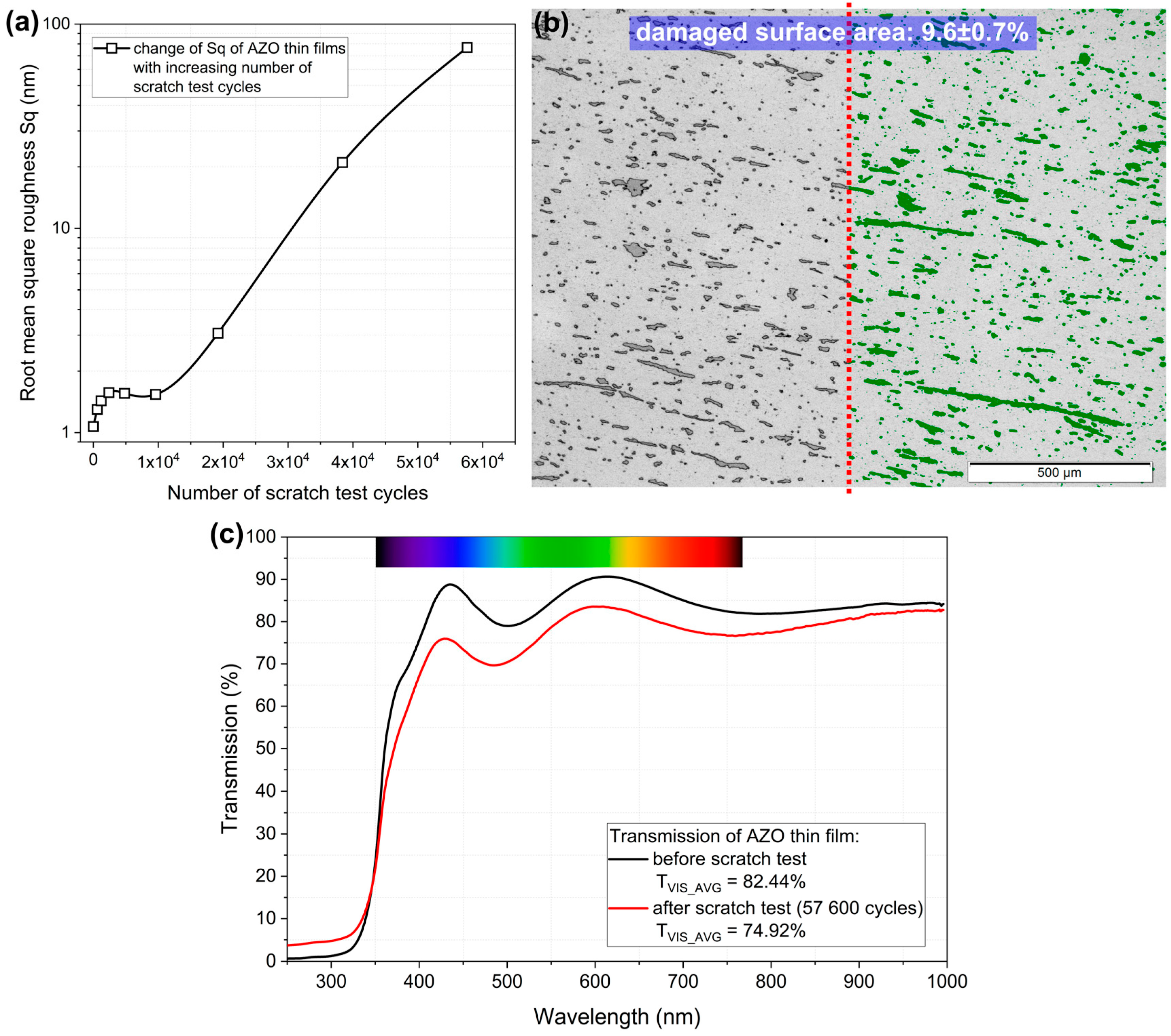
| Optical | Average transmittance in VIS (%) | 82.4 ± 0.5 | |
| Band gap energy, indirect transitions (eV) | 3.12 ± 0.05 | ||
| Cut-off wavelength (nm) | 334 ± 2 | ||
| Urbach energy (eV) | 0.17 ± 0.05 | ||
| Electrical | Sheet resistance (Ω/□) | 68 ± 2 | |
| Resistivity (Ω·cm) | 2.6 ± 0.1 × 10⁻³ | ||
| Figure of merit | 63.0 | ||
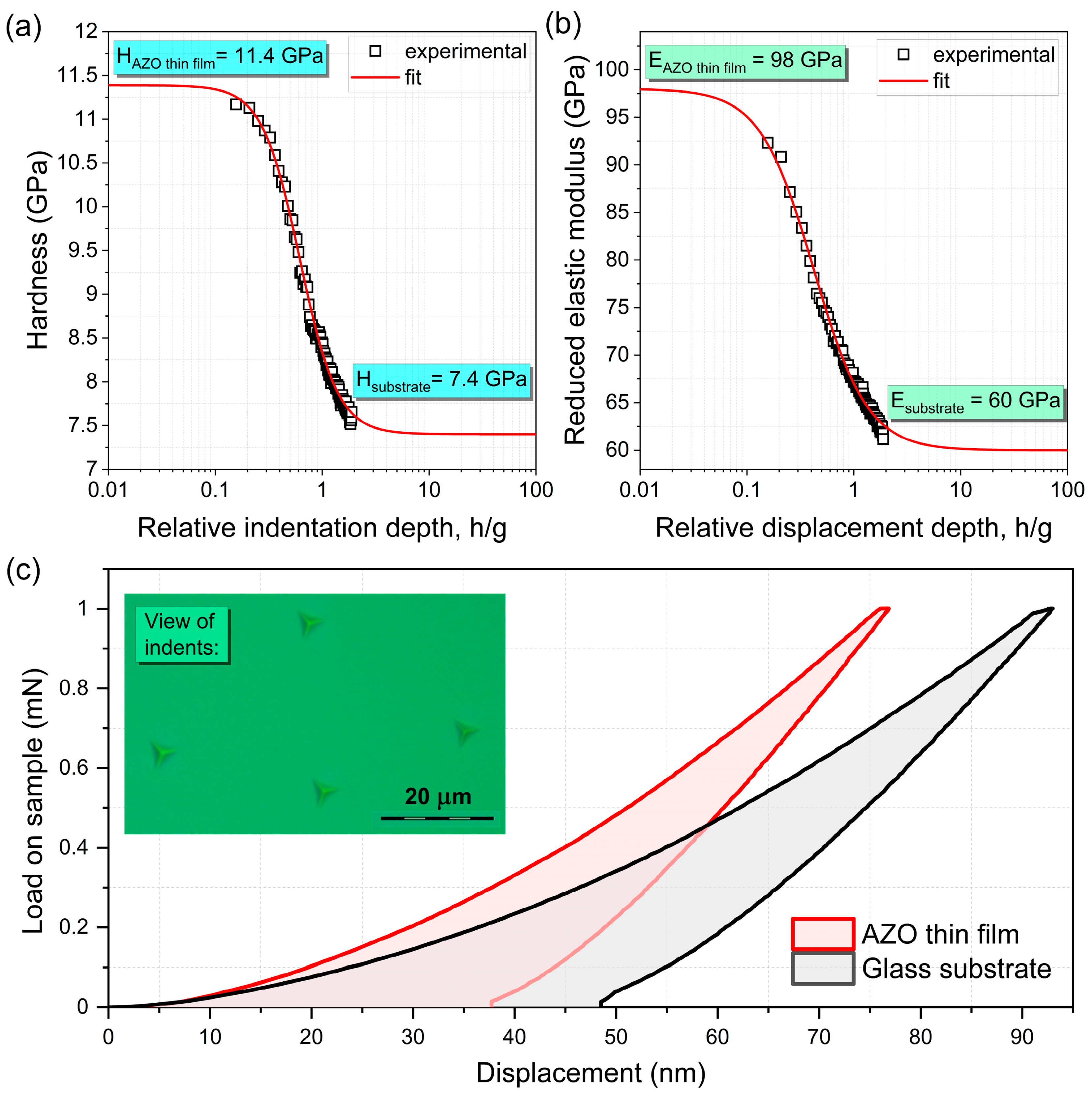
| Mechanical | Hardness (GPa) | 11.4 ± 0.4 | |
| Young’s elastic modulus (GPa) | 98.0 ± 4.1 | ||
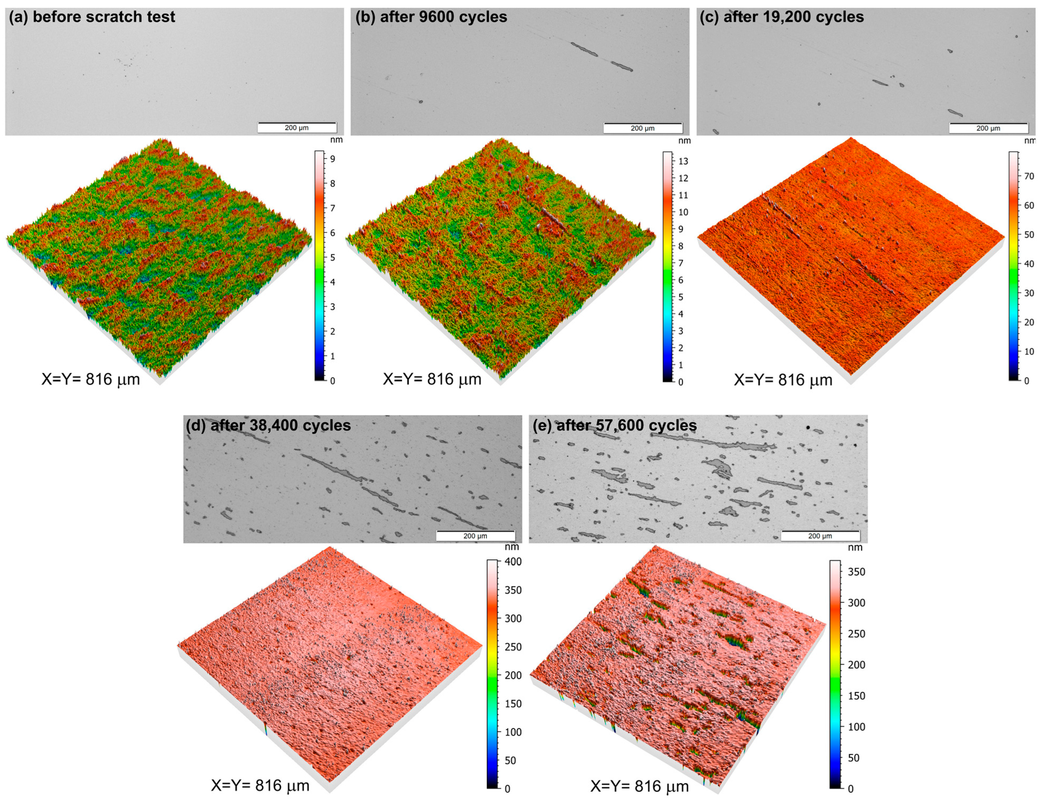
| Abrasion resistance | Sq before scratch test (nm) | 1.1 ± 0.1 | |
| Sq after scratch test (nm) | 76.8 ± 3.9 | ||
| Resistivity after scratch test (Ω∙cm) | 4.7 × 10⁻³ | ||
| Average transmittance in VIS after scratch test (%) | 74.92 ± 0.5 | ||
| Figure of merit after scratch test | 11.9 | ||
Disclaimer/Publisher’s Note: The statements, opinions and data contained in all publications are solely those of the individual author(s) and contributor(s) and not of MDPI and/or the editor(s). MDPI and/or the editor(s) disclaim responsibility for any injury to people or property resulting from any ideas, methods, instructions or products referred to in the content. |
© 2023 by the authors. Licensee MDPI, Basel, Switzerland. This article is an open access article distributed under the terms and conditions of the Creative Commons Attribution (CC BY) license (https://creativecommons.org/licenses/by/4.0/).
Share and Cite
Mazur, M.; Kiliszkiewicz, M.; Posadowski, W.; Domaradzki, J.; Małachowska, A.; Sokołowski, P. A Comprehensive Investigation of the Mechanical and Tribological Properties of AZO Transparent Conducting Oxide Thin Films Deposited by Medium Frequency Magnetron Sputtering. Materials 2024, 17, 81. https://doi.org/10.3390/ma17010081
Mazur M, Kiliszkiewicz M, Posadowski W, Domaradzki J, Małachowska A, Sokołowski P. A Comprehensive Investigation of the Mechanical and Tribological Properties of AZO Transparent Conducting Oxide Thin Films Deposited by Medium Frequency Magnetron Sputtering. Materials. 2024; 17(1):81. https://doi.org/10.3390/ma17010081
Chicago/Turabian StyleMazur, Michał, Milena Kiliszkiewicz, Witold Posadowski, Jarosław Domaradzki, Aleksandra Małachowska, and Paweł Sokołowski. 2024. "A Comprehensive Investigation of the Mechanical and Tribological Properties of AZO Transparent Conducting Oxide Thin Films Deposited by Medium Frequency Magnetron Sputtering" Materials 17, no. 1: 81. https://doi.org/10.3390/ma17010081