
Simulation of Mechanical Stresses in BaTiO3 Multilayer Ceramic Capacitors during Desoldering in the Rework of Electronic Assemblies Using a Framework of Computational Fluid Dynamics and Thermomechanical Models

Abstract
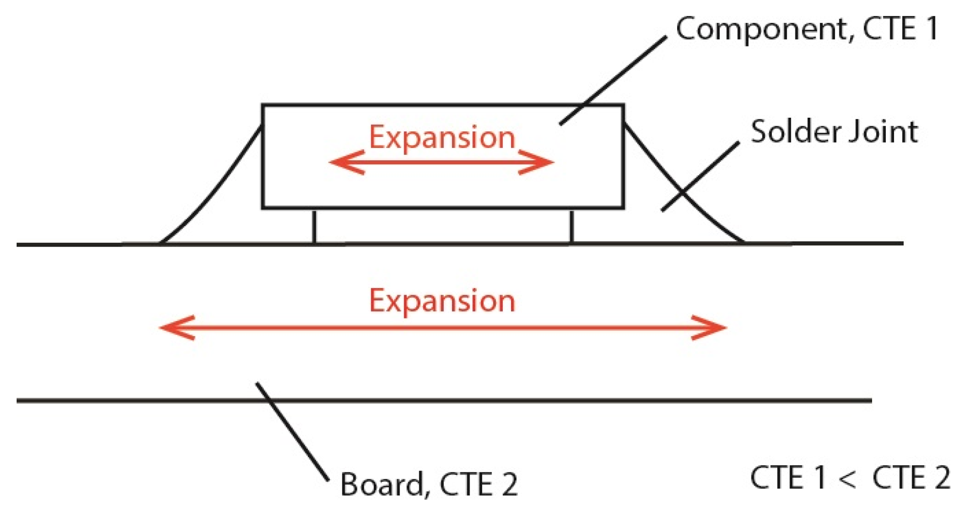
:1. Introduction
2. Materials and Methods
2.1. Experimental
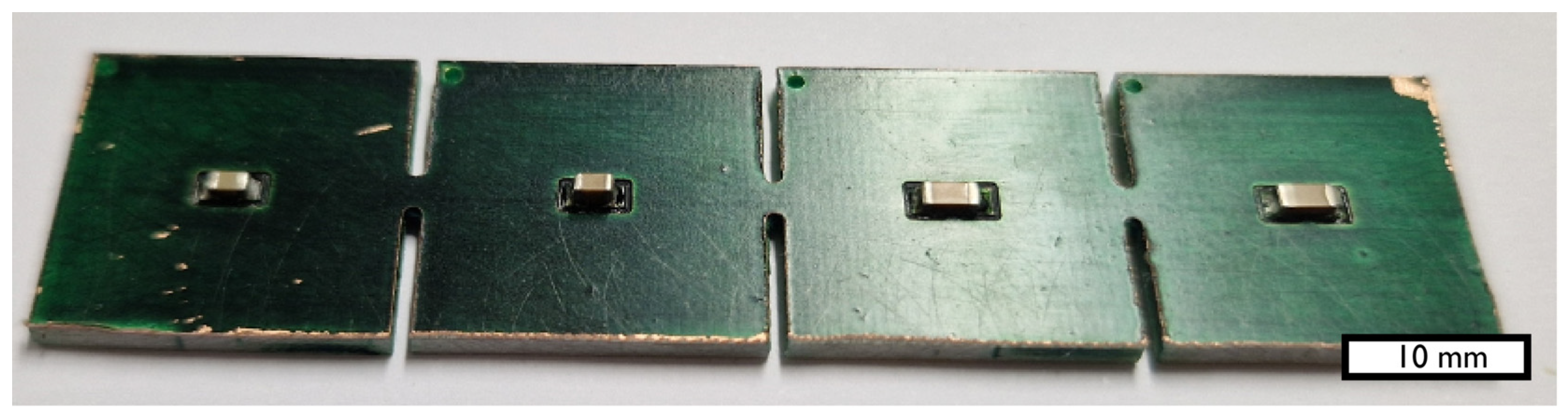
2.1.1. Board and Components
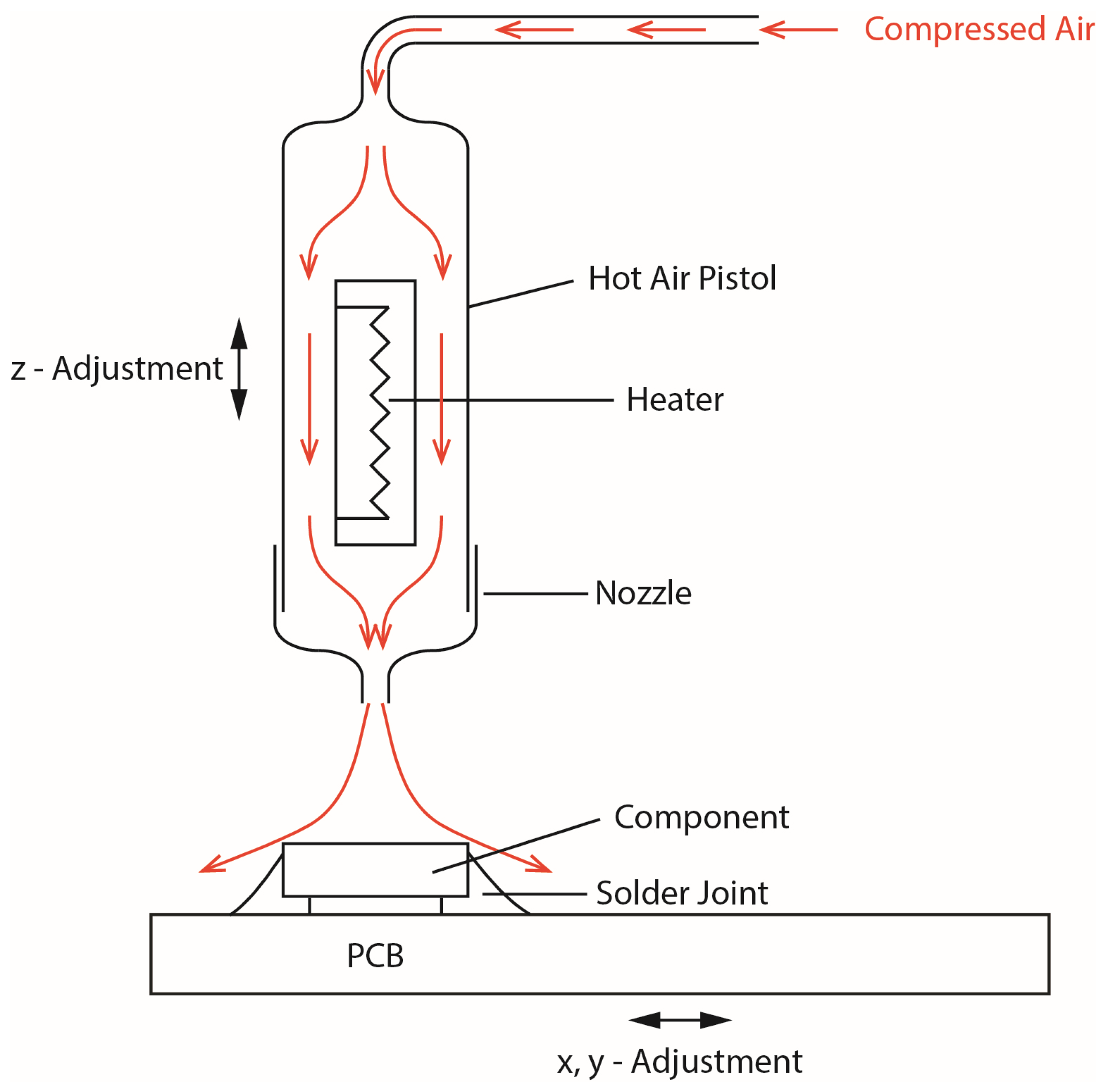
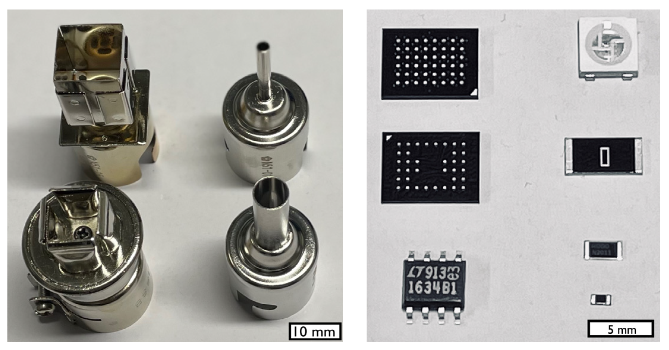
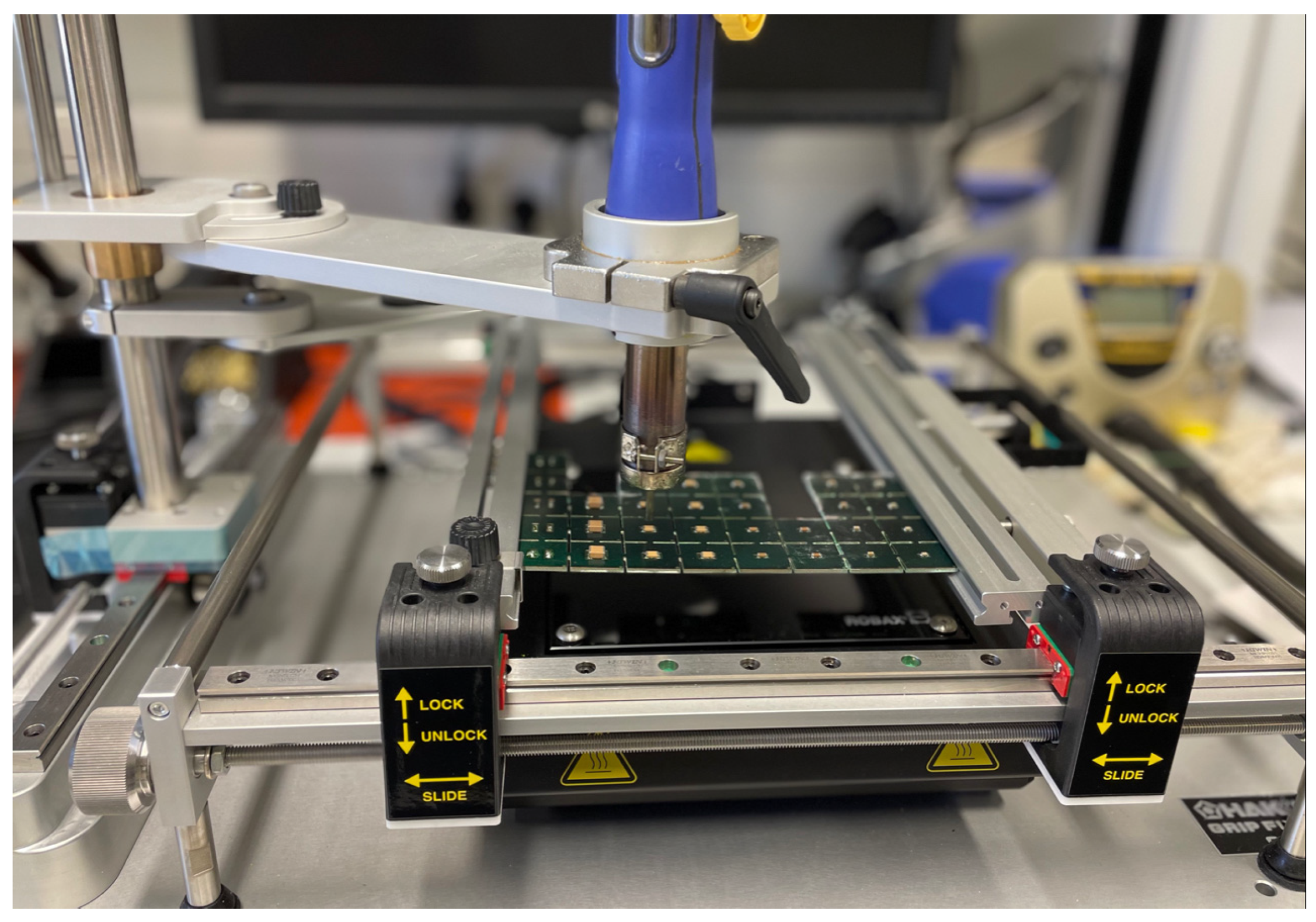
2.1.2. Rework Stations
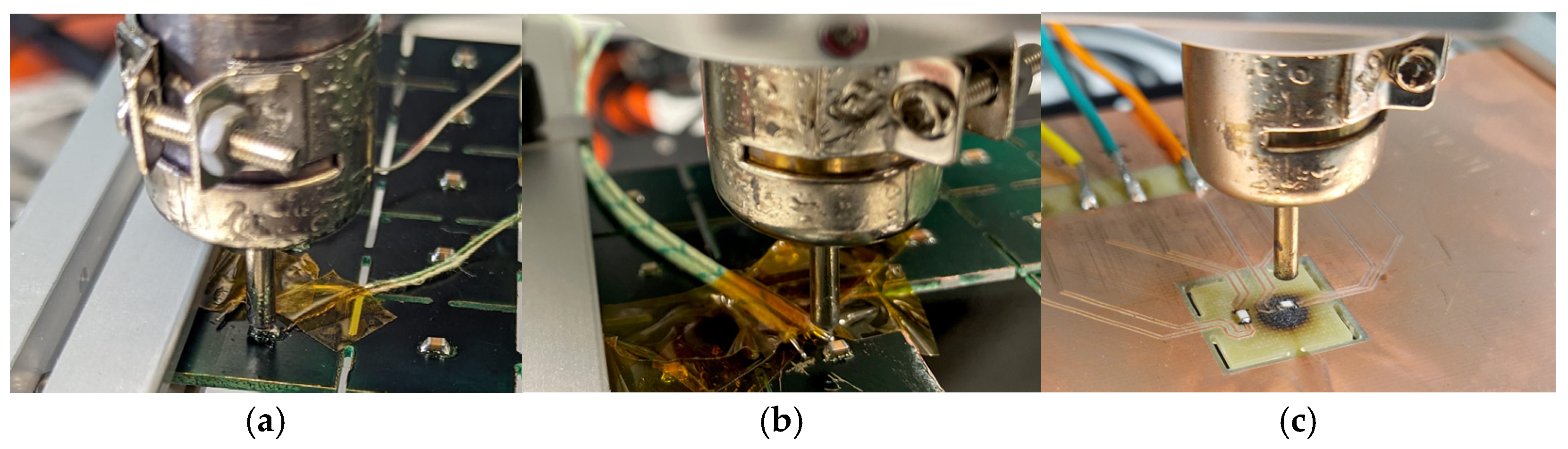
2.1.3. Temperature Measurement
2.2. Modeling
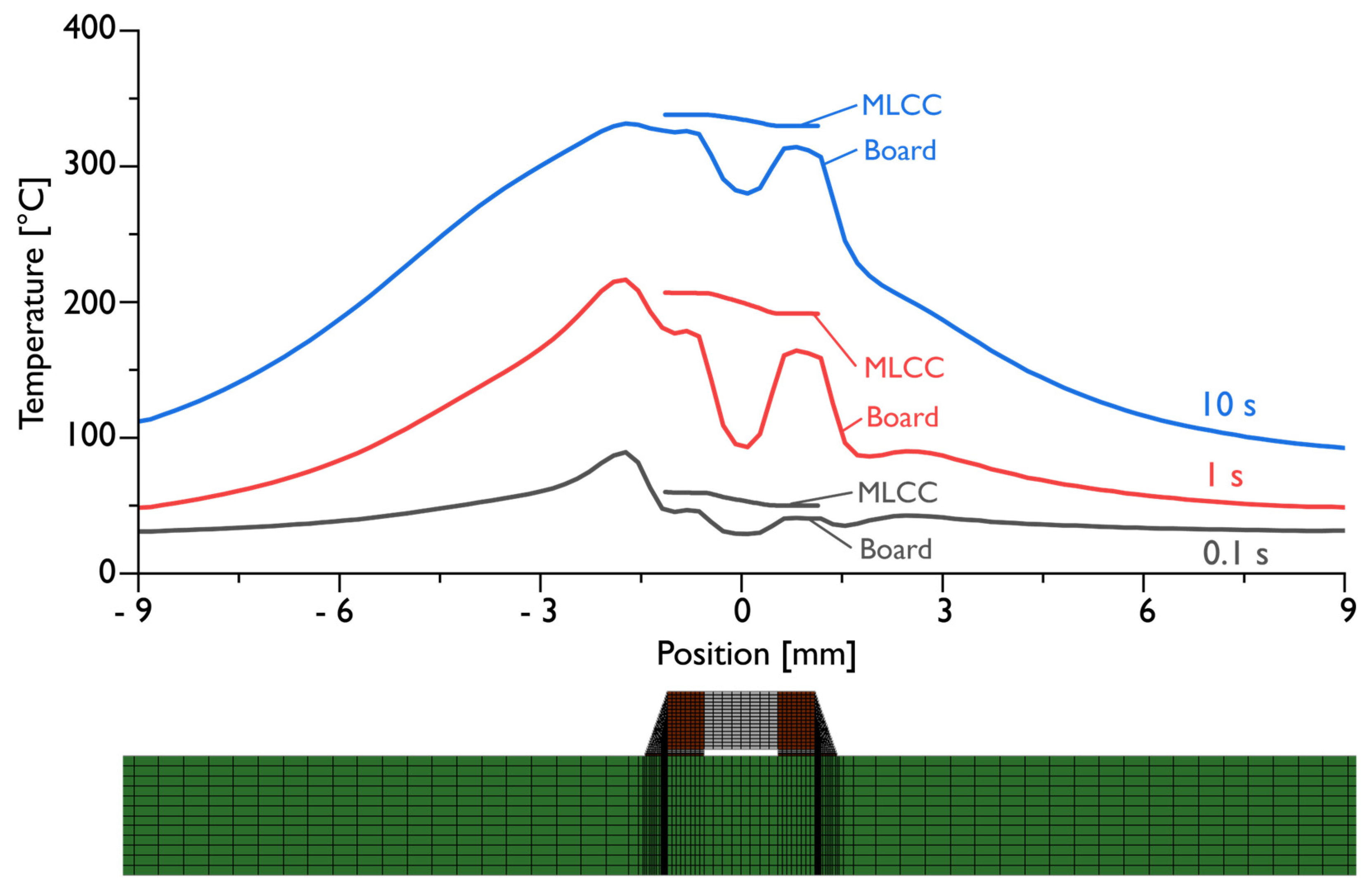
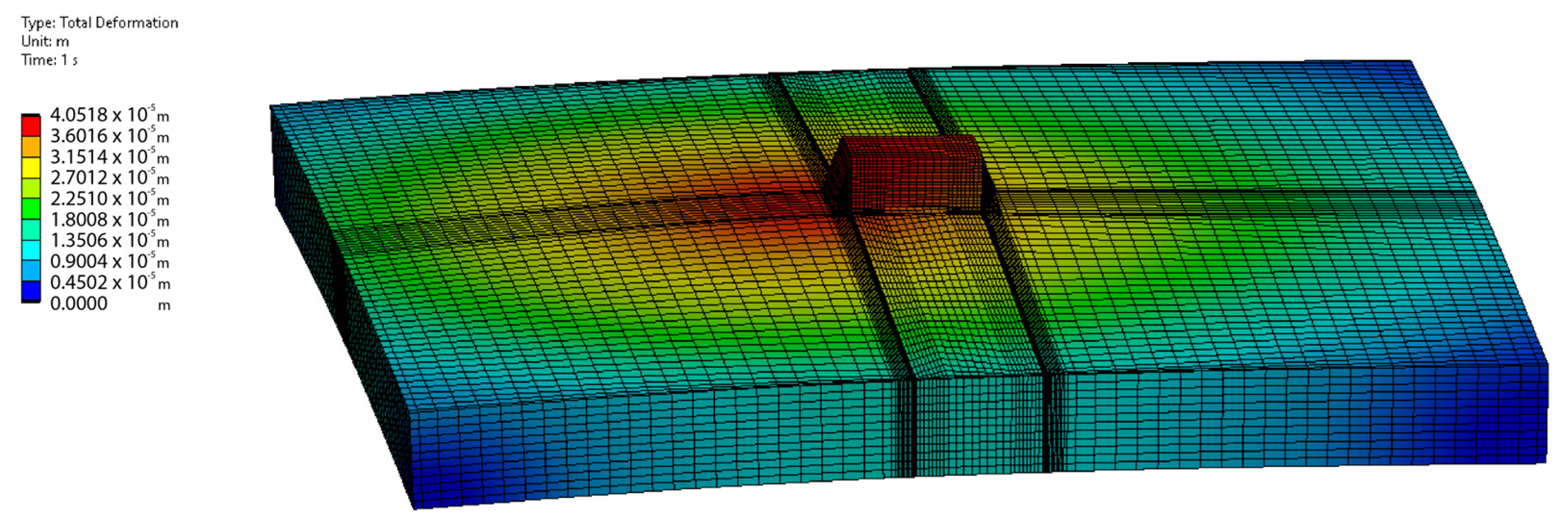
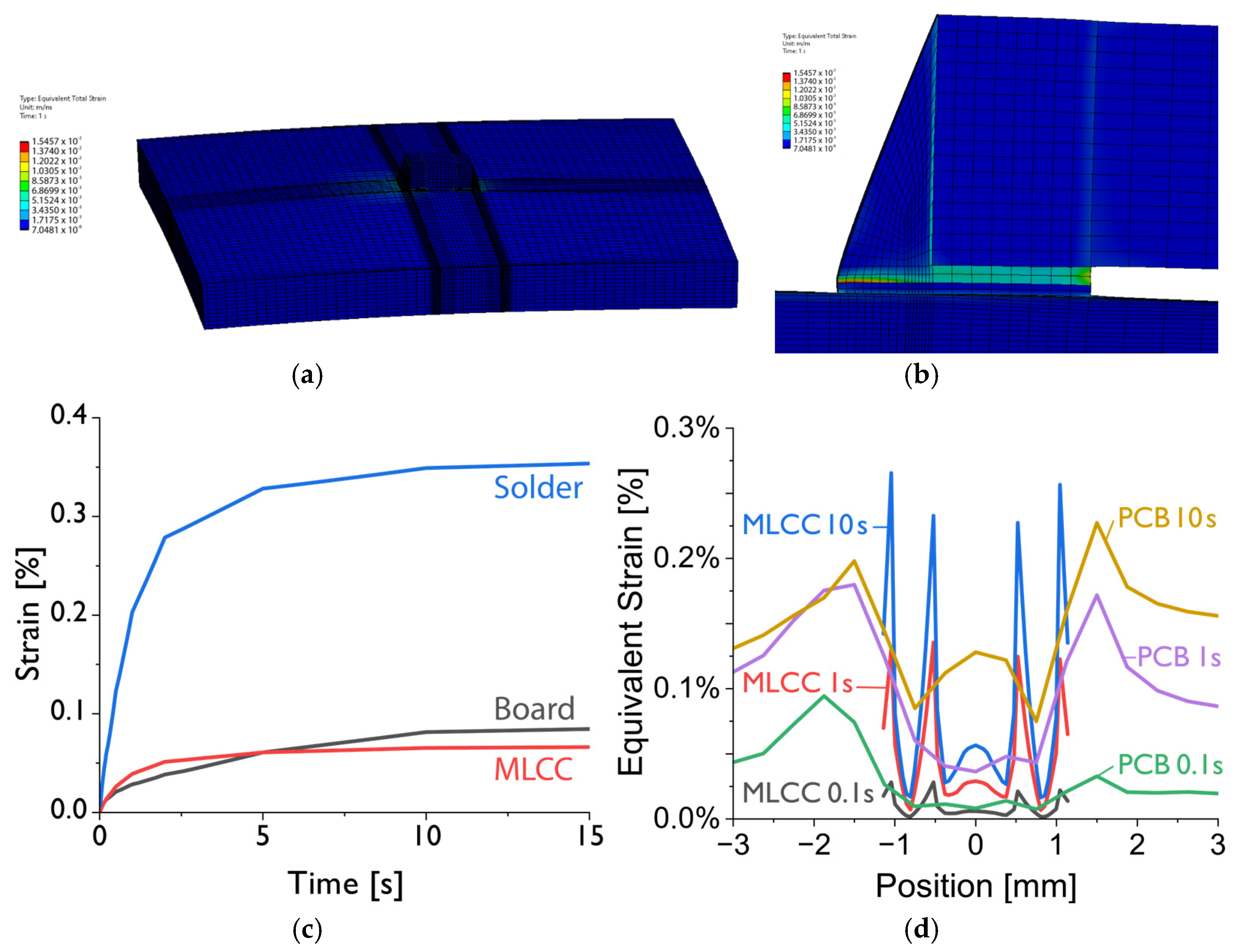
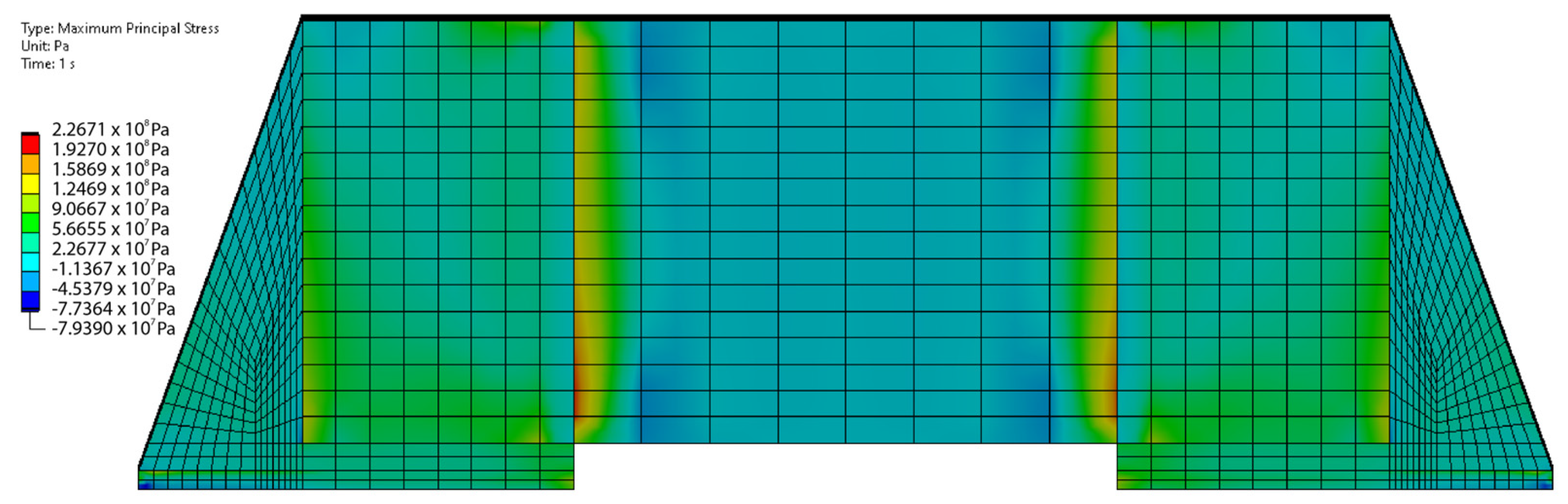
3. Results
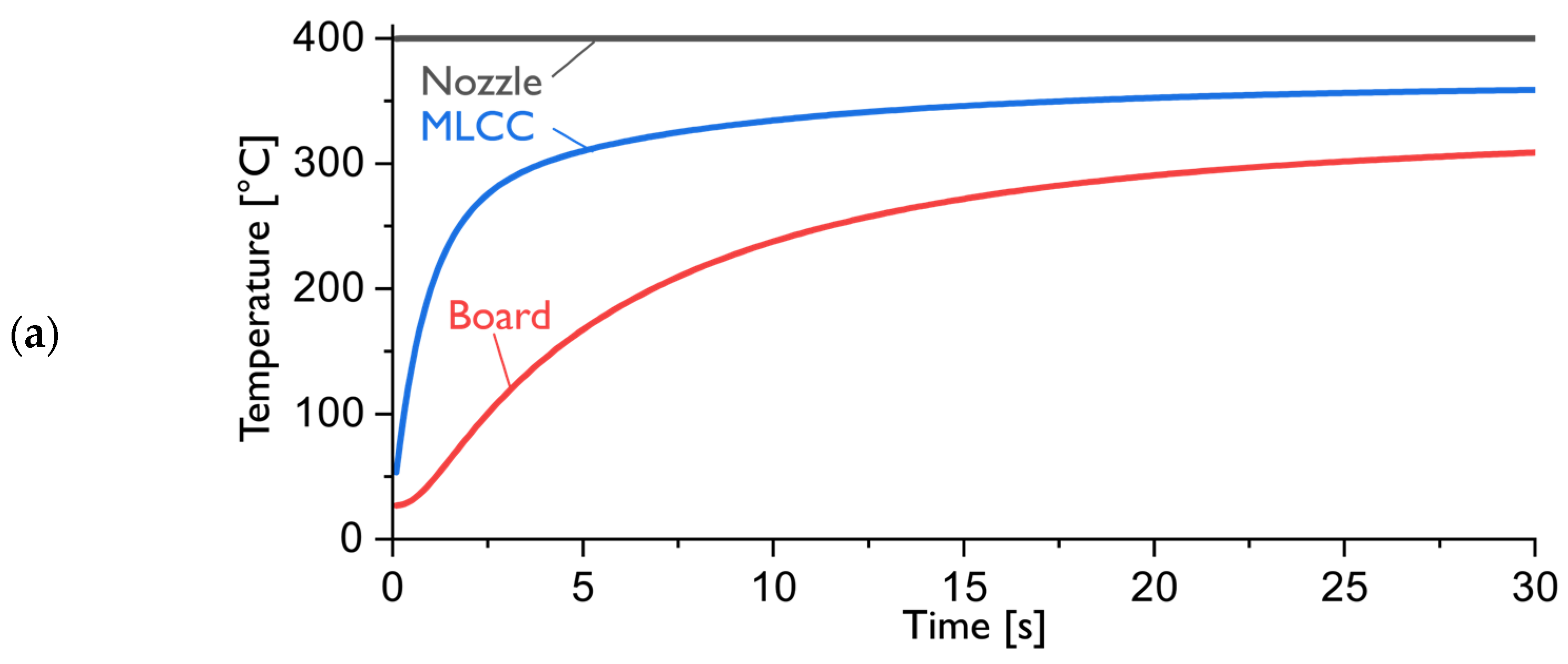
3.1. Temperature Monitoring
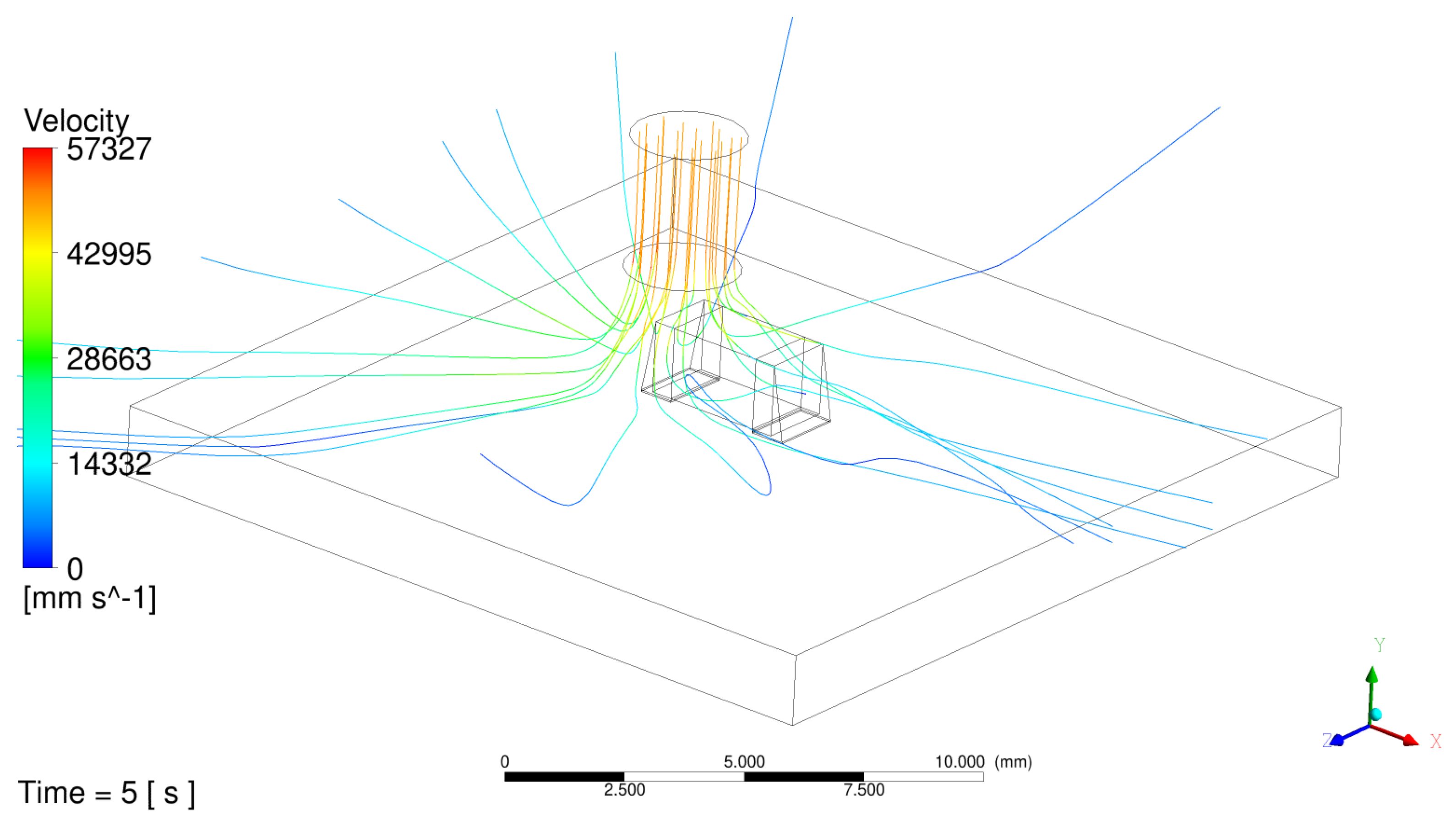
3.2. Simulation
4. Discussion
5. Conclusions
Author Contributions
Funding
Institutional Review Board Statement
Informed Consent Statement
Data Availability Statement
Conflicts of Interest
References
- Rymaszewski, E.J.; Tummala, R.R.; Watari, T. Microelectronic Packaging—An Overview. In Microelectronics Packaging Handbook—Semiconductor Packaging, Part II, 2nd ed.; Tummala, R.R., Rymaszewski, E.J., Klopfenstein, A.G., Eds.; Van Nostrand Reinhold: New York, NY, USA, 1997; pp. 3–128. [Google Scholar]
- Viswanadam, P.; Singh, P. Failure Modes and Mechanisms in Electronic Packages; Chapman & Hall: New York, NY, USA, 1998. [Google Scholar]
- Chung, D.D.L. Overview of Materials for Electronic Packaging. In Materials for Electronic Packaging; Chung, D.D.L., Ed.; Butterworth-Heinemann: Newton, MA, USA, 1995; pp. 3–39. [Google Scholar]
- Tummala, R.R. Introduction of Microsystems Packaging. In Fundamentals of Microsystems Packaging; Tummala, R.R., Ed.; McGraw-Hill: New York, NY, USA, 2001; pp. 2–42. [Google Scholar]
- Eakin, W.; Gardiner, K.; Nayak, J. Cost and performance criteria for selection of materials and processes in microelectronics packaging. J. Electron. Manuf. 1991, 1, 13–22. [Google Scholar] [CrossRef]
- Tewksbury, S.K.; Hornak, L.A. Wafer level system integration: A review. IEEE Circuits Devices Mag. 1989, 5, 22–30. [Google Scholar] [CrossRef]
- Steward, M. AVX MLCC FlexiTermTM: Guarding against Capacitor Crack Failures; AVX Technical Paper; KYOCERA AVX Components Corporation: Coleraine, UK, 2018; Available online: https://www.kyocera-avx.com/docs/techinfo/CeramicCapacitors/mlccflex.pdf (accessed on 2 June 2024).
- Ling, H.C.; Jackson, A.M. Correlation of silver migration with temperature-humidity-bias (THB) failures in multilayer ceramic capacitors. IEEE Trans. Compon. Hybrids Manuf. Technol. 1989, 12, 130–137. [Google Scholar] [CrossRef]
- Herzberger, J.L.; Dasgupta, A.; Das, S. Multiphysics study of electrochemical migration in ceramic capacitors. In Proceedings of the 16th International Conference on Thermal, Mechanical and Multi-Physics Simulation and Experiments in Microelectronics and Microsystems, Budapest, Hungary, 20–22 April 2015. [Google Scholar]
- Kim, J.; Yoon, D.; Jeon, M.; Kang, D.; Kim, J.; Lee, H. Degradation behaviors and failure analysis of Ni–BaTiO3 base-metal electrode multilayer ceramic capacitors under highly accelerated life test. Curr. Appl. Phys. 2010, 10, 1297–1301. [Google Scholar] [CrossRef]
- Yoo, Y.R.; Won, S.; Kim, Y.S. Effect of Conformal Coating on Electrochemical Migration Behavior of Multi-Layer Ceramic Capacitor for Automotives Based on Water Drop Test. Coatings 2024, 14, 359. [Google Scholar] [CrossRef]
- Sarvar, F.; Conway, P.P. Effective modeling of the reflow soldering process: Basis, construction, and operation of a process model. IEEE Trans. Compon. Packag. Manuf. Technol.-Part C 1998, 21, 126–133. [Google Scholar] [CrossRef]
- Whalley, D.C. A simplified reflow soldering process model. J. Mater. Process. Technol. 2004, 150, 134–144. [Google Scholar] [CrossRef]
- Illés, B.; Harsányi, G. Investigating direction characteristics of the heat transfer coefficient in forced convection reflow oven. Exp. Therm. Fluid Sci. 2009, 33, 642–650. [Google Scholar] [CrossRef]
- Yu, H.; Kivilathti, J. CFD modelling of the flow field inside a reflow oven. Solder. Surf. Mt. Technol. 2002, 14, 38–44. [Google Scholar] [CrossRef]
- Lau, C.S.; Abdullah, M.Z.; Ani, F.C. Computational fluid dynamic and thermal analysis for BGA assembly during forced convection reflow soldering process. Solder. Surf. Mt. Technol. 2012, 24, 77–91. [Google Scholar] [CrossRef]
- Yuile, A.; Wiese, S. Calculation of local solder temperature profiles in reflow ovens. In Proceedings of the 7th Electronic System-Integration Technology Conference (ESTC), Dresden, Germany, 18–21 September 2018. [Google Scholar]
- Dušek, K.; Rudajevová, A.; Plaček, M. Influence of latent heat released from solder joints on the reflow temperature profile. J. Mater. Sci. Mater. Electron. 2016, 27, 543–549. [Google Scholar] [CrossRef]
- Dušek, K.; Stancu, C.; Notingher, P.V.; Mach, P. Temperature distribution in solder joints during melting and solidification. In Proceedings of the 9th International Symposium on Advanced Topics in Electrical Engineering (ATEE), Bucharest, Romania, 7–9 May 2015; pp. 500–506. [Google Scholar]
- Wiese, S.; Mueller, M.; Čáp, D.; Barth, D.; Yuile, A.; Schindler, S.; Panchenko, I. Temperature evaluation of solder joints for adjusting reflow profiles. In Proceedings of the 22nd European Microelectronics and Packaging Conference & Exhibition (EMPC), Pisa, Italy, 16–19 September 2019. [Google Scholar]
- Lai, Y.; Park, S. Reflow profiling with the aid of machine learning models. Solder. Surf. Mt. Technol. 2023, 35, 257–264. [Google Scholar] [CrossRef]
- Yuile, A.; Schulz, A.; Wiss, E.; Müller, J.; Wiese, S. The Simulated Effect of Adding Solder Layers on Reactive Multilayer Films used for Joining Processes. Appl. Sci. 2022, 12, 2397. [Google Scholar] [CrossRef]
- Yuile, A.; Wiese, S. CFD analysis of wave soldering interpin behaviour. In Proceedings of the 2016 17th International Conference on Thermal, Mechanical and Multi-Physics Simulation and Experiments in Microelectronics and Microsystems (EuroSimE), Montpellier, France, 17–20 April 2016. [Google Scholar]
- Yuile, A.; Wiese, S. Simulation of temperature profiles in reflow ovens for soldering area array components. In Proceedings of the 2019 22nd European Microelectronics and Packaging Conference & Exhibition (EMPC), Pisa, Italy, 16–19 September 2019. [Google Scholar]
- Anthati, S.G.; Serea, V.; Wiss, E.; Wiese, S. FE-Analysis of Deformation State during a Four-Point Bending Experiment on Soldered MLCCs. In Proceedings of the 24th International Conference on Thermal, Mechanical and Multi-Physics Simulation and Experiments in Microelectronics and Microsystems (EuroSimE), Graz, Austria, 16–19 April 2023. [Google Scholar]
- Wiese, S.; Rzepka, S. Time-independent elastic-plastic behaviour of solder materials. Microelectron. Reliab. 2004, 44, 1893–1900. [Google Scholar] [CrossRef]


| MLCC | Size | Dimension (L × W × T) (mm) | Dielectric |
|---|---|---|---|
| KEMET C0805C684K5RACTU | 0805 | 2 × 1.25 × 1.25 | X7R |
| KEMET C1206C474K5RACTU | 1206 | 3.2 × 1.6 × 0.9 | X7R |
| KYOCERA AVX 08055G104ZAT2A | 0805 | 2.01 × 1.25 × 1.02 | Y5V |
| KYOCERA AVX 12065G105ZAT2A | 1206 | 3.20 × 1.60 × 1.27 | Y5V |
| Material | Thermal Properties | ||
|---|---|---|---|
| Density (kg/m3) | K (W/m·K) | Cp (J/kg·K) | |
| MLCC | 3474.8 | 13.739 | 772.09 |
| Terminals | 8942.5 | 396.58 | 383.48 |
| PCB | 1944.5 | 0.4899 | 962.56 |
| Solder | 7429.7 | 58.2 | 223.64 |
| Pads | 8942.5 | 396.58 | 383.48 |
| CTE (ppm/K) | Young’s Modulus (GPa) | Poisson’s Ratio | Tensile Ultimate Strength (GPa) | Tensile Yield Strength (MPa) | Bilinear Tangent Modulus (MPa) | |
|---|---|---|---|---|---|---|
| MLCC | 9.04 | 246 | 0.2392 | 20.0 | - | - |
| Terminals | 16.7 | 126 | 0.345 | 34.3 | - | - |
| PCB | 14.7 | 24.4 | 0.1649 | 29.8 | - | - |
| Solder | 24.0 | 29.9 | 0.3899 | - | 38 | 353 |
| Pads | 16.7 | 126 | 0.345 | 25.1 | - | - |
Disclaimer/Publisher’s Note: The statements, opinions and data contained in all publications are solely those of the individual author(s) and contributor(s) and not of MDPI and/or the editor(s). MDPI and/or the editor(s) disclaim responsibility for any injury to people or property resulting from any ideas, methods, instructions or products referred to in the content. |
© 2024 by the authors. Licensee MDPI, Basel, Switzerland. This article is an open access article distributed under the terms and conditions of the Creative Commons Attribution (CC BY) license (https://creativecommons.org/licenses/by/4.0/).
Share and Cite
Yuile, A.; Wiss, E.; Barth, D.; Wiese, S. Simulation of Mechanical Stresses in BaTiO3 Multilayer Ceramic Capacitors during Desoldering in the Rework of Electronic Assemblies Using a Framework of Computational Fluid Dynamics and Thermomechanical Models. Materials 2024, 17, 2702. https://doi.org/10.3390/ma17112702
Yuile A, Wiss E, Barth D, Wiese S. Simulation of Mechanical Stresses in BaTiO3 Multilayer Ceramic Capacitors during Desoldering in the Rework of Electronic Assemblies Using a Framework of Computational Fluid Dynamics and Thermomechanical Models. Materials. 2024; 17(11):2702. https://doi.org/10.3390/ma17112702
Chicago/Turabian StyleYuile, Adam, Erik Wiss, David Barth, and Steffen Wiese. 2024. "Simulation of Mechanical Stresses in BaTiO3 Multilayer Ceramic Capacitors during Desoldering in the Rework of Electronic Assemblies Using a Framework of Computational Fluid Dynamics and Thermomechanical Models" Materials 17, no. 11: 2702. https://doi.org/10.3390/ma17112702