

Piezoelectric Charge Coefficient of Halide Perovskites

Abstract
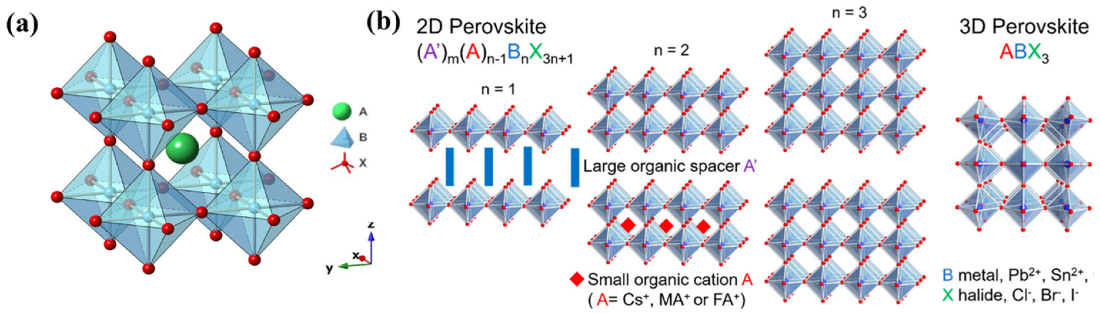
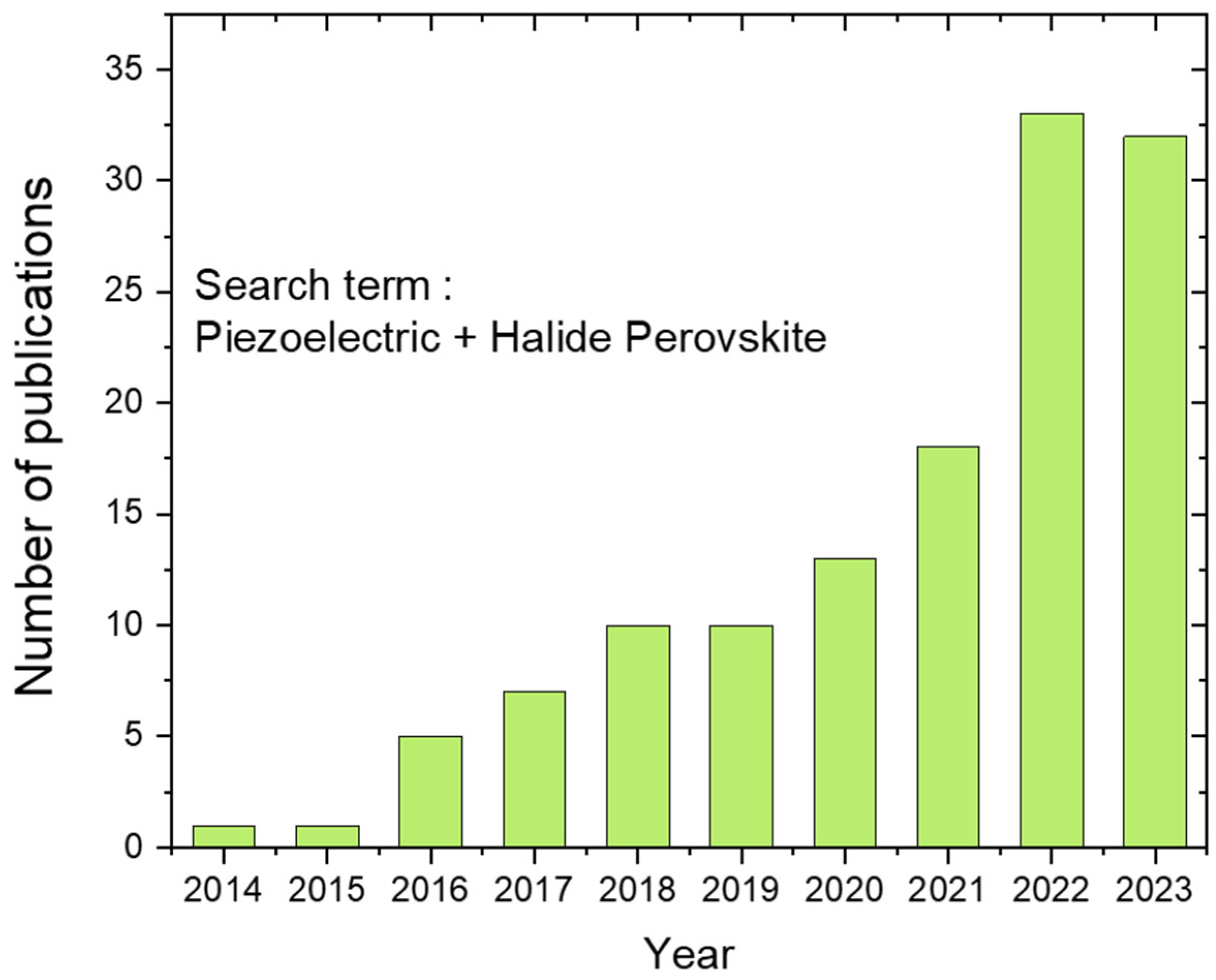
1. Introduction
2. Piezoelectric Charge Coefficient (d33)
3. Measurement Methods of Piezoelectric Charge Coefficient (d33)
- Quasi-static (Berlincourt method);
- Dynamic resonance;
- Laser interferometry;
- Piezoforce microscopy (PFM).
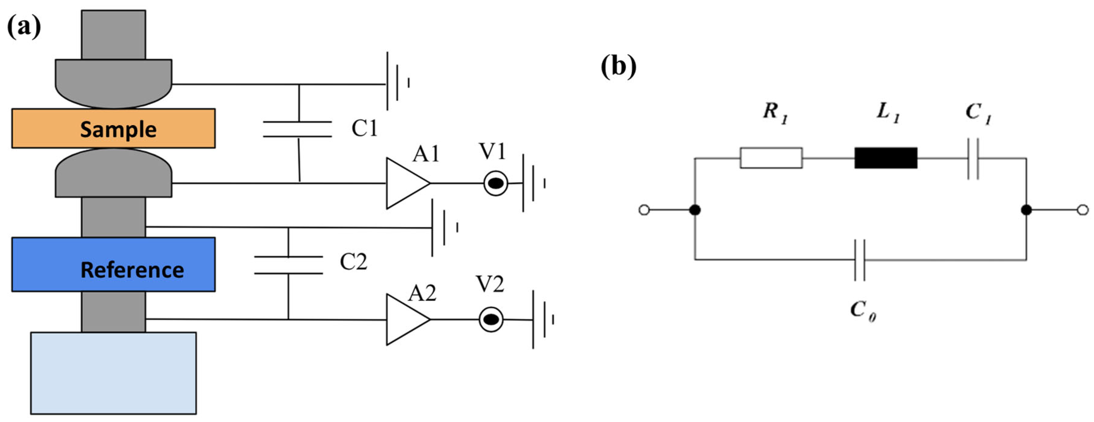
3.1. Quasi-Static Measurement Method for d33 Coefficient
3.2. Dynamic Resonance Method
3.3. Laser Interferometry Method
3.4. Piezoforce Microscopy (PFM)
4. d33 Coefficients of Halide Perovskites
4.1. d33 Coefficients of Halide Perovskite Crystals

| Halide Perovskite Composition | dij Coefficient (d33 Unless Mentioned) | Measurement Method | Curie Temperature Tc(°C) | Reference |
|---|---|---|---|---|
| MAPbI3 | 7 pC/N | Quasi-static | 58 | Ref [35] |
| MAPbI3 | 10.81 pm/N | PFM | Ref [36] | |
| FAxMA1–xPbI3 (x = 0–0.1) | 10 pC/N | Quasi-static | Ref [38] | |
| MAPbBr3 | 20 pC/N | Quasi-static | Ref [39] | |
| TMCM2SnCl6 | 137 pC/N | Quasi-static | 92 | Ref [40] |
| (ATHP)2PbBr4 | 76 pC/N | PFM | 230 | Ref [41] |
| (TMFM)x(TMCM)1–xCdCl3 (0 ≤ x ≤ 1) | 1540 pC/N | Quasi-static | 100 | Ref [42] |
| TMCMC-CdCl3, | 440 pC/N | Quasi-static | 100 | Ref [45] |
| [R- and S-1-(4-Chlorophenyl)ethylammonium]2PbI4 | 3 pm/V | PFM | Ref [46] | |
| (R-α-PEA)4Bi2I10 and (S-α-(PEA)4Bi2I10 | 32 pC/N (d22) | Quasi-static | 197 | Ref [48] |
| [(CH3)3S]3[Bi2Br9] | 18 pC/N | Quasi-static | 25 | Ref [49] |
| (BTMA)2CoBr4 | d22 5.14 pC/N d25 12.4 pC/N | Quasi-static | Ref [50] | |
| CsPb2Br5 | 72 pm/V | PFM | Ref [51] | |
| MDABCO-NH4I3 | 12.8 pm/V | PFM | 90 | Ref [52] |
4.2. d33 Coefficients of Halide Perovskite Thin Films
4.3. Dimensional Tuning of Halide Perovskites and the d33 Coefficient
5. Other Piezoelectric Factors of Halide Perovskites
Author Contributions
Funding
Data Availability Statement
Acknowledgments
Conflicts of Interest
References
- Georgiadis, A.; Collado, A.; Tentzeris, M.M. Energy Harvesting: Technologies, Systems, and Challenges; Cambridge University Press: Cambridge, UK, 2021; ISBN 9781107039377. [Google Scholar]
- Shaikh, F.K.; Zeadally, S. Energy Harvesting in Wireless Sensor Networks and Internet of Things; IET Digital library: London, UK, 2021. [Google Scholar] [CrossRef]
- Mishu, M.K.; Rokonuzzaman, M.; Pasupuleti, J.; Shakeri, M.; Rahman, K.S.; Hamid, F.A.; Tiong, S.K.; Amin, N. Prospective Efficient Ambient Energy Harvesting Sources for IoT-Equipped Sensor Applications. Electronics 2020, 9, 1345. [Google Scholar] [CrossRef]
- Malaji, P.V.; Ali, S.F.; Litak, G. Energy harvesting: Materials, structures and methods. Eur. Phys. J. Spec. Top. 2022, 231, 1355–1358. [Google Scholar] [CrossRef]
- IEA Net Zero by 2050. A Roadmap for the Global Energy Sector. Available online: https://iea.blob.core.windows.net/assets/7ebafc81-74ed-412b-9c60-5cc32c8396e4/NetZeroby2050-ARoadmapfortheGlobalEnergySector-SummaryforPolicyMakers_CORR.pdf (accessed on 10 March 2024).
- Toprak, A.; Tigli, O. Piezoelectric energy harvesting: State-of-the-art and challenges. Appl. Phys. Rev. 2014, 1, 031104. [Google Scholar] [CrossRef]
- Chalasani, S.; Conrad, J.M. A survey of energy harvesting sources for embedded systems. In Proceedings of the IEEE SoutheastCon 2008, Huntsville, AL, USA, 3–6 April 2008; pp. 442–447. [Google Scholar]
- ARM Predicts 1 Trillion IoT Devices by 2035 with New End-to-End Platform. Available online: https://www.itu.int/hub/2020/04/arm-predicts-1-trillion-iot-devices-by-2035-with-new-end-to-end-platform/ (accessed on 20 April 2024).
- Pecunia, V.; Occhipinti, L.G.; Hoye, R.L.Z. Emerging Indoor Photovoltaic Technologies for Sustainable Internet of Things. Adv. Energy Mater. 2021, 11, 2100698. [Google Scholar] [CrossRef]
- Pandey, R.; Vats, G.; Yun, J.; Bowen, C.R.; Ho-Baillie, A.W.Y.; Seidel, J.; Butler, K.T.; Seok, S. Il Mutual Insight on Ferroelectrics and Hybrid Halide Perovskites: A Platform for Future Multifunctional Energy Conversion. Adv. Mater. 2019, 31, 1807376. [Google Scholar] [CrossRef] [PubMed]
- Chatterjee, A.; Lobato, C.N.; Zhang, H.; Bergne, A.; Esposito, V.; Yun, S.; Insinga, A.R.; Christensen, D.V.; Imbaquingo, C.; Bjørk, R.; et al. Powering internet-of-things from ambient energy: A review. J. Phys Energy 2023, 5, 022001. [Google Scholar] [CrossRef]
- Liu, X.; Wei, X.; Guo, L.; Liu, Y.; Song, Q.; Jamalipour, A. Turning the Signal Interference into Benefits: Towards Indoor Self-Powered Visible Light Communication for IoT Devices in Industrial Radio-Hostile Environments. IEEE Access 2019, 7, 24978–24989. [Google Scholar] [CrossRef]
- Photovoltaic Technologies Efficiency Charge from 1976 to 2024. Available online: https://www.nrel.gov/pv/cell-efficiency.html (accessed on 20 January 2024).
- Manzi, M.; Pica, G.; De Bastiani, M.; Kundu, S.; Grancini, G.; Saidaminov, M.I. Ferroelectricity in Hybrid Perovskites. J. Phys. Chem. Lett. 2023, 14, 3535–3552. [Google Scholar] [CrossRef] [PubMed]
- Jella, V.; Ippili, S.; Eom, J.H.; Pammi, S.V.N.; Jung, J.S.; Tran, V.D.; Nguyen, V.H.; Kirakosyan, A.; Yun, S.; Kim, D.; et al. A comprehensive review of flexible piezoelectric generators based on organic-inorganic metal halide perovskites. Nano Energy 2019, 57, 74–93. [Google Scholar] [CrossRef]
- Park, H.; Ha, C.; Lee, J.H. Advances in piezoelectric halide perovskites for energy harvesting applications. J. Mater. Chem. A 2020, 8, 24353–24367. [Google Scholar] [CrossRef]
- Stranks, S.D.; Snaith, H.J. Metal-halide perovskites for photovoltaic and light-emitting devices. Nat. Nanotechnol. 2015, 10, 391–402. [Google Scholar] [CrossRef]
- Park, N.G. Perovskite solar cells: An emerging photovoltaic technology. Mater. Today 2015, 18, 65–72. [Google Scholar] [CrossRef]
- Giorgi, G.; Fujisawa, J.I.; Segawa, H.; Yamashita, K. Organic-Inorganic hybrid lead iodide perovskite featuring zero dipole moment guanidinium cations: A theoretical analysis. J. Phys. Chem. C 2015, 119, 4694–4701. [Google Scholar] [CrossRef]
- Jagadamma, L.K.; Wang, S. Wide-Bandgap Halide Perovskites for Indoor Photovoltaics. Front. Chem. 2021, 9, 71. [Google Scholar] [CrossRef]
- Mao, L.; Stoumpos, C.C.; Kanatzidis, M.G. Two-Dimensional Hybrid Halide Perovskites: Principles and Promises. J. Am. Chem. Soc. 2019, 141, 1171–1190. [Google Scholar] [CrossRef] [PubMed]
- Li, L.; Liu, X.; Li, Y.; Xu, Z.; Wu, Z.; Han, S.; Tao, K.; Hong, M.; Luo, J.; Sun, Z. Two-Dimensional Hybrid Perovskite-Type Ferroelectric for Highly Polarization-Sensitive Shortwave Photodetection. J. Am. Chem. Soc. 2019, 141, 2623–2629. [Google Scholar] [CrossRef]
- Rahmany, S.; Shpatz Dayan, A.; Wierzbowska, M.; Ong, A.J.; Li, Y.; Magdassi, S.; Tok, A.I.Y.; Etgar, L. The Impact of Piezoelectricity in Low Dimensional Metal Halide Perovskite. ACS Energy Lett. 2024, 1527–1536. [Google Scholar] [CrossRef]
- Deutz, D.B.; Pascoe, J.-A.; Schelen, B.; van der Zwaag, S.; de Leeuw, D.M.; Groen, P. Analysis and experimental validation of the figure of merit for piezoelectric energy harvesters. Mater. Horiz. 2018, 5, 444–453. [Google Scholar] [CrossRef]
- Jaffe, B.; Cook, W.R.; Jaffe, H. Chapter 3—Measurement Techniques; Academic Press: Cambridge, MA, USA, 1971; pp. 23–47. ISBN 978-0-12-379550-2. [Google Scholar]
- Li, J. Lead-Free Piezoelectric Materials; Springer: Dordrecht, The Netherlands; Heidelberg, Germany; New York, NY, USA; London, UK, 2021; p. 92. [Google Scholar]
- Stewart, M.; Cain, M.G. Characterisation of Ferroelectric Bulk Materials and Thin Films; Springer: Dordrecht, The Netherlands; Heidelberg, Germany; New York, NY, USA; London, UK, 2014; Volume 2, p. 41. [Google Scholar]
- Arnau, A.; Soares, D. Fundamentals of Piezoelectricity; Springer: Berlin/Heidelberg, Germany, 2008; pp. 1–38. [Google Scholar]
- He, L.; Feng, X.; Triantafillos, K.; Feng, N.; Bo, Z.; Ping, Y. Comparison between methods for the measurement of the D 33 constant of piezoelectric materials. In Proceedings of the 25th International Congress on Sound and Vibration, Hiroshima, Japan, 8–12 July 2018; Volume 1, pp. 77–84. [Google Scholar]
- Li, X.; Guo, M.; Dong, S. A flex-compressive-mode piezoelectric transducer for mechanical vibration/strain energy harvesting. IEEE Trans. Ultrason. Ferroelectr. Freq. Control 2011, 58, 698–703. [Google Scholar]
- Available online: https://www.eeict.cz/eeict_download/archiv/sborniky/EEICT_2011_sbornik/03-Doktorske%20projekty/03-Kybernetika%20a%20automatizace/07-xfialk02.pdf (accessed on 2 February 2024).
- Fialka, J.; Skula, D. Utilization of the Laser Interferometer for the Measurement of Piezoelectric Charge Constant D31 and D33; Wiley-VCH GmbH: Weinheim/Berlin, Germany, 2011. [Google Scholar]
- Fundamentals of Piezoelectricity. In Lead-Free Piezoelectric Materials; Wiley-VCH GmbH: Weinheim/Berlin, Germany, 2021; pp. 1–18. ISBN 9783527817047.
- Seol, D.; Kim, B.; Kim, Y. Non-piezoelectric effects in piezoresponse force microscopy. Curr. Appl. Phys. 2017, 17, 661–674. [Google Scholar] [CrossRef]
- Zhao, X.; Zhang, X.; Zhao, Z.; Wang, Y.; Yin, Y.; Li, X.; Wang, J.; Yuan, G.; Liu, J. Macroscopic piezoelectricity of an MAPbI3 semiconductor and its associated multifunctional device. Nano Energy 2023, 118, 108980. [Google Scholar] [CrossRef]
- Lai, Q.; Zhu, L.; Pang, Y.; Xu, L.; Chen, J.; Ren, Z.; Luo, J.; Wang, L.; Chen, L.; Han, K.; et al. Piezo-phototronic Effect Enhanced Photodetector Based on CH3NH3PbI3 Single Crystals. ACS Nano 2018, 12, 10501–10508. [Google Scholar] [CrossRef] [PubMed]
- Ding, Y.; Zhao, X.; Zhao, Z.; Wang, Y.; Wu, T.; Yuan, G.; Liu, J.-M. Strain-Manipulated Photovoltaic and Photoelectric Effects of the MAPbBr3 Single Crystal. ACS Appl. Mater. Interfaces 2022, 14, 52134–52139. [Google Scholar] [CrossRef]
- Zhao, X.; Zhao, Z.; Chai, Y.; Ding, Y.; Li, X.; Yan, Z.; Zhang, X.; Yuan, G.; Liu, J. Macroscopic Piezoelectricity of Halide Perovskite Single Crystals and Their Highly Sensitive Self-Powered X-ray Detectors. ACS Appl. Mater. Interfaces 2023, 15, 48375–48381. [Google Scholar] [CrossRef] [PubMed]
- Ding, Y.; Zhao, X.; Zhao, Z.; Yan, Z.; Yuan, G.; Liu, J.-M. Light and Force Multifunctional Detector Based on the Interfacial Polarization of the ITO/MAPbBr3 Schottky Junction. Adv. Opt. Mater. 2024, 12, 2301733. [Google Scholar] [CrossRef]
- Huang, G.; Khan, A.A.; Rana, M.M.; Xu, C.; Xu, S.; Saritas, R.; Zhang, S.; Abdel-Rahmand, E.; Turban, P.; Ababou-Girard, S.; et al. Achieving Ultrahigh Piezoelectricity in Organic–Inorganic Vacancy-Ordered Halide Double Perovskites for Mechanical Energy Harvesting. ACS Energy Lett. 2021, 6, 16–23. [Google Scholar] [CrossRef]
- Chen, X.-G.; Song, X.-J.; Zhang, Z.-X.; Li, P.-F.; Ge, J.-Z.; Tang, Y.-Y.; Gao, J.-X.; Zhang, W.-Y.; Fu, D.-W.; You, Y.-M.; et al. Two-Dimensional Layered Perovskite Ferroelectric with Giant Piezoelectric Voltage Coefficient. J. Am. Chem. Soc. 2020, 142, 1077–1082. [Google Scholar] [CrossRef] [PubMed]
- Liao, W.-Q.; Zhao, D.; Tang, Y.-Y.; Zhang, Y.; Li, P.-F.; Shi, P.-P.; Chen, X.-G.; You, Y.-M.; Xiong, R.-G. A molecular perovskite solid solution with piezoelectricity stronger than lead zirconate titanate. Science 2019, 363, 1206–1210. [Google Scholar] [CrossRef]
- Rotan, M.; Zhuk, M.; Glaum, J. Activation of ferroelectric implant ceramics by corona discharge poling. J. Eur. Ceram. Soc. 2020, 40, 5402–5409. [Google Scholar] [CrossRef]
- Bagheri, M.H.; Khan, A.A.; Shahzadi, S.; Rana, M.M.; Hasan, M.S.; Ban, D. Advancements and challenges in molecular/hybrid perovskites for piezoelectric nanogenerator application: A comprehensive review. Nano Energy 2024, 120, 109101. [Google Scholar] [CrossRef]
- Chen, X.-G.; Tang, Y.-Y.; Lv, H.-P.; Song, X.-J.; Peng, H.; Yu, H.; Liao, W.-Q.; You, Y.-M.; Xiong, R.-G. Remarkable Enhancement of Piezoelectric Performance by Heavy Halogen Substitution in Hybrid Perovskite Ferroelectrics. J. Am. Chem. Soc. 2023, 145, 1936–1944. [Google Scholar] [CrossRef] [PubMed]
- Yang, C.-K.; Chen, W.-N.; Ding, Y.-T.; Wang, J.; Rao, Y.; Liao, W.-Q.; Tang, Y.-Y.; Li, P.-F.; Wang, Z.-X.; Xiong, R.-G. The First 2D Homochiral Lead Iodide Perovskite Ferroelectrics: [R- and S-1-(4-Chlorophenyl)ethylammonium]2PbI4. Adv. Mater. 2019, 31, 1808088. [Google Scholar] [CrossRef] [PubMed]
- An, L.-C.; Zhao, C.; Zhao, Y.; Zhang, Y.; Li, K.; Stroppa, A.; Li, W.; Bu, X.-H. Chiral 1D Hybrid Metal Halides with Piezoelectric Energy Harvesting and Sensing Properties. Small Struct. 2023, 4, 2300135. [Google Scholar] [CrossRef]
- Tao, K.; Zhang, B.; Li, Q.; Yan, Q. Centimeter-Sized Piezoelectric Single Crystal of Chiral Bismuth-Based Hybrid Halide with Superior Electrostrictive Coefficient. Small 2023, 19, 2207663. [Google Scholar] [CrossRef] [PubMed]
- Zhang, Y.-Z.; Sun, D.-S.; Gao, J.-X.; Hua, X.-N.; Chen, X.-G.; Mei, G.-Q.; Liao, W.-Q. A Semiconducting Organic–Inorganic Hybrid Perovskite-type Non-ferroelectric Piezoelectric with Excellent Piezoelectricity. Chem.—An Asian J. 2019, 14, 1028–1033. [Google Scholar] [CrossRef]
- Guo, T.-M.; Gong, Y.-J.; Li, Z.-G.; Liu, Y.-M.; Li, W.; Li, Z.-Y.; Bu, X.-H. A New Hybrid Lead-Free Metal Halide Piezoelectric for Energy Harvesting and Human Motion Sensing. Small 2022, 18, 2103829. [Google Scholar] [CrossRef] [PubMed]
- Sahoo, A.; Paul, T.; Makani, N.H.; Maiti, S.; Banerjee, R. High piezoresponse in low-dimensional inorganic halide perovskite for mechanical energy harvesting. Sustain. Energy Fuels 2022, 6, 4484–4497. [Google Scholar] [CrossRef]
- Wu, H.-S.; Wei, S.-M.; Chen, S.-W.; Pan, H.-C.; Pan, W.-P.; Huang, S.-M.; Tsai, M.-L.; Yang, P.-K. Metal-Free Perovskite Piezoelectric Nanogenerators for Human–Machine Interfaces and Self-Powered Electrical Stimulation Applications. Adv. Sci. 2022, 9, 2105974. [Google Scholar] [CrossRef] [PubMed]
- Ippili, S.; Kim, J.H.; Jella, V.; Behera, S.; Vuong, V.H.; Jung, J.S.; Cho, Y.; Ahn, J.; Kim, I.D.; Chang, Y.H.; et al. Halide double perovskite-based efficient mechanical energy harvester and storage devices for self-charging power unit. Nano Energy 2023, 107, 108148. [Google Scholar] [CrossRef]
- Celestine, L.; Zosiamliana, R.; Gurung, S.; Bhandari, S.R.; Laref, A.; Abdullaev, S.; Rai, D.P. A Halide-Based Perovskite CsGeX3 (X = Cl, Br, and I) for Optoelectronic and Piezoelectric Applications. Adv. Theory Simul. 2024, 7, 2300566. [Google Scholar] [CrossRef]
- Coll, M.; Gomez, A.; Mas-Marza, E.; Almora, O.; Garcia-Belmonte, G.; Campoy-Quiles, M.; Bisquert, J. Polarization Switching and Light-Enhanced Piezoelectricity in Lead Halide Perovskites. J. Phys. Chem. Lett. 2015, 6, 1408–1413. [Google Scholar] [CrossRef] [PubMed]
- Ippili, S.; Jella, V.; Kim, J.; Hong, S.; Yoon, S.-G. Enhanced piezoelectric output performance via control of dielectrics in Fe2+-incorporated MAPbI3 perovskite thin films: Flexible piezoelectric generators. Nano Energy 2018, 49, 247–256. [Google Scholar] [CrossRef]
- Song, J.; Xiao, Z.; Chen, B.; Prockish, S.; Chen, X.; Rajapitamahuni, A.; Zhang, L.; Huang, J.; Hong, X. Enhanced Piezoelectric Response in Hybrid Lead Halide Perovskite Thin Films via Interfacing with Ferroelectric PbZr0.2Ti0.8O3. ACS Appl. Mater. Interfaces 2018, 10, 19218–19225. [Google Scholar] [CrossRef] [PubMed]
- Kim, D.B.; Park, K.S.; Park, S.J.; Cho, Y.S. Microampere-level piezoelectric energy generation in Pb-free inorganic halide thin-film multilayers with Cu interlayers. Nano Energy 2022, 92, 106785. [Google Scholar] [CrossRef]
- Kim, D.B.; Park, K.H.; Cho, Y.S. Origin of high piezoelectricity of inorganic halide perovskite thin films and their electromechanical energy-harvesting and physiological current-sensing characteristics. Energy Environ. Sci. 2020, 13, 2077–2086. [Google Scholar] [CrossRef]
- Ippili, S.; Jella, V.; Eom, J.-H.; Kim, J.; Hong, S.; Choi, J.-S.; Tran, V.-D.; Van Hieu, N.; Kim, Y.-J.; Kim, H.-J.; et al. An eco-friendly flexible piezoelectric energy harvester that delivers high output performance is based on lead-free MASnI3 films and MASnI3-PVDF composite films. Nano Energy 2019, 57, 911–923. [Google Scholar] [CrossRef]
- Khan, A.A.; Rana, M.M.; Wang, S.; Fattah, M.F.A.; Kayaharman, M.; Zhang, K.; Benedict, S.; Goldthorpe, I.A.; Zhou, Y.N.; Sargent, E.H.; et al. Control of Halogen Atom in Inorganic Metal-Halide Perovskites Enables Large Piezoelectricity for Electromechanical Energy Generation. Small 2023, 19, 2303366. [Google Scholar] [CrossRef] [PubMed]
- Kim, D.B.; Jo, K.S.; Park, K.S.; Cho, Y.S. Anion-Dependent Polarization and Piezoelectric Power Generation in Hybrid Halide MAPbX3 (X = I, Br, and Cl) Thin Films with Out-of-Plane Structural Adjustments. Adv. Sci. 2023, 10, 2204462. [Google Scholar] [CrossRef] [PubMed]
- Sahoo, S.; Deka, N.; Boomishankar, R. Piezoelectric energy harvesting of a bismuth halide perovskite stabilised by chiral ammonium cations. CrystEngComm 2022, 24, 6172–6177. [Google Scholar] [CrossRef]
- He, L.; Liu, Y.; Shi, P.; Cai, H.; Fu, D.; Ye, Q. Energy Harvesting and Pd(II) Sorption Based on Organic–Inorganic Hybrid Perovskites. ACS Appl. Mater. Interfaces 2020, 12, 53799–53806. [Google Scholar] [CrossRef]
- Rana, M.M.; Khan, A.A.; Zhu, W.; Fattah, M.F.A.; Kokilathasan, S.; Rassel, S.; Bernard, R.; Ababou-Girard, S.; Turban, P.; Xu, S.; et al. Enhanced piezoelectricity in lead-free halide perovskite nanocomposite for self-powered wireless electronics. Nano Energy 2022, 101, 107631. [Google Scholar] [CrossRef]
- Hou, Y.; Wu, C.; Yang, D.; Ye, T.; Honavar, V.G.; van Duin, A.C.T.; Wang, K.; Priya, S. Two-dimensional hybrid organic–inorganic perovskites as emergent ferroelectric materials. J. Appl. Phys. 2020, 128, 60906. [Google Scholar] [CrossRef]
- Pandey, R.; SB, G.; Grover, S.; Singh, S.K.; Kadam, A.; Ogale, S.; Waghmare, U.V.; Rao, V.R.; Kabra, D. Microscopic Origin of Piezoelectricity in Lead-Free Halide Perovskite: Application in Nanogenerator Design. ACS Energy Lett. 2019, 4, 1004–1011. [Google Scholar] [CrossRef]
- Garcia, M.P.; Gibson, D.; Hughes, D.A.; Nuñez, C.G. A Refined Quasi-Static Method for Precise Determination of Piezoelectric Coefficient of Nanostructured Standard and Inclined Thin Films. Adv. Phys. Res. 2024, 3, 2300091. [Google Scholar] [CrossRef]
- Huang, Z.; Zhang, Q.; Corkovic, S.; Dorey, R.; Whatmore, R.W. Comparative measurements of piezoelectric coefficient of PZT films by berlincourt, interferometer, and vibrometer methods. IEEE Trans. Ultrason. Ferroelectr. Freq. Control 2006, 53, 2287–2293. [Google Scholar] [CrossRef] [PubMed]
- Guan, Z.; Jiang, Z.-Z.; Tian, B.-B.; Zhu, Y.-P.; Xiang, P.-H.; Zhong, N.; Duan, C.-G.; Chu, J.-H. Identifying intrinsic ferroelectricity of thin film with piezoresponse force microscopy. AIP Adv. 2017, 7, 95116. [Google Scholar] [CrossRef]
- Shimizu, T.; Katayama, K.; Kiguchi, T.; Akama, A.; Konno, T.J.; Sakata, O.; Funakubo, H. The demonstration of significant ferroelectricity in epitaxial Y-doped HfO2 film. Sci. Rep. 2016, 6, 32931. [Google Scholar] [CrossRef] [PubMed]
- Zhang, Y.; Roscow, J.; Xie, M.; Bowen, C. High piezoelectric sensitivity and hydrostatic figures of merit in unidirectional porous ferroelectric ceramics fabricated by freeze casting. J. Eur. Ceram. Soc. 2018, 38, 4203–4211. [Google Scholar] [CrossRef]
- Lee, M.K.; Kim, B.H.; Lee, G.J. Piezoelectric voltage constant and sensitivity enhancements through phase boundary structure control of lead-free (K,Na)NbO3-based ceramics. J. Eur. Ceram. Soc. 2022, 42, 4898–4906. [Google Scholar] [CrossRef]
- Khan, A.A.; Huang, G.; Rana, M.M.; Mei, N.; Biondi, M.; Rassel, S.; Tanguy, N.; Sun, B.; Leonenko, Z.; Yan, N.; et al. Superior transverse piezoelectricity in organic-inorganic hybrid perovskite nanorods for mechanical energy harvesting. Nano Energy 2021, 86, 106039. [Google Scholar] [CrossRef]
- Rathore, S.; Leong, W.L.; Singh, A. Mechanical properties estimation of 2D–3D mixed organic-inorganic perovskites based on methylammonium and phenylethyl-ammonium system using a combined experimental and first-principles approach. J. Alloys Compd. 2023, 936, 168328. [Google Scholar] [CrossRef]
- Govinda, S.; Kore, B.P.; Bokdam, M.; Mahale, P.; Kumar, A.; Pal, S.; Bhattacharyya, B.; Lahnsteiner, J.; Kresse, G.; Franchini, C.; et al. Behavior of Methylammonium Dipoles in MAPbX3 (X = Br and I). J. Phys. Chem. Lett. 2017, 8, 4113–4121. [Google Scholar] [CrossRef] [PubMed]
- Zhang, C.; Wei, W.; Sun, H.; Zhu, Q. Performance enhancements in poly(vinylidene fluoride)-based piezoelectric films prepared by the extrusion-casting process. J. Mater. Sci. Mater. Electron. 2021, 32, 21837–21847. [Google Scholar] [CrossRef]

| Halide Perovskite Composition | dij Coefficient (d33 Unless Mentioned) | Measurement Method | Reference | |
|---|---|---|---|---|
| MAPbI3 | 5 pm/N | PFM | 58 | Ref [55] |
| Fe: MAPbI3 | 17.5 pm/N | PFM | ~44–47 | Ref [56] |
| CsPbI3 | 15 pm/N | PFM | Ref [58] | |
| CsPbBr3 | 23 pm/N | PFM | 130 | Ref [59] |
| MAPbCl3 | 3.4 pm/N | PFM | Ref [62] | |
| MAPbBr3 | 4.9 pm/N | PFM | Ref [62] | |
| MASnI3 | 20 pm/V | PFM | 30 | Ref [60] |
| CsPbI2Br | 47 pm/V | PFM | 130 | Ref [61] |
Disclaimer/Publisher’s Note: The statements, opinions and data contained in all publications are solely those of the individual author(s) and contributor(s) and not of MDPI and/or the editor(s). MDPI and/or the editor(s) disclaim responsibility for any injury to people or property resulting from any ideas, methods, instructions or products referred to in the content. |
© 2024 by the authors. Licensee MDPI, Basel, Switzerland. This article is an open access article distributed under the terms and conditions of the Creative Commons Attribution (CC BY) license (https://creativecommons.org/licenses/by/4.0/).
Share and Cite
Sekhar Muddam, R.; Sinclair, J.; Krishnan Jagadamma, L. Piezoelectric Charge Coefficient of Halide Perovskites. Materials 2024, 17, 3083. https://doi.org/10.3390/ma17133083
Sekhar Muddam R, Sinclair J, Krishnan Jagadamma L. Piezoelectric Charge Coefficient of Halide Perovskites. Materials. 2024; 17(13):3083. https://doi.org/10.3390/ma17133083
Chicago/Turabian StyleSekhar Muddam, Raja, Joseph Sinclair, and Lethy Krishnan Jagadamma. 2024. "Piezoelectric Charge Coefficient of Halide Perovskites" Materials 17, no. 13: 3083. https://doi.org/10.3390/ma17133083
APA StyleSekhar Muddam, R., Sinclair, J., & Krishnan Jagadamma, L. (2024). Piezoelectric Charge Coefficient of Halide Perovskites. Materials, 17(13), 3083. https://doi.org/10.3390/ma17133083