Article

A Metamaterials-Based Absorber Used for Switch Applications with Dynamically Variable Bandwidth in Terahertz Regime

1
School of Microelectronics, Shenzhen Institute of Information Technology, Shenzhen 518172, China
2
Digital and Intelligent Agriculture Research Institute, School of Information Engineering, Huzhou University, Huzhou 313000, China
*
Author to whom correspondence should be addressed.
Materials 2024, 17(14), 3571; https://doi.org/10.3390/ma17143571
Submission received: 23 June 2024 / Revised: 16 July 2024 / Accepted: 16 July 2024 / Published: 19 July 2024

Abstract

:
A broadband absorber based on metamaterials of graphene and vanadium dioxide (VO2) is proposed and investigated in the terahertz (THz) regime, which can be used for switch applications with a dynamically variable bandwidth by electrically and thermally controlling the Fermi energy level of graphene and the conductivity of VO2, respectively. The proposed absorber turns ‘on’ from 1.5 to 5.4 THz, with the modulation depth reaching 97.1% and the absorptance exceeding 90% when the Fermi energy levels of graphene are set as 0.7 eV, and VO2 is in the metallic phase. On the contrary, the absorptance is close to zero and the absorber turns ‘off’ with the Fermi energy level setting at 0 eV and VO2 in the insulating phase. Furthermore, other four broadband absorption modes can be achieved utilizing the active materials graphene and VO2. The proposed terahertz absorber may benefit the areas of broadband switch, cloaking objects, THz communications and other applications.

1. Introduction

Metamaterials, which usually consists of periodically arranged artificial unit cells with a sub-wavelength structure, possess outstanding electromagnetic properties [1]. Metamaterials-based applications have been found in many researching fields, such as metalenses [2], optical cloaking [3,4], sensors [5,6], biomedical research [7], and filters [8,9]. Since the first metamaterial absorber (MA) designed by Landy et al. in 2008 [10], a variety of MAs have been widely proposed and investigated, such as the absorbers with narrowband [11,12], multi-band [13,14,15], and broadband [16,17,18]. Among this research, metamaterials-based terahertz (THz) absorbers, working from 0.1 to 10 THz, have been given extensive attention for their promising application in future wireless communication [19,20]. However, the traditional MAs generally have only a single function, and the metamaterial layers are usually composed of periodically arranged metallic patterns, which are limited in practical applications for the fixed geometrical dimensions.
The reconfigurable characteristics of MAs can be realized by utilizing active materials such as phase transition materials [21,22], liquid metals [23], liquid crystals [24], ferroelectrics [25], photoconductive silicon [26,27], and 2D materials [28]. In recent years, graphene, with its unique electrical properties [29] such as high electron mobility, flexible tunability, relatively low loss and tight field confinement, has shown promising application in multifunctional THz devices [30,31,32,33,34]. The electromagnetic properties of the graphene-based MAs can be dynamically tuned by adjusting the Fermi energy level through chemical doping or electrostatic gating [35]. Moreover, vanadium dioxide (VO2), undergoing an insulator-metal transition process at the temperature around 340 K [36], plays a very active role in the switchable devices [37,38].
Zhang et al. have designed a MA based on strontium titanate and bulk Dirac semimetal. The absorption could be modulated in two modes, including single-band and dual-band, by thermally controlling the conductivity of VO2 and electrically changing the Fermi energy level of graphene [39]. Similar MAs based on active materials [40,41,42,43,44,45] usually work in one or two fixed frequency bands once the structure is fabricated, as shown in Table 1. Moreover, most MAs with two absorption modes show narrow relative bandwidth (RB) defined by RB = bandwidth/center frequency. Although a few absorbers show a relative large RB, the absorption broadband is fixed [44].
Herein, we proposed a metamaterials-based absorber in THz regime, which could be used for switch applications with multiple dynamic broadband absorption modes and large RB. When VO2 is in the metallic phase, and the Fermi energy levels of the graphene are simultaneously set as 0.7 eV, the broadband absorption can be achieved from 1.5 to 5.4 THz with the absorptance exceeding 90%, which indicates the state ‘on’ for switch application, and the relative bandwidth can reach 113%. When the Fermi energy level of graphene is 0 eV, the absorption of the proposed absorber exhibited a state transition from ‘on’ to ‘off’ by thermally controlling the conductivity of VO2 patterns and film. The physical mechanism of the broadband absorption is investigated by analyzing the distributions of the electric field and surface currents. Furthermore, the influence of the parameters on the broadband absorption is also investigated to guide the real fabrication of the proposed absorber. In addition, the other four broadband absorption modes can be realized by electrically and thermally adjusting the active material graphene and VO2, respectively. Generally, the proposed absorber promises switch application with various bandwidths.

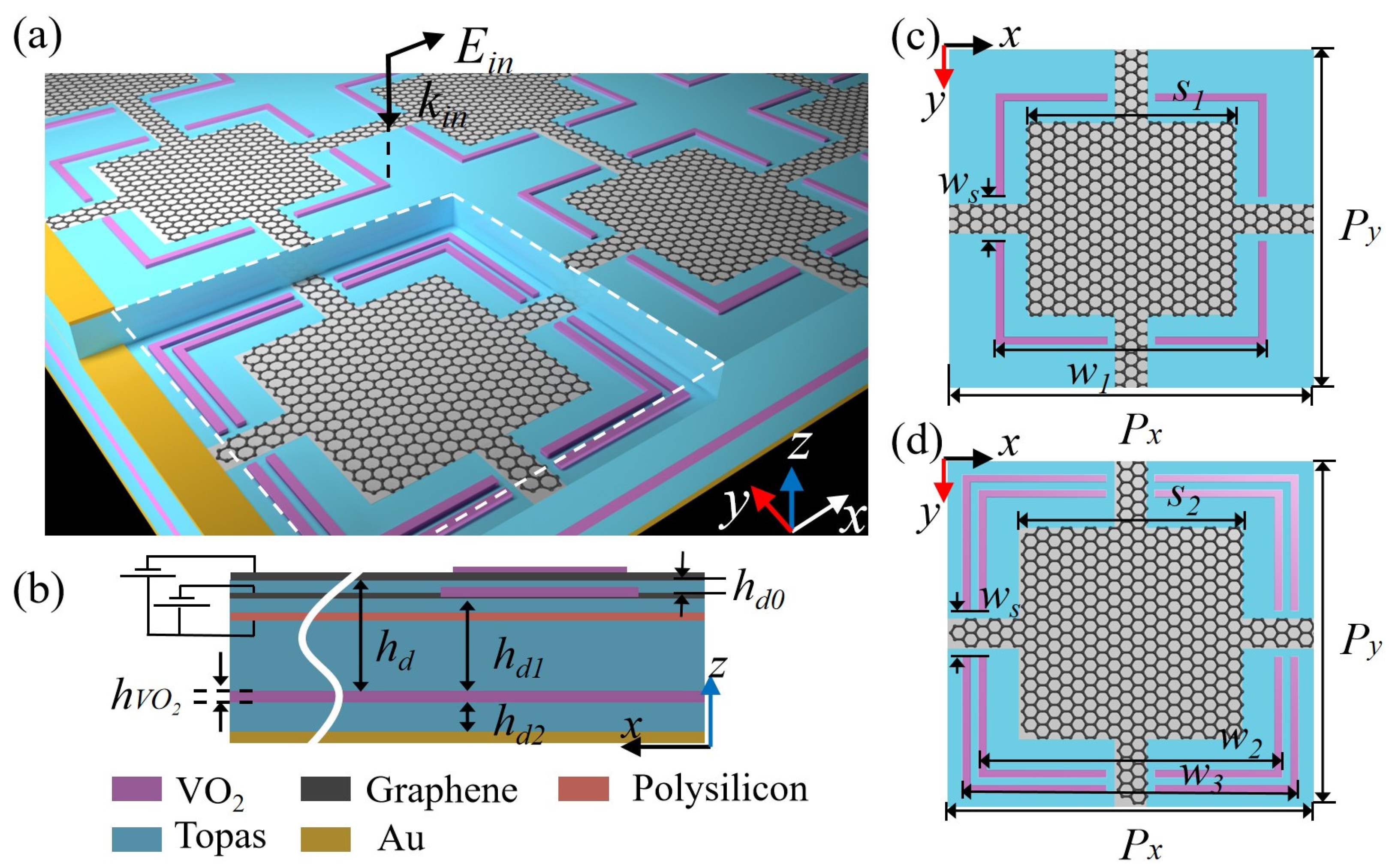
2. Materials and Methods

The proposed absorber consists of two metamaterial layers, a polysilicon sheet, a VO2 film, and a bottom gold (Au) plane, top to bottom, separating with polyethylene cyclic olefin copolymer (Topas) as depicted in Figure 1a,b. The connected graphene square and a VO2 split loop constitute the unit cell of the upper metamaterial layer, as shown in Figure 1c, and the unit cell of the lower metamaterial layer is also formed by the graphene square, apart from two VO2 split loops, as shown in Figure 1d. Both the width of the VO2 split loops as well as the spacer between the two VO2 split loops is fixed as 1 μm. The split gaps of the 200-nm-thick VO2 loops are set as ws. Topas is used as the insulating spacer for the proposed absorber, which has negligible loss and dispersion in the THz regime, and the relative permittivity of Topas is set as 2.35 [46]. The polysilicon sheet with extremely excellent semiconductor characteristics serves as the bottom electrode for controlling the Fermi energy level of graphene. The extremely thin (20 nm) polysilicon sheet has almost no influence on the absorption. The periods of the unit cell are Px on the x-direction and Py on the y-direction. The detailed dimensions of the proposed absorber are listed in Table 2.
The proposed absorber is numerically investigated by the finite element solver COMSOL Multiphysics (6.0, Stockholm, Sweden). The insulating phase and the metallic phase of VO2 are described with conductivities of 0 S/m and 2 × 10⁵ S/m, respectively. The optical characteristics of vanadium dioxide is defined by the dielectric permittivity, which is described by the Drude model [33]:
ε ( ω ) = ε ω p 2 ( σ ) ω 2 + i γ ω ,
where ε = 12 is the dielectric permittivity at the infinite frequency, γ = 5.75 × 10¹³ rad/s is the collision frequency, and ωp(σ) is the plasma frequency. When σ0 = 3 × 10⁵ S/m, the value of plasma frequency is 1.4 × 10¹⁵ rad/s.
Graphene is simulated as a 2D material in the simulation. More specifically, graphene is modeled as a surface current J = σgEt in the frequency domain according to Ohm’s law, where σg is the conductivity of graphene and Et is the tangential electric field on the graphene layer [47]. The complex surface conductivity of graphene can be described by the Kubo formula: σg(ω, τ, μc) = σintra(ω, τ, μc) + σinter(ω, τ, μc). The interband and intraband transition contributions are expressed as [48]:
σ inter ( w , τ , μ c ) j e 2 4 π ln [ 2 | μ c | ( ω + j / π ) 2 | μ c | + ( ω + j / π ) ] ,
σ intra ( w , τ , μ c ) j e 2 k B T π 2 ( ω 2 + j τ 1 ) [ μ c k B T + 2 ln ( exp ( μ c k B T ) + 1 ) ] ,
where T, ω, τ = μEfe−1υF−2, kB, μc, and ħ ≈ 1.055 × 1034 J·s are the temperature in Kelvin, incident angular frequency, relaxation time, Boltzmann constant, chemical potential, and reduced Planck constant, respectively. The chemical potential μc is equal to the Fermi energy level Ef for kB < μc. The relaxation time τ is 0.1 ps for μ = 1500 cm2V−1s−1 and Ef = 0.7 eV.
According to the formula, the conductivity of graphene is a function related to the temperature. When the temperature varies from 50 K to 400 K, corresponding to the VO2 varying from metallic phase to insulating phase, the conductivity of graphene changes little in the frequency range from 0.5 to 6.5 THz, as shown in Figure 2. It is well known that the temperature of the surrounding environment is much lower than 340 K, at which the VO2 undergoes an insulator–metal transition process. The bias voltage applied on the graphene layer has a limited impact on the temperature of surrounding environment, i.e., the optical characteristics of VO2 are insensitive to the changes in the Fermi energy level of graphene. Consequently, these two tunable methods almost do not interfere with each other. In practice, the CVD-grown graphene layer can be transferred onto the multilayer substrate by a transfer technique using polymethylmethacrylate (PMMA) supporting layers, and is subsequently patterned by photolithography and oxygen plasma etching [49]. A vanadium film can be sputtered onto the lower Topas layer at room temperature and subsequently converted into VO2 under O2 ambient at 375 °C, and then subsequently patterned by e-beam lithography [50].

3. Results and Discussion

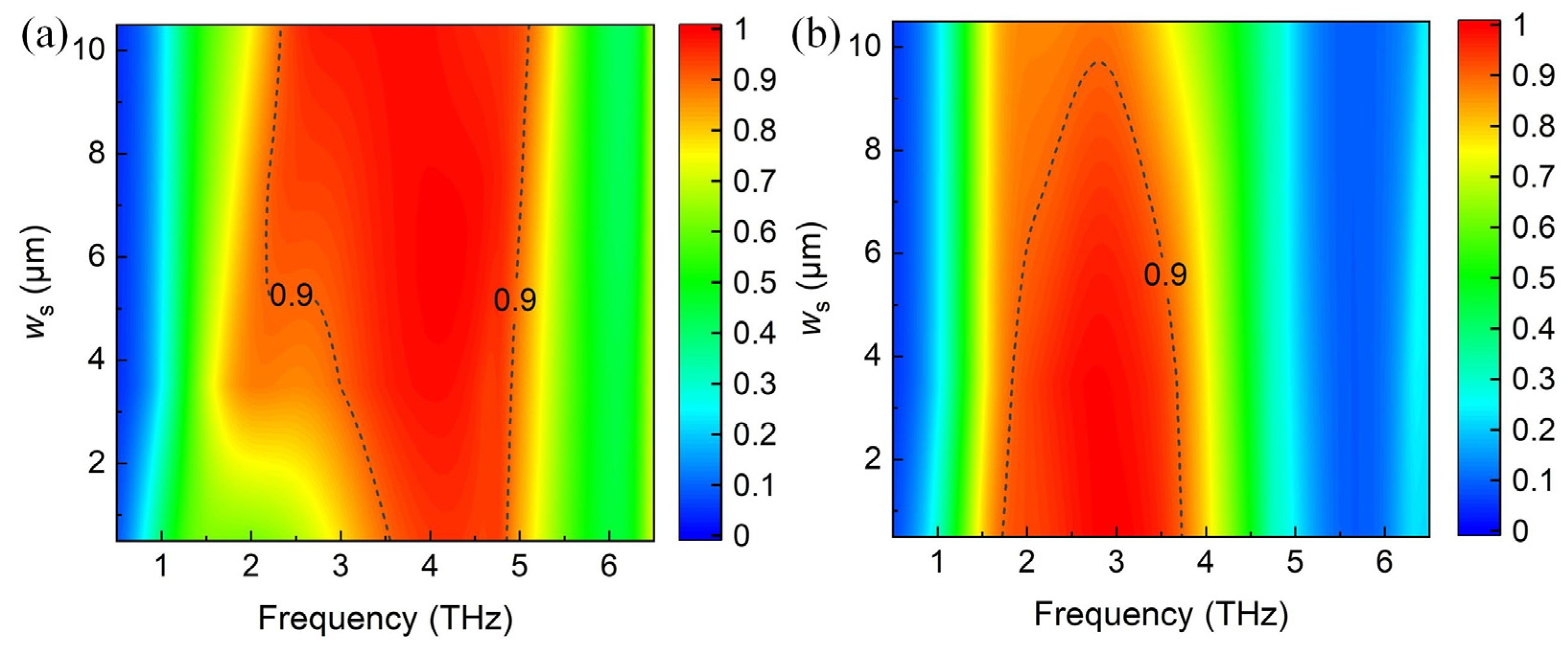
3.1. Broadband Absorber Used for Switch Applications

The intensity of absorptance A is expressed by A = 1 − TR, where transmittance T = |S21|2 and reflectance R = |S11|2. The absorption spectra of the broadband absorber is shown in Figure 3. The relative bandwidth is 113%. According to the investigation of the active materials, graphene and VO2, the switch control can be realized via external voltage and ambient temperature, respectively. When the Fermi energy level of the two graphene layers are set as 0.7 eV, and VO2 is in the metallic phase, the proposed absorber is turned ‘on’ from 1.5 to 5.4 THz with the absorptance exceeding 90%, as depicted by the dashed curve. Correspondingly, the proposed absorber turns ‘off’ when the Fermi energy level of the two graphene layers are set as 0 eV, and VO2 is in the insulating phase, as depicted by the solid curve. The employment of an electric voltage as the stimuli contributes to a fast switch, while the thermal accumulation takes some time. Thus, the response time of switching from the ‘off’ to the ’on’ state takes from picoseconds to several minutes depending on the strength and duration of excitation, as well as the initial temperature and thermal mass of the VO2 component [51,52]. Modulation depth (MD) is introduced to measure the performance for switch application, which can be expressed by MD = (AmaxAmin)/Amax. Then, a THz switch with the excellent value of MD (97.1%) is realized.
To clarify the physical mechanism of the proposed absorber, the electric field and the current distributions are investigated. Figure 4a–c show the distributions of the electric field and current at the first resonance, 1.7 THz, for the upper metamaterial layer, the lower metamaterial layer and the VO2 film, respectively. The electric field is concentrated between the top and bottom gaps of VO2 split loops, and also on the edges. The direction of surface currents on the graphene layers is parallel to the electric field of the incident wave, which indicates an electric resonance [53]. The direction of the currents (represented by the yellow long arrows) on the horizontal VO2 splits of metamaterial layers (both the upper and lower layers) are antiparallel to those of the currents on the VO2 film, which form a loop and result in a strong magnetic resonance, as shown in Figure 4a,b. In contrast, the currents on the vertical VO2 splits are negligible. The investigation can be confirmed by the distributions of the magnetic field |H| in Figure 5a. For the vertical VO2 splits in the lower metamaterial layer, the currents show an opposite direction, which can be viewed as an electric quadrupole moment [54]. In addition, for the horizontal VO2 splits in both the upper and lower metamaterial layers, the currents show the same direction, which can be viewed as an electric dipole moment.
The current distributions of the upper metamaterial layer and the VO2 film at the center frequency 3.45 THz are similar to that at 1.7 THz, as shown in Figure 4d,f. The currents on horizontal VO2 splits in lower metamaterial layers are all heading in the same direction, while the currents on the vertical splits show opposite directions. Therefore, this phenomenon results in the electric dipole moment and electric quadrupole moment. The distributions of the magnetic field |H| at 3.45 THz are shown in Figure 5b. The electric field amplitude distributions at the second resonance, 5.05 THz, show electric dipole moment and electric quadrupole moment, as indicated in Figure 4g,h. Different from the resonance frequency, 1.7 THz, Figure 4h,i show that the magnetic resonance at 5.05 THz can be attributed to the antiparallel currents between the lower graphene layer and the VO2 film, and then a strong magnetic field is obtained, as shown in Figure 5c. Therefore, profiting from the combination of magnetic resonance and electrical resonance, the incident waves are consumed, and an excellent broadband absorption can be achieved from 1.5 to 5.4 THz.
In order to further distinguish the influences of the upper and lower metamaterial layers, we investigate the absorption spectra varying with ws without the upper or lower layer, as shown in Figure 6. It is clear that the proposed absorber with a single metamaterial layer will result in a reduction in bandwidth. The upper metamaterial layer mainly affects the high frequency absorption, as shown in Figure 6a, while the lower metamaterial layer plays an important role in the low frequency absorption, as shown in Figure 6b. Combining the influence of ws on the absorption spectra in Figure 6a,b, ws is optimized as 5.5 μm in the simulation.
Subsequently, the influence of key structural parameters on the broadband absorption is investigated to guide the real fabrication of the proposed absorber, as shown in Figure 7. It can be seen from Figure 7a that when hd increases, the first and second resonances appear red-shifted with different degrees due to the influence of the magnetic resonance, and the absorption bandwidth narrows. Figure 7b shows the influence of the space hd0 between the two metamaterial layers with a fixed value of hd. It is clear that the first resonance varies slightly, while the second resonance shows significant changes. This phenomenon can be explained by the hd1 decrease as the increment of hd0 for the fixed hd. Then, the decreasing hd1 influences the magnetic resonance between the lower graphene layer and the VO2 film. In Figure 7c, the condition is set as: when w3 increases, w1 and w2 also increase, with a fixed spacer and width of VO2 loops. Thus, the two resonances show red shift due to the increasing effective length of the LC circuit model. The variety of ws has little influence on the absorption bandwidth, as shown in Figure 7d. The influence of Fermi energy level and the conductivity of VO2 on absorption spectra is investigated in Figure 7e,f, respectively. In order to optimize the parameters, 0.7 eV and 2 × 10⁵ S/m is chosen as the final value of Fermi energy level and the conductivity of VO2, respectively.

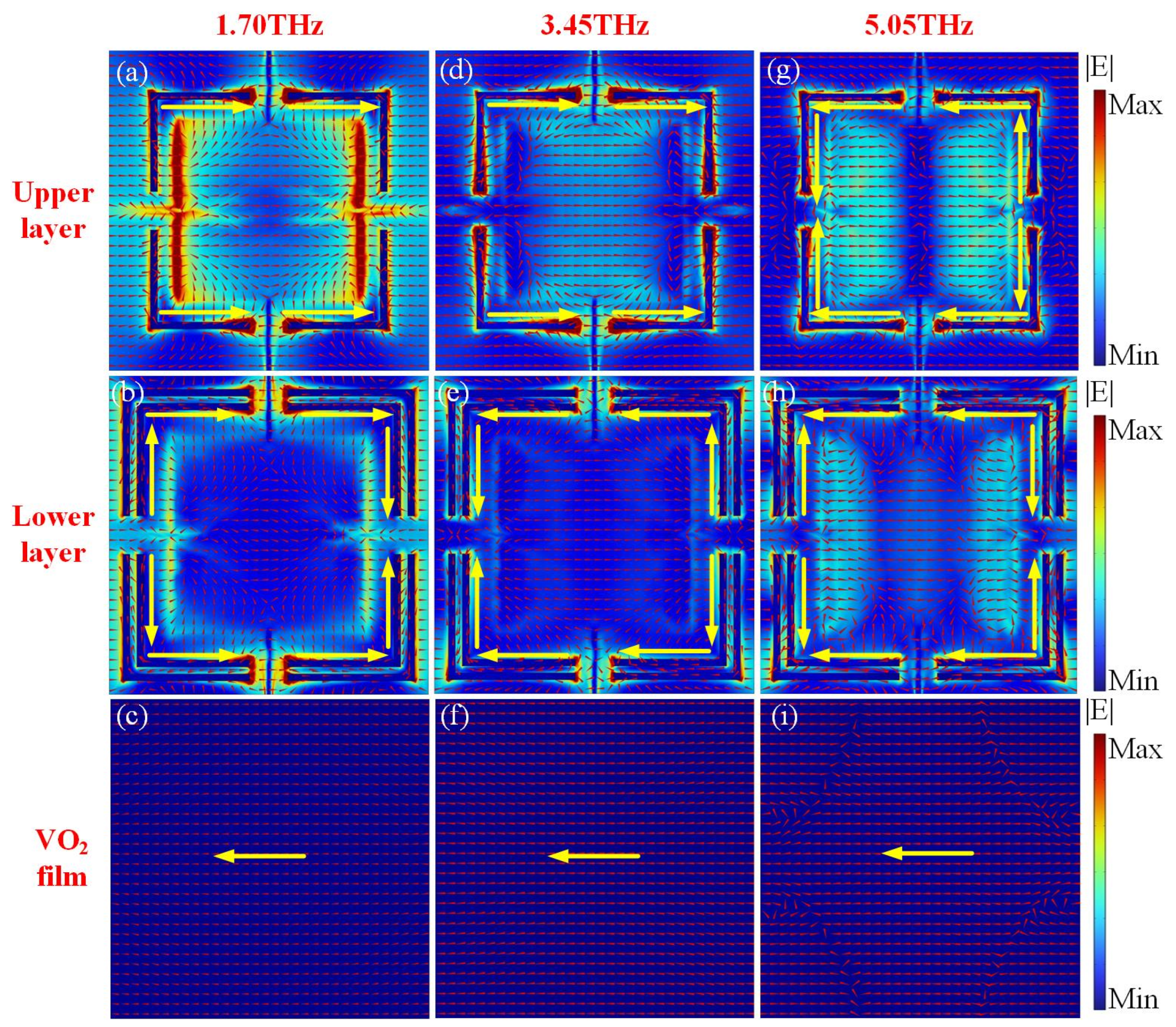
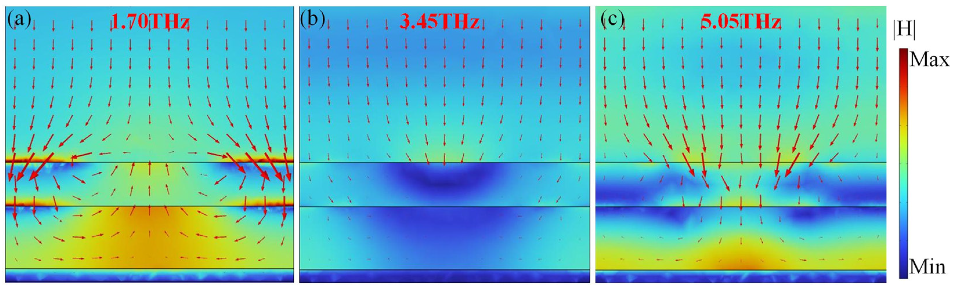
3.2. Multiple Broadband Absorption Modes

The proposed broadband absorber can further realize multiple broadband absorption modes, utilizing the active materials graphene and VO2. Figure 8 shows the absorption spectra of the proposed absorber in the insulating phase, and the Fermi energy level varies from 0.3 to 0.7 eV. The bandwidth of the absorption spectra ranges from 1.2 to 2.45 THz with Ef1 = Ef2 = 0.7 eV. The amplitude can also be adjusted by tuning the Fermi energy level, which can be well elucidated by the impedance-matching theory, as shown in Figure 9a,b.
The amplitude of the absorption coefficient depends on the matching degree between the equivalent value of the proposed absorber and the impedance of free space. The transmittance is nearly zero, as the bottom gold plane prevents the propagation of the incident wave. Thus, the absorption coefficient A can be expressed as follows:
A ( ω ) = 1 R ( ω ) = 1 | Z r 1 Z r + 1 | ,
Z r = z 1 z 0 = ( 1 + S 11 ( ω ) ) 2 S 21 ( ω ) 2 ( 1 S 11 ( ω ) ) 2 S 21 ( ω ) 2 ,
where Z0 is the impedance of free space, and Z1 is the equivalent impedance of the proposed absorber. When the relative impedance Zr = 1, the absorption performance is perfect. Figure 9a,b show the real part and imaginary part of the relative impedance Zr with different Fermi energy levels, respectively. The results shows that Re(Zr) is close to 1, and Im(Zr) approaches zero in the frequency range from 1.2 to 2.45 THz for Ef = 0.7 eV, indicating excellent absorption performance. The results are consistent with the analysis in Figure 8.
Furthermore, the absorption spectra of the proposed absorber are investigated with different Fermi energy levels of the graphene layers, as illustrated in Figure 10. The other three broadband absorption modes can be achieved with VO2 in the metallic phase. In general, the proposed absorber can realize a variable absorption bandwidth through the active materials graphene and VO2.

4. Conclusions

In conclusion, a metamaterials-based terahertz absorber with the active materials graphene and VO2 is designed for broadband switch applications with multiple broadband absorption modes. The dual metamaterial layers of the proposed absorber consist of periodical arrays of graphene squares with VO2 split loops. The broadband absorption is more than 90% from 1.5 to 5.4 THz, and the relative bandwidth is 113%. By electrically and thermally controlling the Fermi energy level of graphene and the conductivity of VO2, the multiple broadband absorption modes can be realized. When the Fermi energy levels of graphene are both set as 0 eV, and VO2 is in the insulating phase, the proposed absorber turns ‘off’. Moreover, the physical mechanism of the absorption properties is also analyzed, and the result reveals that the broadband absorption benefits from the combination of magnetic resonance and electrical resonance. Compared with other reported functional absorbers, the proposed absorber, with a larger relative bandwidth and dynamically variable properties, can be used for terahertz switch, which shows potential applications in terahertz cloaking, switching, and so on.

Author Contributions

Conceptualization, Y.L. and L.H.; simulation, Y.L.; formal analysis, L.H.; writing—original draft preparation, Y.L.; writing—review and editing, L.H.; funding acquisition, Y.L. and L.H. All authors have read and agreed to the published version of the manuscript.

Funding

This research was funded by Doctoral and Master’s Research Initiation Project of SZIIT, grant number SZIIT2022KJ069; In part by the National Natural Science Foundation of China, grant number 62175037; Postdoctoral Research Funding of Shenzhen, grant number 11400-2022-020202-28.

Institutional Review Board Statement

Not applicable.

Informed Consent Statement

Not applicable.

Data Availability Statement

The original contributions presented in the study are included in the article, further inquiries can be directed to the corresponding authors.

Conflicts of Interest

The authors declare no conflicts of interest.

References

  1. Willie, J.; Richard, D. Imaging with metamaterials. Nat. Rev. Phys. 2021, 4, 85–100. [Google Scholar]
  2. Krasnok, A. Metalenses go atomically thick and tunable. Nat. Photon. 2020, 14, 409–410. [Google Scholar] [CrossRef]
  3. Han, T.; Bai, X.; Thong, J.T.L.; Li, B.; Qiu, C.-W. Full control and manipulation of heat signatures: Cloaking, camouflage and thermal metamaterials. Adv. Mater. 2014, 26, 1731–1734. [Google Scholar] [CrossRef] [PubMed]
  4. Iwaszczuk, K.; Strikwerda, A.C.; Fan, K.; Zhang, X.; Averitt, R.D.; Jepsen, P.U. Flexible metamaterial absorbers for stealth applications at terahertz frequencies. Opt Express 2012, 20, 635–643. [Google Scholar] [CrossRef] [PubMed]
  5. Zhang, Y.; Li, T.; Zeng, B.; Zhang, H.; Lv, H.; Huang, X.; Zhang, W.; Azad, A.K. A graphene based tunable terahertz sensor with double Fano resonances. Nanoscale 2015, 7, 12682–12688. [Google Scholar] [CrossRef] [PubMed]
  6. Faruk, A.; Sabah, C. Absorber and sensor applications of complimentary H-shaped fishnet metamaterial for sub-terahertz frequency region. Optik 2019, 177, 64–70. [Google Scholar] [CrossRef]
  7. Nikitkina, A.I.; Bikmulina, P.; Gafarova, E.R.; Kosheleva, N.V.; Efremov, Y.M.; Bezrukov, E.A.; Butnaru, D.V.; Dolganova, I.N.; Chernomyrdin, N.V.; Cherkasova, O.P.; et al. Terahertz radiation and the skin: A review. J. Biomed. Opt. 2021, 26, 043005. [Google Scholar] [CrossRef]
  8. Zeng, Q.M.; Huang, Y.; Zhong, S.C.; Lin, T.L.; Zhong, Y.J.; Zhang, Z.H.; Yu, Y.J.; Peng, Z.K. Multiple resonances induced terahertz broadband filtering in a bilayer metamaterial. Front. Phys. 2022, 10, 857422. [Google Scholar] [CrossRef]
  9. Chen, Y.L.; Li, J.Q.; He, C.P.; Qin, J.S.; Chen, X.H.; Li, S.L. Enhancement of high transmittance and broad bandwidth terahertz metamaterial filter. Opt. Mater. 2021, 115, 111029. [Google Scholar] [CrossRef]
  10. Landy, N.I.; Sajuyigbe, S.; Mock, J.J. Perfect Metamaterial Absorber. Phys. Rev. Lett. 2008, 100, 207402. [Google Scholar] [CrossRef]
  11. Korani, N.; Danaie, M. A plasmonic terahertz perfect absorber based on L-shaped graphene patches and gold rods. Appl. Phys. A 2023, 129, 806. [Google Scholar] [CrossRef]
  12. Grebenchukov, A.; Masyukov, M.; Zaitsev, A.; Khodzitsky, M. Asymmetric graphene metamaterial for narrowband terahertz modulation. Opt. Commun. 2020, 476, 126299. [Google Scholar] [CrossRef]
  13. Wang, Q.; Liu, Y.K.; Wang, G.C.; Jiang, W.X.; Cui, T.J. Tunable triple-band millimeter-wave absorbing metasurface based on nematic liquid crystal. AIP Adv. 2022, 12, 015127. [Google Scholar] [CrossRef]
  14. Xu, K.D.; Li, J.; Zhang, A.; Chen, Q. Tunable multi-band terahertz absorber using a single-layer square graphene ring structure with T-shaped graphene strips. Opt. Express 2020, 28, 11482–11492. [Google Scholar] [CrossRef] [PubMed]
  15. Liu, K.; Tu, Z.; Tang, X.; Li, Z.; Chen, F.; Yang, W.; Wang, B. High-sensitivity triple-band absorber based on graphene rectangular split ring resonator and cross-structure. Plasmonics 2024, 19, 1291–1302. [Google Scholar] [CrossRef]
  16. Liu, Y.; Huang, R.; Ouyang, Z.B. Terahertz absorber with dynamically switchable dual-broadband based on a hybrid metamaterial with vanadium dioxide and graphene. Opt. Express 2021, 29, 20839–20850. [Google Scholar] [CrossRef]
  17. James, G.; Yong, M.; Shimul, S. Polarization insensitive, broadband terahertz metamaterial absorber. Opt. Lett. 2011, 36, 3476. [Google Scholar]
  18. Zhao, X.G.; Wang, Y.; Schalch, J. Optically Modulated Ultra-Broadband All-Silicon Metamaterial Terahertz Absorbers. ACS Photonics 2019, 6, 830–837. [Google Scholar] [CrossRef]
  19. Chowdhury, M.Z.; Shahjalal, M.; Ahmed, S.; Jang, Y.M. 6G wireless communication systems: Applications, requirements, technologies, challenges, and research directions. IEEE Open, J. Commun. Soc. 2020, 1, 957–975. [Google Scholar] [CrossRef]
  20. Li, J.; Zhang, Y.; Li, J.; Yan, X.; Liang, L.; Zhang, Z.; Huang, J.; Li, J.; Yang, Y.; Yao, J.J.N. Amplitude modulation of anomalously reflected terahertz beams using all-optical active Pancharatnam–Berry coding metasurfaces. Nanoscale 2019, 11, 5746–5753. [Google Scholar] [CrossRef]
  21. Chen, A.; Song, Z. Tunable isotropic absorber with phase change material VO2. IEEE Trans. Nanotechnol. 2020, 19, 197–200. [Google Scholar] [CrossRef]
  22. Pitchappa, P.; Kumar, A.; Prakash, S.; Jani, H.; Venkatesan, T.; Singh, R. Chalcogenide phase change material for active terahertz photonics. Adv. Mater. 2019, 31, 1808157. [Google Scholar] [CrossRef] [PubMed]
  23. Wang, L.; Ge, S.; Hu, W.; Nakajima, M.; Lu, Y. Graphene-assisted high-efficiency liquid crystal tunable terahertz metamaterial absorber. Opt. Express 2017, 25, 23873–23879. [Google Scholar] [CrossRef] [PubMed]
  24. Kim, H.K.; Lee, D.; Lim, S. Wideband-switchable metamaterial absorber using injected liquid metal. Sci. Rep. 2016, 6, 31823. [Google Scholar] [CrossRef] [PubMed]
  25. He, X.; Lin, F.; Liu, F.; Shi, W. Tunable strontium titanate terahertz all-dielectric metamaterials. J. Phys. D Appl. Phys. 2020, 53, 155105. [Google Scholar] [CrossRef]
  26. Zheng, C.; Li, J.; Wang, G.; Wang, S.; Li, J.; Zhao, H.; Zang, H.; Zhang, Y.; Zhang, Y.; Yao, J. Fine manipulation of terahertz waves via all-silicon metasurfaces with an independent amplitude and phase. Nanoscale 2021, 13, 5809–5816. [Google Scholar] [CrossRef] [PubMed]
  27. Jiang, M.; Song, Z.; Liu, Q.H. Ultra-broadband wide-angle terahertz absorber realized by a doped silicon metamaterial. Opt. Commun. 2020, 471, 125835. [Google Scholar] [CrossRef]
  28. Grigorenko, A.N.; Polini, M.; Novoselov, K.S. Graphene plasmonics. Nat. Photon. 2012, 6, 749–758. [Google Scholar] [CrossRef]
  29. Christensen, J.; Manjavacas, A.; Thongrattanasiri, S.; Koppens, F.H.L.; Abajo, F.J. Graphene plasmon waveguiding and hybridization in individual and paired nanoribbons. ACS Nano 2012, 6, 431–440. [Google Scholar] [CrossRef]
  30. Cao, M.; Wang, T.; Li, L.; Zhang, H.; Zhang, Y. Tunable bifunctional polarization-independentmetamaterial device based on dirac semimetal andvanadium dioxide. J. Opt. Soc. Am. A 2020, 37, 1340–1349. [Google Scholar] [CrossRef]
  31. Zhao, Y.T.; Bian, W.U.; Bei, J.H.; Qiang, C. Switchable broadband terahertz absorber/reflector enabled by hybrid graphene-gold metasurface. Opt. Express 2017, 25, 7161–7169. [Google Scholar] [CrossRef] [PubMed]
  32. Song, Z.; Chen, A.; Zhang, J.; Wang, J. Integrated metamaterial with functionalities of absorption and electromagnetically induced transparency. Opt. Express 2019, 27, 25196–25204. [Google Scholar] [CrossRef] [PubMed]
  33. Zhao, P.; Ding, X.; Li, C.; Tang, S. Achieving Photonic Spin Hall Effect, Spin-Selective Absorption, and Beam Deflection with a Vanadium Dioxide Metasurface. Materials 2023, 16, 4259. [Google Scholar] [CrossRef] [PubMed]
  34. Liu, Y.; Zhong, R.B.; Huang, J.B.; Lv, Y.L.; Liu, S.G. Independently tunable multi-band and ultra-wide-band absorbers based on multilayer metal-graphene metamaterials. Opt. Express 2019, 27, 7393–7404. [Google Scholar] [CrossRef] [PubMed]
  35. Liu, Y.; Zhong, R.B.; Lian, Z.; Bu, C.; Liu, S.G. Dynamically tunable band stop filter enabled by the metal-graphene metamaterials. Sci. Rep. 2018, 8, 2828. [Google Scholar] [CrossRef] [PubMed]
  36. Liu, M.; Hwang, H.Y.; Tao, H.; Strikwerda, A.C.; Fan, K.; Keiser, G.R.; Sternbach, A.J.; West, K.G.; Kittiwatanakul, S.; Lu, J.; et al. Terahertz-field-induced insulator-to-metal transition in vanadium dioxide metamaterial. Nature 2012, 487, 345–348. [Google Scholar] [CrossRef] [PubMed]
  37. Li, H.; Yu, J. Bifunctional terahertz absorber with tunable and switchable property between broadband and dual-band. Opt. Express 2020, 28, 25225–25237. [Google Scholar] [CrossRef] [PubMed]
  38. Zhu, H.; Zhang, Y.; Ye, L.; Li, Y.; Xu, R. Switchable and tunable terahertz metamaterial absorber with broadband and multi-band absorption. Opt. Express 2020, 28, 38626–38637. [Google Scholar] [CrossRef] [PubMed]
  39. Zhang, Y.G.; Feng, Z.W.; Liang, L.J.; Yao, H.Y.; Wang, Y.R.; Xu, L.; Yan, X.; Liu, W. High-performance dual-tunable terahertz absorber based on strontium titanate and bulk Dirac semimetal for temperature sensing and switching function. Appl. Opt. 2023, 62, 5822–5829. [Google Scholar] [CrossRef]
  40. Chen, W.; Li, C.; Wang, D.; An, W.; Gao, S.; Zhang, C.; Guo, S. Tunable wideband-narrowband switchable absorber based on vanadium dioxide and graphene. Opt. Express 2022, 30, 41328–41339. [Google Scholar] [CrossRef]
  41. Wen, Y.J.; Qi, Y.P.; Wang, L.; Zhou, Z.H.; Chen, H.W.; Zhao, S.Y.; Wang, X.X. Dynamically switchable multifunctional terahertz absorber based on graphene and vanadium dioxide hybrid metamaterials. J. Opt. Soc. Am. B 2023, 40, 509–515. [Google Scholar] [CrossRef]
  42. Hu, B.J.; Huang, M.; Yang, L.; Zhao, J.Y. Terahertz dual-tunable absorber based on hybrid gold-graphene-strontium titanate-vanadium dioxide configuration. Opt. Mater. Express 2023, 13, 2775–2786. [Google Scholar] [CrossRef]
  43. Zou, Y.; Lin, H.; Tian, G.; Zhou, H.; Zhu, H.; Xiong, H.; Wang, B.X. Triple-Band and Ultra-Broadband Switchable Terahertz Meta-Material Absorbers Based on the Hybrid Structures of Vanadium Dioxide and Metallic Patterned Resonators. Materials 2023, 16, 4719. [Google Scholar] [CrossRef] [PubMed]
  44. Hasankhani, M.; Vahed, H.; Bemani, M. Switchable and tunable terahertz metamaterial absorber based on graphene and VO2 resonator with ultra-broadband and multi-band absorption. Opt. Commun. 2024, 562, 130567. [Google Scholar] [CrossRef]
  45. Feng, J.L.; Wu, L.S.; Mao, J.F. Switchable broadband/narrowband absorber based on a hybrid metasurface of graphene and metal structures. Opt. Express 2023, 31, 12220–12231. [Google Scholar] [CrossRef] [PubMed]
  46. Harada, Y.; Ukhtary, M.S.; Wang, M.; Srinivasan, S.K.; Hasdeo, E.H.; Nugraha, A.R.T.; Noe, G.T.; Sakai, Y.; Vajtai, R.; Ajayan, P.M.; et al. Giant Terahertz-Wave Absorption by Monolayer Graphene in a Total Internal Reflection Geometry. ACS Photonics 2017, 4, 121–126. [Google Scholar] [CrossRef]
  47. Galiffi, E.; Pendry, J.B.; Huidobro, P.A. Broadband tunable THz absorption with singular graphene metasurfaces. ACS Nano 2018, 12, 1006–1013. [Google Scholar] [CrossRef] [PubMed]
  48. Sensale-Rodriguez, B.; Yan, R.; Kelly, M.M.; Fang, T.; Tahy, K.; Hwang, W.S.; Jena, D.; Liu, L.; Xing, H.G. Broadband graphene terahertz modulators enabled by intraband transitions. Nat. Commun. 2012, 3, 780. [Google Scholar] [CrossRef] [PubMed]
  49. Yan, R.; Arezoomandan, S.; Sensale-Rodriguez, B.; Xing, H.G. Exceptional Terahertz Wave Modulation in Graphene Enhanced by Frequency Selective Surfaces. ACS Photonics 2016, 3, 315–323. [Google Scholar] [CrossRef]
  50. Sun, K.; Riedel, C.A.; Urbani, A.; Simeoni, M.; Mengali, S.; Zalkovskij, M.; Bilenberg, B.; Groot, C.H.; Muskens, O.L. VO2 Thermochromic Metamaterial-Based Smart Optical Solar Reflector. ACS Photonics 2018, 5, 2280–2286. [Google Scholar] [CrossRef]
  51. Lu, C.; Lu, Q.; Gao, M.; Lin, Y. Dynamic manipulation of THz waves enabled by phase-transition VO2 thin film. Nanomaterials 2021, 11, 114. [Google Scholar] [CrossRef] [PubMed]
  52. Li, W.; Xu, M.; Xu, H.X.; Wang, X.; Huang, W. Metamaterial absorbers: From tunable surface to structural transformation. Adv. Mater. 2022, 34, 2202509. [Google Scholar] [CrossRef] [PubMed]
  53. Cai, W.; Chettiar, U.K.; Yuan, H.K.; de Silva, V.C.; Kildishev, A.V.; Drachev, V.P.; Shalaev, V.M. Metamagnetics with rainbow colors. Opt. Express 2007, 15, 3333–3341. [Google Scholar] [CrossRef] [PubMed]
  54. Chen, M.; Xiao, Z.; Cui, Z.; Xu, Q. Dynamically switchable dual-band absorber based on electromagnetically induced reflection in metal-graphene hybrid metamaterial. Opt. Commun. 2022, 502, 127423. [Google Scholar] [CrossRef]
Figure 1. (a) Structure diagram of the broadband absorber with the polarization configuration of incident light. (b) Side view of the broadband absorber. (c) Top view of the unit cell for the upper, and (d) the lower metamaterial layer, respectively.
Materials 17 03571 g001
Figure 2. The conductivities of graphene vary with temperature from 0.5 to 6.5 THz. The carrier mobility μ is set as 1500 cm2V−1s−1 in this calculation. The solid curves illustrate the real part of conductivity, and the dash curves illustrate the imaginary part of conductivity.
Materials 17 03571 g002
Figure 3. Absorption spectra of the broadband absorber with Ef = 0 eV, VO2 in insulating phase (dashed curve), and Ef = 0.7 eV, VO2 in metallic phase (solid curve).
Materials 17 03571 g003
Figure 4. The electric field amplitude |E| distributions for (a,d,g) the lower metamaterial layer, (b,e,h) the upper metamaterial layer, and (c,f,i) the VO2 film at 1.70, 3.45 and 5.05 THz, respectively. The normalized surface currents are marked with red short arrows. The yellow long arrows represent the direction of the surface currents on the VO2 split loops.
Materials 17 03571 g004
Figure 5. Distributions of the magnetic field |H| and power flow (red arrows) at the central cross section of unit cell (a) at 1.70 THz, (b) at 3.45 THz, and (c) 5.05 THz, respectively.
Materials 17 03571 g005
Figure 6. The absorption spectra varying with ws (a) without the lower metamaterial layer, and (b) without the upper metamaterial layer.
Materials 17 03571 g006
Figure 7. The simulated absorption spectra of the broadband absorber as a function of (a) the space hd between the upper metamaterial layer and VO2 film, (b) the space hd0 of the two metamaterial layers, (c) the width of VO2 split w3, (d) the gap of VO2 split ws. The absorption spectra vary with (e) Ef varying from 0.3 to 0.7 eV, and (f) the conductivity of VO2 from 10−2 to 2 × 10⁵ S/m.
Materials 17 03571 g007
Figure 8. The simulated absorption spectra of the proposed structure with VO2 in insulating phase, and the Fermi energy level varies from 0.3 to 0.7 eV.
Materials 17 03571 g008
Figure 9. (a) Real part and (b) imaginary part of the relative impedance Zr with different Fermi energy levels of graphene.
Materials 17 03571 g009
Figure 10. The simulated absorption spectra of the proposed absorber with different Fermi energy levels of the upper and lower graphene layers.
Materials 17 03571 g010
Table 1. The comparison between our work and other multifunctional absorbers.
ReferenceFunctionalitySwitchable StatesRB of BroadbandActive MaterialsTunning Method
[39]Single- and dual-band absorption2\SrTiO3
and Dirac semimetal
Temperature and voltage
[40]Broadband and narrowband2111%Graphene and VO2Temperature and voltage
[41]Broadband and narrowband297.1%Graphene and VO2Temperature and voltage
[42]Single narrowband1\Graphene, SrTiO3
and VO2
Temperature and voltage
[43]Triple-band and broadband282.5%VO2Temperature
[44]Multiband (three peaks) and broadband2122.6%Graphene and VO2Temperature and voltage
[45]Broadband and narrowband266.7%GrapheneVoltage
This studyBroadband absorption with variable bandwidth5113%Graphene and VO2Temperature and voltage
Table 2. Detailed dimensions of the proposed absorber.
ParameterDescriptionNumerical Value
PxPeriod of unit cell in the x-direction46 μm
PyPeriod of unit cell in the y-direction46 μm
hd0Spacer of the two graphene layers7 μm
hd1Thickness of the upper Topas layer10 μm
hd2Thickness of the lower Topas layer8 μm
hVO2Thickness of the VO2 layer2 μm
wsGap of the VO2 split loops5.5 μm
w1Length of the VO2 split loops42 μm
w238 μm
w334 μm
s1Length of the graphene squares28 μm
s226 μm
Disclaimer/Publisher’s Note: The statements, opinions and data contained in all publications are solely those of the individual author(s) and contributor(s) and not of MDPI and/or the editor(s). MDPI and/or the editor(s) disclaim responsibility for any injury to people or property resulting from any ideas, methods, instructions or products referred to in the content.

