Abstract
Amorphous ZrO2 thin films with increasing Mg content were deposited on quartz substrates, by dip coating method. The films are transparent in the visible domain and absorbent in UV, with an optical band gap that decreases with the increase of Mg content, from 5.42 eV to 4.12 eV. The temperature dependent conductivity measurements showed typical semiconductor comportment. The decrease of the electrical conductivity by Mg doping was related to the increase of the OH groups (37% to 63%) as seen from X-ray Photoelectron Spectroscopy. It was found out that the electrical conductivity obeys the Meyer-Neldel rule. This rule, previously reported for different disordered material systems is obtained for ZrO2 for the first time in the literature. Exploring novel aspects of Mg-doped ZrO2, the present study underscores the origin of the Meyer-Neldel rule explained by the small-polaron hopping model in the non-adiabatic hopping regime. Determination of the presence of such a conduction mechanism in the samples hold promise for comprehending the important aspects, which might be a concern in developing various devices based on Mg-doped ZrO2.
1. Introduction
Zirconium dioxide is a transition metal oxide that is evidenced through some special properties like: high thermal stability, high corrosion resistance, high chemical and mechanical stability, low thermal expansion coefficient, high electrical resistivity, high transparency in visible and near infrared. These properties make it suitable in different applications such as: ceramic material, piezoelectric material, magnetic materials, high dielectric material for large-scale integrated circuits, catalytic material etc. [1,2]. Zirconia can crystallize in three stable structures: monoclinic, tetragonal, and cubic. While the monoclinic phase is stable at room temperature, the tetragonal and cubic phases become stable at temperatures above 1473 °C and 2673 °C, respectively. Different dopants (Sc, Y, Ca, Mg) can stabilize the high temperature cubic phase at room temperature [3]. But in the absence of an appropriate stabilization, this phase transforms to the tetragonal and then to the stable monoclinic phase, the transformations being attended with an increase in volume [4]. Magnesium is a divalent cation, having a proper size for the host lattice; both Mg and Zr have an ionic radius of 0.072 nm (six coordinated) and can induce the above-mentioned stabilization by direct substitution [5]. Having a lower valence (Mg2+) than zirconium (Zr4+), the lattice neutrality is maintained by the appearance of the oxygen vacancies [6].
Researches made on the electrical conductivities of bulk zirconia compared to the ones of zirconia thin films deposited by different methods, and doped with different cations, conduct to inconsistencies that rise the necessity of further investigations [7,8,9,10].
This paper presents the properties (structure, surface elemental composition, optical band gap, electrical conductivity) of the undoped and Mg-doped ZrO2 thin films (for different Mg concentrations) deposited by dip coating method and explains the mechanism of the electrical conduction in these films, related to the Meyer-Neldel rule (MNR).
2. Materials and Methods
Zirconia thin films with an increased magnesium content (1, 2, 3% mol) have been obtained by the dip coating method on quartz substrates (2 cm × 2 cm). The films were suggestively denoted as: M1, M2, and M3, the notation M0 corresponding to the undoped one. Before deposition, the substrates were cleaned with acetone, immersed for 2 h in hydrochloric acid solution (20%), then washed with water and dried in air. Each film was obtained by dipping the substrate in the corresponding solution and then picked up with a speed of 7 mm/s. The procedure was repeated 3 times; after each immersion the obtained films were dried at a temperature of 80 °C for 2 h, and then thermally treated at 300 °C for 5 min. Finally, the obtained layers were densified by thermal treatment at 500 °C, for 30 min. To prepare the immersion solutions, first, solutions of ZrCl4 (Aldrich, Wyoming, IL, USA—99.5% purity) and Mg(NO3)2 were obtained according to the amounts expressed in moles fr, om Table 1. By mixing them, and adding an appropriate amount of distilled water, a volume of 50 mL was obtained from each solution. The corresponding final solutions were obtained by adding to the solutions of ZrCl4 + Mg(NO3)2 mixtures, some amounts of ethylene glycol (moles) corresponding to the ratio molmetal cation ratio (Zr + Mg)/molethylene glycol = 1/2.

Table 1.
The precursor quantities used to prepare the immersion solutions.
The structure of the films was studied by X-ray diffraction (XRD), using a diffractometer Shimadzu 6000 (Shimadzu, Kyoto, Japan), in θ–2θ geometry (40 kV, 30 mA, CuKα radiation: 1.540591 Å).
The thickness of the films, determined with a Dektak XT stylus profilometer (Bruker, Wissembourg, France), was found to be 200 nm.
The X-ray photoelectron spectroscopy (XPS) technique was used to obtain the elemental composition in the films’ surface. The XPS spectra were recorded with a Physical Electronics PHI 5000 VersaProbe instrument (Ulvac-PHI, Inc., Chikasaki, Japan), equipped with a monochromatic Al Kα X-ray radiation (hν = 1486.7 eV).
The values of the optical band gap of the studied films were derived from the optical transmittance spectra, measured with a Camspec 501M spectrophotometer (Camspec, Garforth, United Kingdom, (190–1100 nm) having an integrated sphere coated with BaSO4 against quartz as blank. Assuming that the direct allowed transition dominates over the optical absorption in ZrO2 [11], the values of the films’ optical band gap can be obtained from these spectra.
A home-built device was used to investigate the electrical conduction mechanism in the undoped and Mg-doped ZrO2 thin films. The device consists in a cubic glass precinct containing a heater, on which the thin film is placed, and a ventilation system used to homogenize the gas. The films electrical resistances were measured between two parallel electrodes (silver painted, 1 mm distance). The measurements are performed in air as a function of temperature. A tera ohmmeter (UNI-T UT510 Uni-Trend Technology, Munich, Germany) is used to determine the electrical resistance of the films and a K-probe temperature sensor connected to the TM902C digital temperature measuring device, is placed on the film surface to determine its temperature.
3. Results and Discussion
3.1. X-ray Diffraction (XRD)
X-ray Diffraction (XRD) studies revealed that all the investigated films are amorphous (Figure 1).
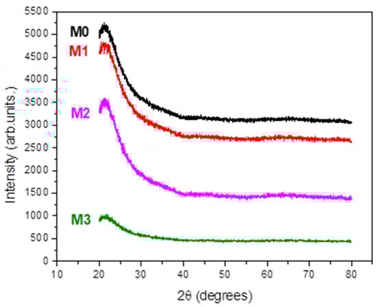
Figure 1.
XRD patterns of the studied films.
3.2. X-ray Photoelectron Spectroscopy
The XPS measurements were carried out in order to reveal the elemental composition of the films surface. Table 2 shows the binding energy and area of the peaks obtained after the gaussian deconvolution of XPS high-resolution spectra of zirconium, magnesium and oxygen corresponding to Zr 3d, Mg 3p3/2 and O 1s curves, respectively.
Table 2.
The binding energy, BE (eV), and the area (A) of the peaks Zr 3d5/2, Zr 3d3/2, O 1s, Mg 2p3/2 and C 1s.
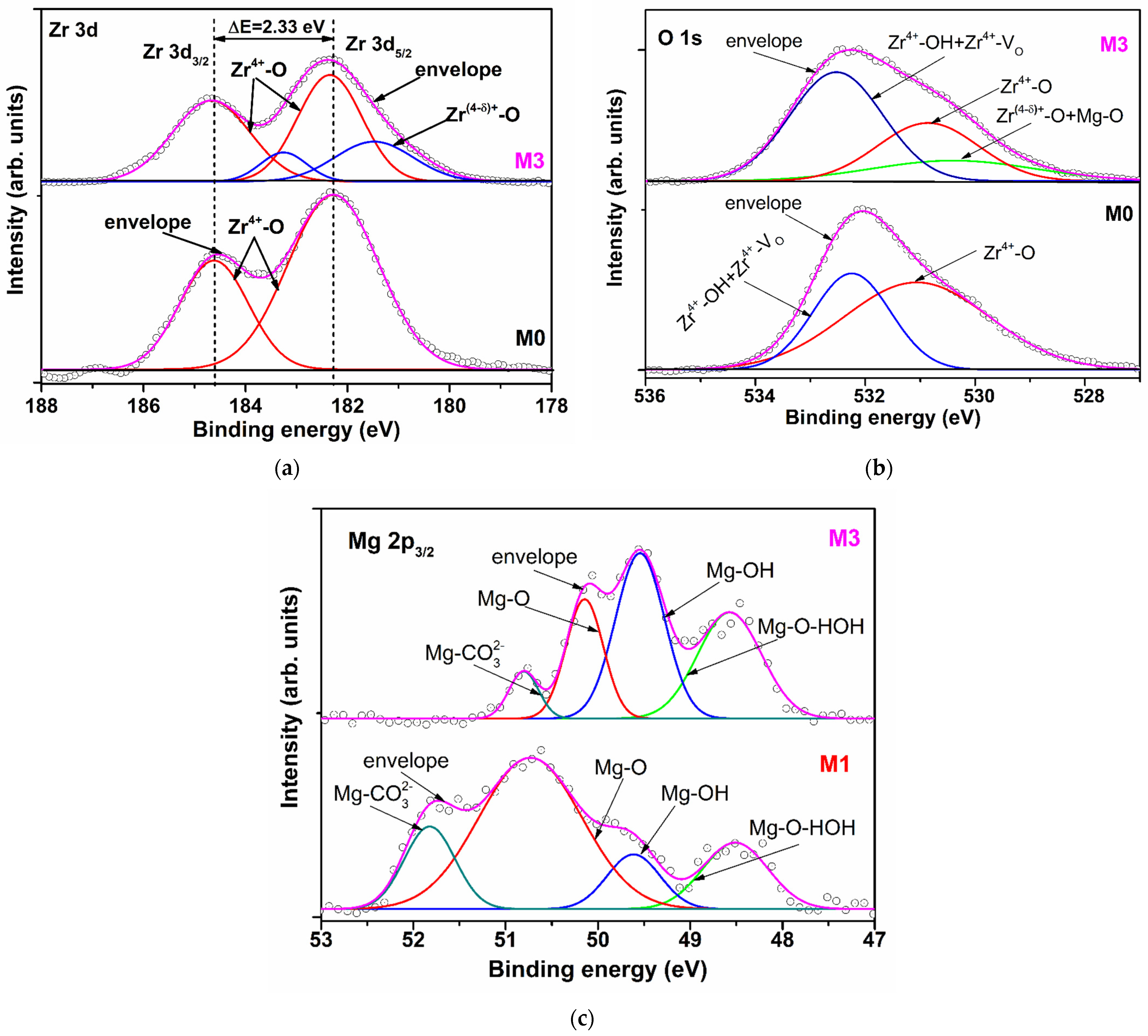
The Zr 3d XPS high-resolution spectra of M0 sample was split in two peaks located at 182.28 eV and 184.61 eV, assigned to Zr 3d5/2 and Zr 3d3/2, respectively (Figure 2a) [12]. For the Mg-doped films, besides the main peaks, lower binding energies were identified (Table 2, Figure 2a). This split of peaks can be due to the shake-up state of Zr 3d orbital determined by the increase of zirconium cation electronic density in the certain direction as a consequence of the increase of disorder degree in the structure of the film surface. The disorder is induced by the random substitution of Zr4+ by a cation with half ionic charge (Mg2+), but with the same radii (r = 0.072 nm for the coordination number C.N. = 6 and r = 0.066 nm for C.N. = 5 [13]), which may create anionic disorder expressed by increasing of non-equivalent oxygen environments and oxygen vacancies, respectively. The incorporation of magnesium cations in the zirconia matrix (M0) induced a shift of the Zr 3d5/2 and Zr 3d3/2 main peaks binding energies to higher values for the film M1, and a shift to lower values for M2, and M3. So, the decrease is from 182.65 eV (M1) to 182.12 eV (M3) and from 184.97 eV (M1) to 184.45 eV (M3), respectively (Table 2). The same tendency was observed for the lower binding energy peaks Zr 3d5/2: from 181.58 eV (M1) to 181.27 eV (M3). These progressive decrease of positively core shell level of Zr4+ (design as Zr(4-δ)+ in Figure 2a) with the doping level can be attributed to the temporarily capturing of one electron and therefore an increase of the compensation effect of negatively charge reduction [14] and/or to the presence of oxygen species associated with smaller charge negatively contribution (HO−,O2−) [15,16]. The spin-orbit splitting of Zr 3d5/2 and Zr 3d3/2 core levels around 2.30 eV suggests that the maximum oxidation state of zirconium is conserved but with an enhanced contribution of oxygen species with lower negative charge. The above observations are confirmed by the increase of Zr(4-δ)+-O bonds total contribution from 4.52% for M1 to 24.45% for M3.
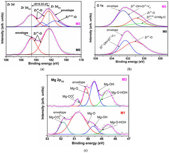
Figure 2.
High-resolution spectra and peak fitting of (a) Zr 3d and (b) O 1s for M0 and M3 and (c) Mg 2p3/2 for M1 and M3.
The binding energy components of O 1s for the under-study films are presented in Table 2 and for M0 and M3 are depicted in Figure 2b. They consist in two peaks for M0 and M1 and three peaks for M2 and M3. The peaks located at 531.06 eV (M0), 530.44 eV (M1), 530.65 eV (M3) and 530. 86 eV (M3) were assigned to Zr4+-O lattice. The peaks centered at 529.62 eV, 529.62 eV (M2) and 530.40 eV (M3) were attributed to Zr(4-δ)+-O and Mg2+-O bonds [17], having a contribution of about 2%, 3% and 16%, respectively from the total area of O1s peaks. The much higher contribution of Zr(4-δ)+-O and Mg2+-O bonds could be attributed to an increased concentration of Mg2+ on the M3 surface despite the lack of difference between Zr4+ and Mg2+ atomic radii (for the same C.N.). This will induce the supplementary oxygen vacancies which will favour the water molecules adsorption. The binding energy assigned to Zr-OH and Zr-VO bonds (where VO is oxygen vacancy) (about 532 eV—Table 2) and the contribution of the second O 1s peak for M0 (36.94%) and the third peaks for M1–M3 (49.60%, 52.39% and 63.40% respectively) confirm the above statement. The slightly increase of the binding energy with magnesium doping level can be attributed to an increase of OH groups contribution against VO concentration.
XPS high-resolution spectra of Mg 2p3/2 of the films M1 and M2 are larger than for the film M3. The Mg 2p3/2 signal can be fitted in four components for all the doped films. The binding energies and the corresponding peak areas are presented in Table 2 and Figure 2c for M1 and M3 films. The peaks located at 48.51 eV (M1), 48.30 eV (M2) and 48.57 eV (M3) we assigned to Mg-O-HOH (water) bonds which have a less covalent character than Mg-OH bonds because the obtained method of under study films didn’t facilitate the reduction of Mg2+ to Mg0 [18]. The second peaks, centered at 49.61 eV (M1), 49.61 eV (M2) and 49.54 eV (M3), having 10.74%, 26.50% and 38.99% contribution, respectively, correspond to the Mg-OH groups. 1 eV differences between the Mg-O-HOH (water) and Mg-OH bonds confirm the inhomogeneous charging of these two bonds. The cumulative contribution of Mg-O-HOH (water) and Mg-OH bonds show that the most adsorptive centers of the lattice are located on/or next to the manganese atoms.
Higher binding energy of peaks located at 50.73 and 50.82 eV (M1), 50.03 and 50.14 eV (M2), 50.14 and 50.80 eV (M3) were associated with Mg-O and Mg-CO32− bonds, respectively. The presence of CO32− ions are confirmed by the C 1s peaks located at about 286 eV (Table 2). The Mg-O/Mg-CO32− contribution bonds ratio increases with doping level from 3.25 for M1 to 5.63 for M3, which indicates that the CO2 quantity adsorbed on the film surfaces don’t dominate adsorption process, suggesting that HO groups are the main factor which influences the conduction properties of the Mg doped zirconia films.
3.3. Optical Band Gap
While passing through a material, the light intensity decreases due to two phenomena: absorption and scattering. In the energy domain where the fundamental absorption of light is the dominant phenomena, the absorption coefficient () at a certain wavelength is given by the relation [19]:
where T is the measured optical transmittance at the same wavelength and d is the thickness of the film. According to the literature [11], we assume that in the neighborhood of the fundamental absorption of ZrO2, direct allowed transitions are dominant and the dependence α(hν), is given by the relation [2]:
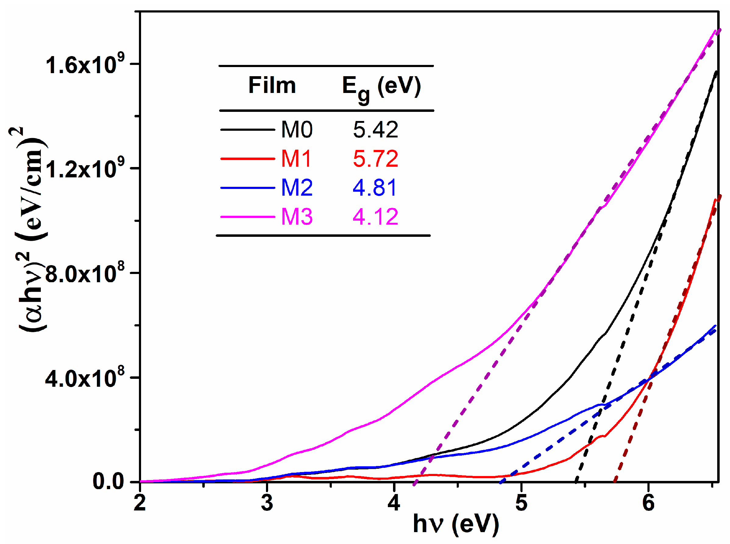
where Eg is the optical band gap energy and B is a constant which does not depend on energy. The values of Eg were obtained by extrapolating the linear part of the dependence to . From Figure 3, one can observe that the optical band gap decreases with Mg content, which could be important in some applications, like photocatalysis, were the light from the sun can be efficiently used. These values are consisted with those reported in literature [14], being suggested that Mg dopant determine an alteration of the electronic states between the two allowed bands (conduction band and valence band).

Figure 3.
vs. plots; determination of the optical band gap values for the studied films.
3.4. Electrical Conductivity
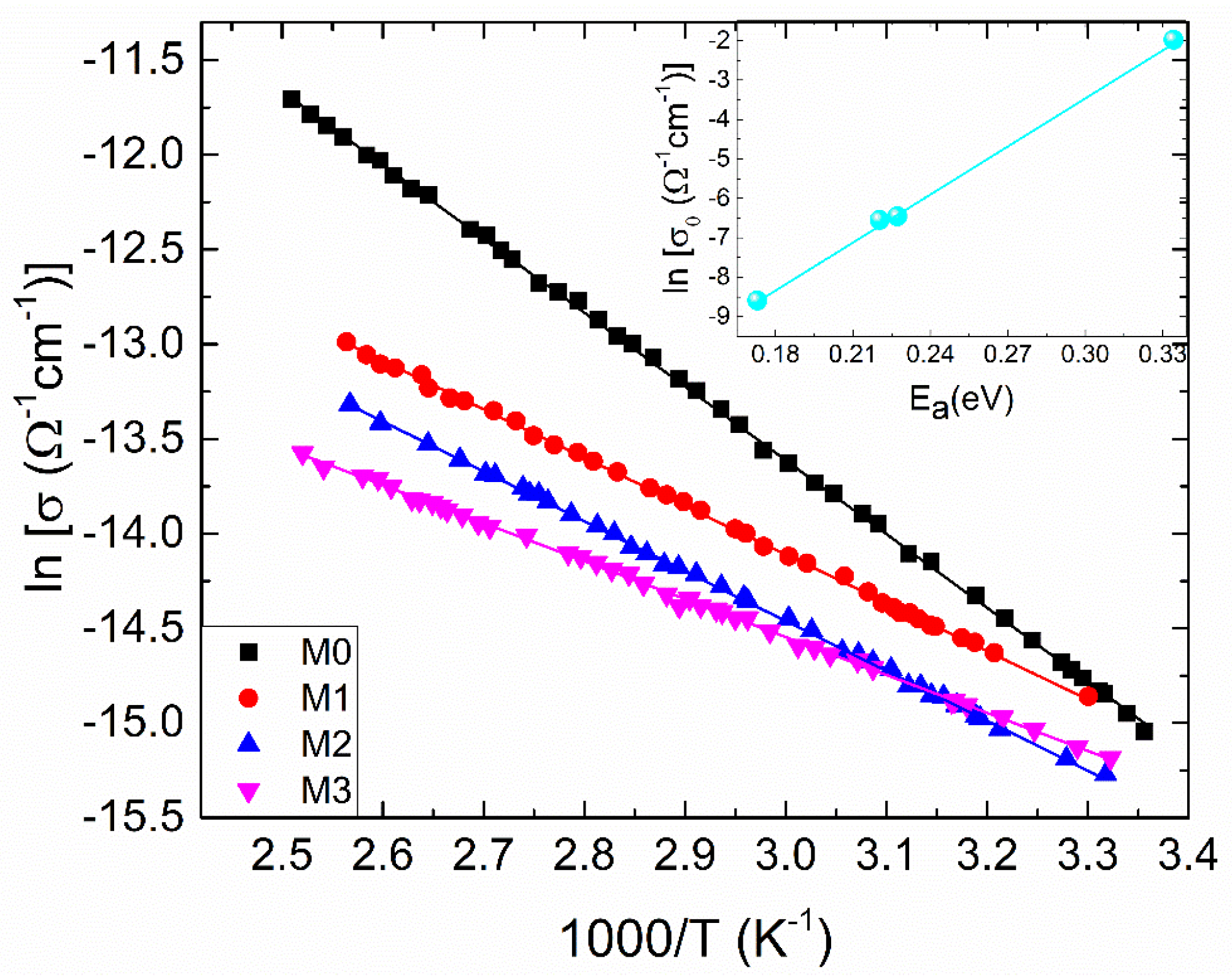
As presented in Figure 4, temperature-dependent electrical conductivities (σ) are assessed to explore the electrical conduction mechanism of zirconia and Mg-doped zirconia films. It can be observed that the dependences show typical semiconductor behavior (dσ/dT > 0) and the conductivity of ZrO2 decreases once Mg dopant enters its lattice. There are different explanations for this decrease, for different experimental conditions: Deng et al. [20] reported the electrical conductivity of ZrO2 at temperatures higher than 1000 °C which increases firstly with dopant content, reaches a maximum at a certain value of Mg dopant, and then declines with rising dopant concentration of Mg. They stated that the conductivity for Mg doped ZrO2 samples decreases because of the deterioration of the cubic solid solution and the binding between the dopant cation and the oxygen vacancy, which was found to have a substantial impact on the conductivity. Vijayakumar et al. [21] noticed that the variations in charge carrier concentration with Mg dopant in ZrO2 samples affects the conductivity. At 18 mol% Mg-ZrO2, the conductivity declines compared to the undoped ZrO2 sample. Mbae et al. [22] studied the band structure of undoped and Mg-doped ZrO2, clearly demonstrating a shift in the Fermi level towards the valence band for the doped sample, with an important role in conductivity. The shift was explained by charge compensation, since a Zr4+ ion has been replaced by a dopant with an oxidation state of +2. Yoon et al. [8] attributed the conductivity degrading by Mg doping to the increase in defect association (dopant–vacancy interaction), which reduces the vacancy mobility. Renuka et al. [6] reported that Mg dopant causes a decline in crystal quality of ZrO2 with lowering crystallite size. In this case, grain boundaries can become operative, trapping the carries and decreasing the conductivity.
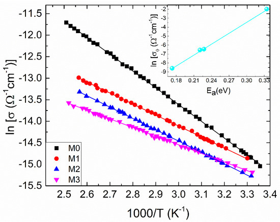
Figure 4.
The temperature dependent electrical conductivity for the samples under investigation, plotted as ln (σ) versus 1000/T. With respect to Equation (3), solid lines represent the best-fit lines. Preexponential factor (σ0) and activation energy (Ea) relationship is shown in the inset; the solid line is the best-fit line with Equation (4).
In this paper, the decrease in the electrical conductivity of ZrO2 by Mg doping was correlated with the increasing concentration of the hydroxyl groups evidenced from XPS. So, even the oxygen vacancies concentration increases by doping, due to charge compensation, these were filled by the species generated of dissociative chemisorption of ambient atmosphere water molecules (75% relative humidity).
In amorphous semiconductors, the Mott variable-range hopping (VRH) model fits well to explain the conduction process at sufficiently low temperatures, which are typically lower than room temperature [23,24,25]. In the VRH regime, carrier transport is dominated by hopping between defect states that are relatively close to the Fermi level [23,24,25]. On the other hand, the carrier transport can be explained by the Arrhenius model at higher temperatures.
Commonly for a semiconductor, its electrical conductivity, σ, can be thermally activated, being well described by the Arrhenius relation [26] given below:
where σo, Ea, kB and T denote the pre-exponential factor, thermal activation energy, Boltzmann’s constant and absolute temperature, respectively. The dependence (3) is sustained for the investigated films, since there is a linear dependence of lnσ as a function of inverse temperature (Figure 4). The inset in Figure 4 represents the dependence of ln σo versus Ea, parameters determined from the linear fitting. Accordingly, it is quite clear from the figure that there is a linear relationship between these parameters, which can be expressed by [27]:
The correlation between σo and Ea is called the Meyer-Neldel rule [27]. Here, σoo and EMN denote the MNR pre-exponential factor and the MNR characteristic energy, respectively.
The origin of MNR, mainly ascribed to the disorder or distortion in the lattice [27,28], still remains not clear. This rule was previously reported for various disordered material systems [28,29,30,31]. For instance, the explanation of the MNR observed in the electrical conductivity of CdS films, given by Hariech et al. in [31], was correlated with the disorder in the films’ matrices and with the contribution of localized states in the electrical transport. Kumar et al. reached to the same conclusion for the investigated glassy alloys Se75In25-xPbx thin films [28]. Hariech et al. consider that, even if MNR is attributed to the disorder effect in a material, its origin is connected to the dominant transport mechanism [31]. In Ref [32] Jakson et al. report that MNR could be also a consequence of the multi-trapping transport process. It is worth saying that, as far as we know, the finding of the Meyer-Neldel rule in ZrO2 thin films, is obtained here for the first time in the literature.
To elucidate the electrical conduction mechanism in the investigated films, we have carried out a thorough investigation based on MNR. By substituting σo from Equation (4) into Equation (3), one can find:
This yields a single crossing point, at a certain temperature, for various values of Ea. This temperature is known as the MNR temperature (TMN), being estimated as:
It is important to observe that at TMN, σ becomes independent of Ea. The values of σoo, EMN and TMN are found to be: 1.61 × 10⁻⁷ (cm)−1, 24.62 meV and 285.5 K, respectively. These values fall within the ranges reported for various disordered materials [26,28].
It is evident from the MNR analysis that , where is the Debye temperature previously reported between 564–575 K for ZrO2 [33,34]. Since , one can expect that the small-polaron hopping (SPH) conduction is the dominant conduction mechanism in the investigated samples [35]. Small polarons are quasiparticles made up of a charge carrier and a related lattice deformation. Because of the strong carrier-phonon coupling, carriers can frequently self-trap to form small polarons. Small polaron have substantially detrimental effect on the performance of material in various applications. Small polarons are obviously destructive for photovoltaics since they significantly reduce charge-carrier mobilities, cause charge-carrier self-trapping and carrier recombination [36]. However, small polarons could be highly useful for solid-state lighting and gamma-ray detection [37,38]. Therefore, it should be addressed for Mg-doped ZrO2.
The SPH mainly occurs in either adiabatic or nonadiabatic regime. These regimes can be identified by the possibility for the polaron to jump to the adjacent site. This possibility is high and low, for the adiabatic and nonadiabatic regime, respectively.
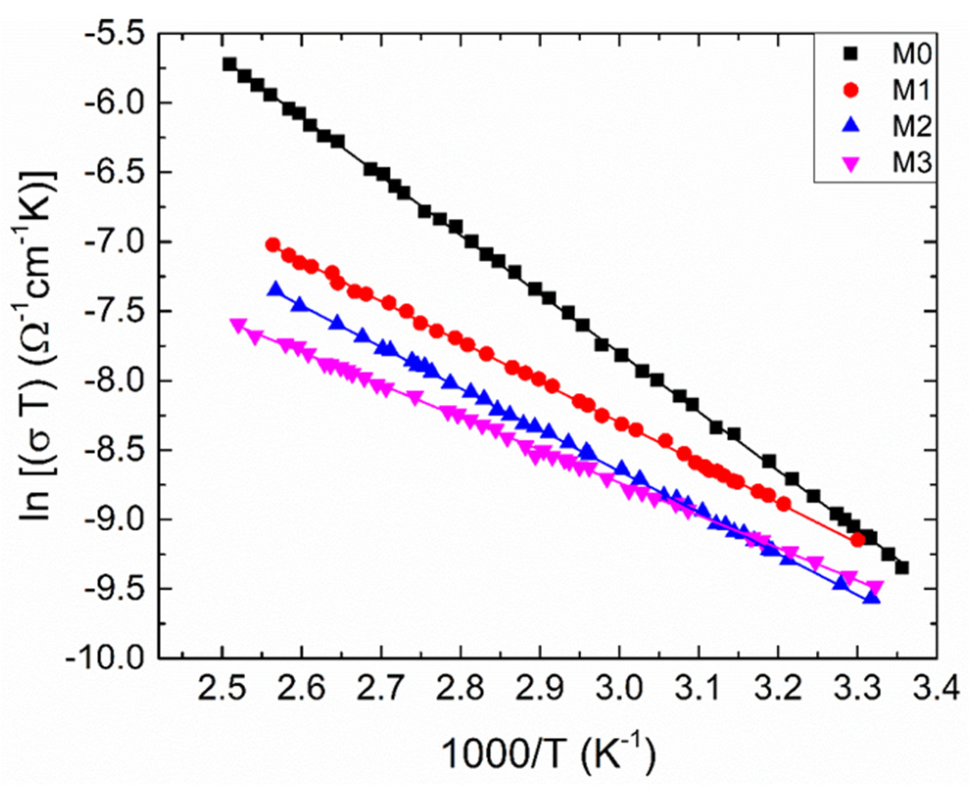
To clarify the nature of the SPH, we have to plot the dependence ln (σT) versus 1000/T (Figure 5), this dependence being well-suited to explain the SPH. Then we can reveal the charge-transfer processes in both the adiabatic and non-adiabatic conditions.
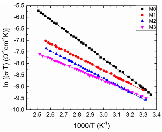
Figure 5.
The temperature dependent electrical conductivity for the samples under investigation as ln (T) versus 1000/T. Solid lines are calculated by utilizing the least-squares technique.
In the frame of the SPH model, the electrical conductivity in the non-adiabatic regime is given as [39]:
where p is:
In the relations (7) and (8), and Ep denote the pre-exponential factor and the activation energy, respectively; is the optical phonon frequency, being about 1013 Hz; C and R stand for the fraction of transition metal ions and the average distance between the ions, respectively. Herein, the value of C can be estimated from the measurement of temperature dependent Seebeck coefficient [40]; corresponds to the inverse of location length; e is the electron charge; kB is the Boltzmann’s constant. In the adiabatic regime, approaches to 1. We fitted the measured data with Equation (7) (Figure 5). The estimated values of Ep are listed in Table 3. Knowing Ep values, one can obtain the polaron hopping energy (). In these equations, . where is the polaron radius. The following equations can be considered:
and
where is the effective dielectric constant, (=4.6) and (=21) are the high and static dielectric constants of ZrO2, respectively [41]. Then, we can derive the polaron hopping energy, , defined as:
We can also calculate the disorder energy (Ed), defined as:
The energy Ep consists of these energies for , expressed as:
Note that these values tabulated in Table 3 are in a good agreement with those reported in the literature [40,41,42,43,44].
Table 3.
The electrical parameters of the studied films.
The possibility of polaron hopping is proportional to the transfer integral (J) given as [43]:
We calculated the value of J to be as 28.7 meV at 330 K. If the value of J is big enough, adiabatic regime is operative. Otherwise, non-adiabatic regime becomes important. Considering a relationship reflecting how high hopping possibility is, one can distinguish between adiabatic and non-adiabatic regimes. To do so, the value of J should be compared to H expressed by the following relation [45]:
If J > H, hopping takes place in adiabatic regime, while hopping occurs in non-adiabatic regime when J < H. The values of estimated H are given in Table 3. So, one can see that the polaron travels via the non-adiabatic hopping regime in the films under study. To determine the value of the SPH coupling constant (), which indicates how strong the carrier-phonon interaction is, one can use the relation [39]:
Since is higher than 4 for all the samples, it confirms that a strong carrier-phonon interaction happens in the samples and carrier transport is associated with SPH mechanism. Finally, the samples should fulfil the condition of SPH model given below [39]:
The condition is satisfied with all the samples, confirming the applicability of SPH model to the samples.
4. Conclusions
In this paper, we have reported on the electrical conduction mechanism of amorphous Mg-doped ZrO2 thin films, deposited by dip coating. A detailed XPS analysis was performed. The optical band gap, obtained from optical transmittance spectra, decreases by Mg doping, from 5.42 eV to 4.12 eV. By studying the dependence of the electrical conductivity as a function of temperature, a characteristic semiconductor behavior is observed. The decrease of the conductivity once Mg enters of ZrO2 lattice was related to the increase of the hydroxyl groups evidenced by XPS. It was shown that the electrical conductivity follows the Meyer-Neldel rule (reported here for ZrO2 for the first time in the literature), with the parameters σoo, EMN and TMN having values that falls in domains reported for various disordered materials: 1.61 × 10⁻⁷ (Ω cm)−1, 24.62 meV and 285.5 K, respectively. The Meyer-Neldel rule, even largely accepted in the literature to be attributed to the disorder effect in the material, has an origin which was explained for the studied films based on small-polaron hopping model, in the non-adiabatic hopping regime.
Author Contributions
Conceptualization, D.M. and A.Y.; methodology, D.M., M.F., C.M., N.C., G.B., M.D., A.D. and A.Y.; validation, D.M., C.M., N.C. and A.Y.; formal analysis, D.M., M.F., C.M., G.B., M.D. and A.D.; investigation, D.M., M.F., C.M., G.B., M.D., A.D. and A.Y.; resources, D.M., C.M., M.F., G.B. and M.D.; data curation, D.M., M.F., C.M. and A.Y.; writing—original draft preparation, D.M., C.M., N.C. and A.Y.; writing—review and editing, D.M., C.M. and A.Y.; visualization, D.M. and A.Y.; supervision, D.M., C.M. and A.Y. All authors have read and agreed to the published version of the manuscript.
Funding
This research received no external funding.
Institutional Review Board Statement
Not applicable.
Informed Consent Statement
Not applicable.
Data Availability Statement
The original contributions presented in the study are included in the article, further inquiries can be directed to the corresponding authors.
Conflicts of Interest
The authors declare no conflicts of interest.
References
- Altalhi, T.; Gobouri, A.A.; Al-Harbi, L.M.; Refat, M.S.; El-Nahass, M.M.; Hassanien, A.M.; Atta, A.A.; Ahmed, E.M.A. Structural, diffuse reflectance spectroscopy and dielectric relaxation properties of zirconium (IV) dioxide. J. Mater. Res. Technol. 2021, 12, 1194–1202. [Google Scholar] [CrossRef]
- Lou, C.; Li, Z.; Yang, C.; Liu, X.; Zheng, W.; Zhang, J. Rational design of ordered porous SnO2/ZrO2 thin films for fast and selective triethylamine detection with humidity resistance. Sens. Actuators B Chem. 2021, 333, 129572. [Google Scholar] [CrossRef]
- Omar, S.; Najib, W.B.; Chen, W.; Bonanos, N. Electrical Conductivity of 10 mol% Sc2O3–1 mol% M2O3–ZrO2 Ceramics. J. Am. Ceram. Soc. 2012, 95, 1965–1972. [Google Scholar] [CrossRef]
- Buchanan, R.C.; Pope, S. Optical and Electrical Properties of Yttria Stabilized Zirconia (YSZ) Crystals. J. Electrochem. Soc. Solid-State Sci. Technol. 1983, 130, 962–966. [Google Scholar] [CrossRef]
- Strickler, D.W.; Carlson, W.G. Electrical Conductivity in the ZrO2 -Rich Region of Several M2O3-ZrO2 Systems. J. Am. Ceram. Soc. 1965, 48, 286–289. [Google Scholar] [CrossRef]
- Renuka, L.; Anantharaju, K.S.; Sharma, S.C.; Nagaswarupa, H.P.; Prashantha, S.C.; Nagabhushana, H.; Vidya, Y.S. Hollow microspheres Mg-doped ZrO2 nanoparticles: Green assisted synthesis and applications in photocatalysis and photoluminescence. J. Alloys Compd. 2016, 672, 609–622. [Google Scholar] [CrossRef]
- Kim, M.; Oh, S.B.; Joo, H. Conduction Mechanism in Acceptor- or Donor-Doped ZrO2 Bulk and Thin Films. ACS Appl. Mater. Interfaces 2023, 15, 31627–31634. [Google Scholar] [CrossRef] [PubMed]
- Yoon, S.; Noh, T.; Kim, W.; Choi, J. Structural parameters and oxygen ion conductivity of Y2O3–ZrO2 and MgO–ZrO2 at high temperature. Ceram. Int. 2013, 39, 9247–9251. [Google Scholar] [CrossRef]
- Joo, J.H.; Choi, G.M. Electrical conductivity of YSZ film grown by pulsed laser deposition. Solid State Ion. 2006, 177, 1053–1057. [Google Scholar] [CrossRef]
- Joo, J.H.; Choi, G.M. Electrical conductivity of scandia-stabilized zirconia thin film. Solid State Ion. 2008, 179, 1209–1213. [Google Scholar] [CrossRef]
- Moura, C.; Carvalho, P.; Vaz, F.; Cunha, L.; Alves, E. Raman spectra and structural analysis in ZrOxNy thin films. Thin Solid Film. 2006, 515, 1132–1137. [Google Scholar] [CrossRef]
- Jeong, K.S.; Song, J.; Lim, D.; Lee, M.S.; Kim, H.; Cho, M.H. Structural evolution and defect control of yttrium-doped ZrO2 films grown by a sol-gel method. Appl. Surf. Sci. 2014, 320, 128–137. [Google Scholar] [CrossRef]
- Shannon, R.D. Revised effective ionic radii and systematic studies of interatomic distances in halides and chalcogenides. Acta Cryst. 1976, A32, 751–767. [Google Scholar] [CrossRef]
- Salari, S.; Ghods, F.E. A significant enhancement in the photoluminescence emission of the Mg doped ZrO2 thin films by tailoring the effect of oxygen vacancy. J. Lumin. 2017, 182, 289–299. [Google Scholar] [CrossRef]
- Anderson, J.A.; Fierro, J.L.G. Bulk and surface properties of copper-containing oxides of the general formula LaZr1-xCuxO3. J. Solid State Chem. 1994, 108, 305–313. [Google Scholar] [CrossRef]
- Lakshmi, J.S.; Berlin, I.J.; Daniel, G.P.; Thomas, P.V.; Joy, K. Effect of calcination atmosphere on photoluminescence properties of nanocrystalline ZrO2 thin films prepared by sol–gel dip coating method. Phys. B Condens. Matter. 2011, 406, 3050–3055. [Google Scholar] [CrossRef]
- Montero, J.M.; Isaacs, M.A.; Lee, A.F.; Lynam, J.M.; Wilson, K. The surface chemistry of nanocrystalline MgO catalysts for FAME production: An in situ XPS study of H2O, CH3OH and CH3OAc adsorption. Surf. Sci. 2016, 646, 170–178. [Google Scholar] [CrossRef]
- Wanga, L.; Shinoharaa, T.; Zhang, B.-P. XPS study of the surface chemistry on AZ31 and AZ91 magnesium alloys in dilute NaCl solution. Appl. Surf. Sci. 2010, 256, 5807–5812. [Google Scholar] [CrossRef]
- Mardare, D.; Tasca, M.; Delibas, M.; Rusu, G.I. On the structural properties and optical transmittance of TiO2 R.F. sputtered thin films. Appl. Surf. Sci. 2000, 156, 200–206. [Google Scholar] [CrossRef]
- Deng, W.; Li, Y. High-temperature electrical properties of polycrystalline MgO-doped ZrO2. Mater. Res. Bull. 2019, 113, 182–189. [Google Scholar] [CrossRef]
- Vijayakumar, M.; Selvasekarapandian, S.; Bhuvaneswari, M.S.; Kumar, G.H.; Ramprasad, G.; Subramanian, R.; Angelo, P.C. Synthesis and ion dynamics studies of nanocrystalline Mg stabilized zirconia. Phys. B 2003, 334, 390–397. [Google Scholar] [CrossRef]
- Mbae, J.K.; Muthui, Z.W. Doping induced phase stabilization and electronic properties of alkaline earth metal doped zirconium (IV) oxide: A first principles study. Heliyon 2023, 9, e20998. [Google Scholar] [CrossRef] [PubMed]
- Mott, N.F. Conduction in glasses containing transition metal ions. J. Non-Cryst. Solids 1968, 1, 1–17. [Google Scholar] [CrossRef]
- Serin, T.; Yildiz, A.; Șahin, Ș.H.; Serin, N. Multiphonon hopping of carriers in CuO thin films. Phys. B 2011, 406, 3551–3555. [Google Scholar] [CrossRef]
- Serin, N.; Yildiz, A.; Alsac, A.A.; Serin, T. Estimation of compensation ratio by identifying the presence of different hopping conduction mechanisms in SnO2 thin films. Thin Solid Film. 2011, 519, 2302–2307. [Google Scholar] [CrossRef]
- Mardare, D.; Yildiz, A.; Apetrei, R.; Rambu, P.; Florea, D.; Gheorghe, N.G.; Macovei, D.; Teodorescu, C.M.; Luca, D. The Meyer-Neldel Rule in amorphous TiO2 films with different Fe content. J. Mater. Res. 2012, 27, 2271–2277. [Google Scholar] [CrossRef]
- Meyer, W.; Neldel, H. Relation between the energy constant and the quantity constant in the conductivity–temperature formula of oxide semiconductors. Z. Tech. Phys. 1937, 12, 588–593. [Google Scholar]
- Kumar, D.; Kumar, S. Pre-exponential factor in a-Se75In25-xPbx thin films. Bull. Mater. Sci. 2004, 27, 441–444. [Google Scholar] [CrossRef]
- Guillén, C.; Herrero, J. Investigations of the electrical properties of electrodeposited CuInSe2 thin films. J. Appl. Phys. 1992, 71, 5479–5483. [Google Scholar] [CrossRef]
- Morii, K.; Matsui, T.; Tsuda, H.; Mabuchi, H. Meyer–Neldel rule in amorphous strontium titanate thin films. Appl. Phys. Lett. 2000, 77, 2361–2363. [Google Scholar] [CrossRef]
- Hariech, S.; Aida, M.S.; Moualkia, H. Observation of Meyer–Neldel rule in CdS thin films. Mater. Sci. Semicond. Process. 2012, 15, 181–186. [Google Scholar] [CrossRef]
- Jakson, W.B. Connection between the Meyer-Neldel relation and multiple-trapping transport. Phys. Rev. B Condens. Matter. 1988, 38, 3595–3598. [Google Scholar] [CrossRef] [PubMed]
- Nevitt, M.V.; Fang, Y.; Chan, S.K. Heat Capacity of Monoclinic Zirconia between 2.75 and 350 K. J. Am. Ceram. Soc. 1990, 73, 2502–2504. [Google Scholar] [CrossRef]
- Cheng, Y.; Zhang, T.; Qi, Y.-Y. Elastic Properties of Monoclinic ZrO2 at Finite Temperatures Via First Principles. Int. J. Thermophys. 2014, 35, 145–153. [Google Scholar] [CrossRef]
- Kemeny, G.; Rosenberg, B. Small polarons in organic and biological semiconductors. J. Chem. Phys. 1970, 53, 3549–3551. [Google Scholar] [CrossRef]
- Zelewski, S.J.; Urban, J.M.; Surrente, A.; Maude, D.K.; Kuc, A.; Schade, L.; Johnson, R.D.; Dollmann, M.; Nayak, P.K.; Snaith, H.J.; et al. Revealing the nature of photoluminescence emission in the metal-halide double perovskite Cs2AgBiBr6. J. Mater. Chem. C 2019, 27, 8350–8356. [Google Scholar] [CrossRef]
- Smith, M.D.; Karunadasa, H.I. White-Light Emission from Layered Halide Perovskites. Acc. Chem. Res. 2018, 51, 619–627. [Google Scholar] [CrossRef] [PubMed]
- Dotzler, C.; Williams, G.V.M.; Edgar, A.; Schweizer, S.; Henke, B.; Spaeth, J.M.; Bittar, A.; Hamlin, J.; Dunford, C. The effect of X-ray, ϒ-ray, and UV radiations on the optical properties of RbCdF3: Mn2+. J. Appl. Phys. 2006, 100, 033102. [Google Scholar] [CrossRef]
- Mott, N.F.; Davis, E.A. Electronics Process in Non-Crystalline Materials, 2nd ed.; Clarendon: Oxford, UK, 1971. [Google Scholar]
- Yildiz, A.; Lisesivdin, S.B.; Kasap, M.; Mardare, D. Non-adiabatic small polaron hopping conduction in Nb-doped TiO2 thin film. Phys. B 2009, 404, 1423–1426. [Google Scholar] [CrossRef]
- Ceresoli, D.; Vanderbilt, D. Structural and dielectric properties of amorphous ZrO2 and HfO2. Phys. Rev. B 2006, 74, 125108. [Google Scholar] [CrossRef]
- Yildiz, A.; Iacomi, F.; Mardare, M. Polaron transport in TiO2 thin films. J. Appl. Phys. 2010, 108, 083701–083708. [Google Scholar] [CrossRef]
- Khan, W.; Naqvi, A.H.; Gupta, M.; Husain, S.; Kumar, R. Small polaron hopping conduction mechanism in Fe doped LaMnO3. J. Chem. Phys. 2011, 135, 054501. [Google Scholar] [CrossRef] [PubMed]
- Yildiz, A.; Lisesivdin, S.B.; Kasap, M.; Mardare, D. High temperature variable-range hopping conductivity in undoped TiO2 thin film. Optoelectron. Adv. Mater. Rapid Commun. 2007, 1, 531–533. [Google Scholar]
- Austin, I.G.; Mott, N.F. Polarons in crystalline and non-crystalline materials. Adv. Phys. 2001, 50, 757–812. [Google Scholar] [CrossRef]

Disclaimer/Publisher’s Note: The statements, opinions and data contained in all publications are solely those of the individual author(s) and contributor(s) and not of MDPI and/or the editor(s). MDPI and/or the editor(s) disclaim responsibility for any injury to people or property resulting from any ideas, methods, instructions or products referred to in the content. |
© 2024 by the authors. Licensee MDPI, Basel, Switzerland. This article is an open access article distributed under the terms and conditions of the Creative Commons Attribution (CC BY) license (https://creativecommons.org/licenses/by/4.0/).