
A Review of an Investigation of the Ultrafast Laser Processing of Brittle and Hard Materials
 ,
, 
Abstract
:1. Introduction
2. Mechanism of the Interaction between Ultrafast Laser and Brittle and Hard Materials
2.1. Absorption of Ultrafast Laser Energy
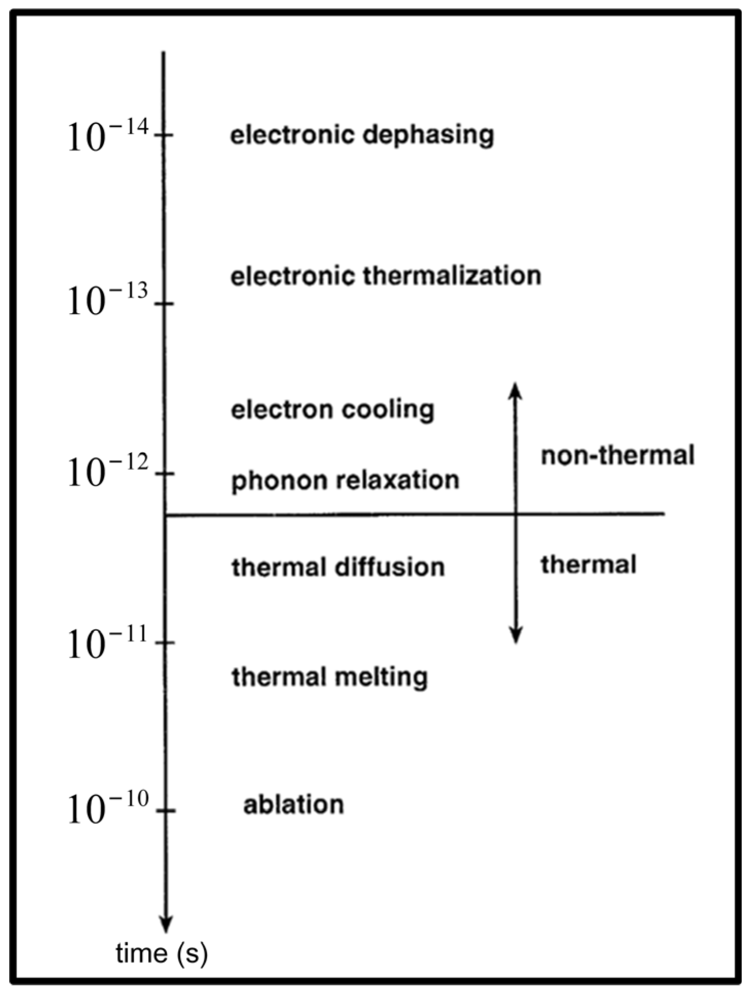
2.2. Energy Transformation
3. Ultrafast Laser Processing of Brittle and Hard Materials
3.1. Nickel-Based Superalloys and Thermal Barrier Ceramics
3.2. Diamond
3.3. SiO2 and Silica Glass
3.4. SiC and Composites
4. Precise Manufacturing of Ultrafast Laser Processing
4.1. Processing Quality Control
4.2. Precise Manufacturing System
4.3. Artificial Intelligence-Assisted Manufacturing
5. Conclusions and Perspective
- (1)
- The nonlinear laser energy absorption mechanisms of brittle and hard materials with different physical properties are still unclear. An in situ monitoring system with a high spatiotemporal resolution could be established by integrating spectral detection and three-dimensional ultrafast continuous imaging into an SEM system in order to analyze the evolution of laser-induced plasma and the absorption process of the femtosecond laser energy.
- (2)
- The coupling mechanism of laser energy transfer and the transformation of brittle and hard materials is still uncertain. Based on time-dependent density functional theory, molecular dynamics theory, and continuum theory, a multi-scale theoretical model of femtosecond laser machining could be established to carry out dynamic simulations of femtosecond laser processing. Meanwhile, combined with the above-mentioned in situ monitoring system, the evolution process of laser-induced plasma, three-dimensional morphology, and material state changes could be obtained to examine the non-equilibrium energy transfer and transformation mechanisms involved in the femtosecond laser cross-scale processing of the photon–electron–ion continuum.
- (3)
- The processing dimensional accuracy and shape accuracy of brittle and hard materials when using a femtosecond laser still need to be improved. The flexibility and stability control of laser energy parameters, such as pulse energy, pulse width, and focus position, is key to realizing high-precision femtosecond laser processing. Coordinated regulation based on the time, space, and frequency domains of femtosecond laser processing is a promising method for controlling laser energy parameters.
- (4)
- Ensuring quality consistency in the large-format femtosecond laser processing of brittle and hard materials is also a challenge. Real-time adjustments of a laser beam’s motion parameters, such as incident angle, trajectory, attitude, speed, etc., are essential to ensure consistent quality. With the integration of high-precision motion platforms, process monitoring systems, and interpolation algorithms relating to geometry, pose, and velocity, the motion parameters of the laser beam could be effectively controlled to acquire accurate processing paths, speeds, and attitudes relating to femtosecond laser processing and achieve high consistency.
- (5)
- Artificial intelligence-assisted ultrafast laser manufacturing needs to be considered. Artificial intelligence technologies, such as neural networks, machine learning, deep learning, and reinforcement learning, have good application potential in terms of establishing the relationship between process parameters and quality, as well as the intelligent planning of process parameters and the robust online optimization of process parameters in the ultrafast laser processing of brittle and hard materials. Artificial intelligence-assisted manufacturing would save a lot of time and money, be beneficial to the final properties, and improve processing efficiency and quality.
Author Contributions
Funding
Acknowledgments
Conflicts of Interest
References
- Treacy, E.B. Optical Pulse Compression with Diffraction Gratings. IEEE J. Quantum Electron. 1969, 5, 454–458. [Google Scholar] [CrossRef]
- Martinez, O.E. 3000 times grating compressor with positive group velocity dispersion: Application to fiber compensation in 1.3–1.6 μm region. IEEE J. Quantum Electron. 1987, 23, 59–64. [Google Scholar] [CrossRef]
- Li, H.; Macarthur, J.; Littleton, S.; Dunne, M.; Huang, Z.; Zhu, D. Femtosecond-Terawatt Hard X-Ray Pulse Generation with Chirped Pulse Amplification on a Free Electron Laser. Phys. Rev. Lett. 2022, 129, 213901. [Google Scholar] [CrossRef] [PubMed]
- Kappe, F.; Karli, Y.; Wilbur, G.; Krämer, R.G.; Ghosh, S.; Schwarz, R.; Kaiser, M.; Bracht, T.K.; Reiter, D.E.; Nolte, S.; et al. Chirped Pulses Meet Quantum Dots: Innovations, Challenges, and Future Perspectives. Adv. Quantum Technol. 2024, 7, 2300352. [Google Scholar] [CrossRef]
- Yamaizumi, K.; Hondo, F.; Fuji, T. Chirped pulse amplification based on praseodymium-doped fluoride fibers. Opt. Express 2023, 31, 16127–16132. [Google Scholar] [CrossRef]
- Koenig, K. Medical femtosecond laser. J. Eur. Opt. Soc. Rapid Publ. 2023, 19, 36. [Google Scholar] [CrossRef]
- Yao, Y.; Ge, Z.; Chen, Q.; Tang, J.; Zhang, Y. Surface Characteristics of Medical Zr-Based Bulk Metallic Glass Processed by Femtosecond Laser. Laser Optoelectron. Prog. 2020, 57, 111409. [Google Scholar]
- Muhammad, N.; Li, L. Underwater femtosecond laser micromachining of thin nitinol tubes for medical coronary stent manufacture. Appl. Phys. A Mater. Sci. Process. 2012, 107, 849–861. [Google Scholar] [CrossRef]
- Hoenninger, C.; Ploetner, M.; Ortac, B.; Ackermann, R.; Kammel, R.; Limpert, J.; Nolte, S.; Tuennermann, A. Femtosecond fiber laser system for medical applications. In Commercial and Biomedical Applications of Ultrafast Lasers IX; Neev, J., Nolte, S., Heisterkamp, A., Trebino, R., Eds.; SPIE: Bellingham, WA, USA, 2009; Volume 7203. [Google Scholar]
- Qian, W.; Cai, J.; Xin, Z.; Ye, Y.; Dai, F.; Hua, Y. Femtosecond laser polishing with high pulse frequency for improving performance of specialised aerospace material systems: MCrAlY coatings in thermal barrier coating system. Int. J. Mach. Tools Manuf. 2022, 182, 103954. [Google Scholar] [CrossRef]
- Helie, D.; Lacroix, F.; Vallee, R. Bonding of Optical Materials by Femtosecond Laser Welding for Aerospace and High Power Laser Applications. In Photonics North 2012; SPIE: Bellingham, WA, USA, 2012; Volume 8412. [Google Scholar]
- Xu, S.; Zhang, Y.; Wang, T.; Zhang, L. Recent Developments of Femtosecond Laser Direct Writing for Meta-Optics. Nanomaterials 2023, 13, 1623. [Google Scholar] [CrossRef]
- Liu, F.; Li, P.; Liu, S.; Jin, C.; Wei, B.; Min, J.; Liu, Z.; Zhu, X.; Zhao, J. Phase-type diffractive micro-optics elements in sulfur-based polymeric glass by femtosecond laser direct writing. Opt. Lett. 2023, 48, 1056–1059. [Google Scholar] [CrossRef] [PubMed]
- Semaltianos, N.G.; Perrie, W.; French, P.; Sharp, M.; Dearden, G.; Logothetidis, S.; Watkins, K.G. Femtosecond laser ablation characteristics of nickel-based superalloy C263. Appl. Phys. A-Mater. Sci. Process. 2009, 94, 999–1009. [Google Scholar] [CrossRef]
- Das, D.K.; Pollock, T.M. Femtosecond laser machining of cooling holes in thermal barrier coated CMSX4 superalloy. J. Mater. Process. Technol. 2009, 209, 5661–5668. [Google Scholar] [CrossRef]
- Ma, S.; McDonald, J.P.; Tryon, B.; Yalisove, S.M.; Pollock, T.M. Femtosecond laser ablation regimes in a single-crystal superalloy. Metall. Mater. Trans. A-Phys. Metall. Mater. Sci. 2007, 38A, 2349–2357. [Google Scholar] [CrossRef]
- Feng, Q.; Picard, Y.N.; Liu, H.; Yalisove, S.M.; Mourou, G.; Pollock, T.M. Femtosecond laser micromachining of a single-crystal superalloy. Scr. Mater. 2005, 53, 511–516. [Google Scholar] [CrossRef]
- Das, D.K.; McDonald, J.P.; Yallsove, S.M.; Pollock, T.M. Depth-profiling study of a thermal barrier coated superalloy using femtosecond laser-induced breakdown spectroscopy. Spectrochim. Acta Part B-At. Spectrosc. 2008, 63, 27–36. [Google Scholar] [CrossRef]
- Feng, Q.; Picard, Y.N.; Liu, H.; Yalisove, S.M.; Mourou, G.; Pollock, T.M. Femtosecond laser micromachining of single-crystal superalloys. In Proceedings of the Symposium on Solidification Processes and Microstructures in Honor of Wilfried Kurz held at the TMS Annual Meeting, Charlotte, NC, USA, 14–18 March 2004; pp. 345–346. [Google Scholar]
- Kuzmin, E.V.; Krasin, G.K.; Gulina, Y.S.; Danilov, P.A.; Pomazkin, D.A.; Gorevoy, A.V.; Kuznetsov, S.V.; Voronov, V.V.; Kovalev, V.U.; Kudryashov, S.I.; et al. Structural Micromodification of Diamond by Femtosecond Laser Pulses through Optical Contact with a Nonlinear Highly Refractive Immersion Medium. JETP Lett. 2024, 119, 280–284. [Google Scholar] [CrossRef]
- Wang, H.; Wen, Q.; Huang, H.; Huang, G.; Jiang, F.; Lu, J.; Wu, X. Ablation Characteristics and Material Removal Mechanism of CVD Single Crystal Diamond Under Femtosecond Laser Irradiation. Acta Photonica Sin. 2023, 52, 22714–22731. [Google Scholar]
- Rimskaya, E.; Kriulina, G.; Kuzmin, E.; Kudryashov, S.; Danilov, P.; Kirichenko, A.; Rodionov, N.; Khmelnitskii, R.; Chen, J. Interactions of Atomistic Nitrogen Optical Centers during Bulk Femtosecond Laser Micromarking of Natural Diamond. Photonics 2023, 10, 135. [Google Scholar] [CrossRef]
- Kononenko, V.V. Modification of Diamond Surface by Femtosecond Laser Pulses. Photonics 2023, 10, 1077. [Google Scholar] [CrossRef]
- De Michele, V.; Marin, E.; Boukenter, A.; Cannas, M.; Girard, S.; Ouerdane, Y. Photoluminescence of Point Defects in Silicon Dioxide by Femtosecond Laser Exposure. Phys. Status Solidi A-Appl. Mater. Sci. 2021, 218, 2000802. [Google Scholar] [CrossRef]
- Zheng, Q.; Jiang, G.; Cui, J.; Fan, Z.; Sun, Z.; Mei, X. Influence of Pulse Energy and Scanning Speed of Femtosecond Laser on Surface Roughness of SiC Ceramics. Integr. Ferroelectr. 2021, 219, 20–27. [Google Scholar] [CrossRef]
- Zheng, Q.; Cui, J.; Fan, Z.; Yan, Z.; Lin, Q.; Jiang, G.; Mei, X. Investigation on the underwater femtosecond laser polishing SiC ceramic. Ferroelectrics 2020, 564, 28–36. [Google Scholar] [CrossRef]
- Zheng, Q.; Cui, J.; Fan, Z.; Mei, X. An experimental investigation of scan trajectory into the underwater femtosecond laser polishing SiC ceramic. Ferroelectrics 2020, 563, 77–86. [Google Scholar] [CrossRef]
- Zheng, Q.; Fan, Z.; Jiang, G.; Pan, A.; Yan, Z.; Lin, Q.; Cui, J.; Wang, W.; Mei, X. Mechanism and morphology control of underwater femtosecond laser microgrooving of silicon carbide ceramics. Opt. Express 2019, 27, 26264–26280. [Google Scholar] [CrossRef]
- Soltani, B.; Azarhoushang, B.; Zahedi, A. Laser ablation mechanism of silicon nitride with nanosecond and picosecond lasers. Opt. Laser Technol. 2019, 119, 105644. [Google Scholar] [CrossRef]
- Chen, M.; Wang, X.; Qi, D.; Deng, H.; Liu, Y.; Shen, X. Temperature field simulation of chalcogenide glass ablation by nanosecond pulsed laser-based on pump-probe technology. Opt. Laser Technol. 2022, 149, 107771. [Google Scholar] [CrossRef]
- Yan, Z.; Mei, X.; Wang, W.; Pan, A.; Lin, Q.; Huang, C. Numerical simulation on nanosecond laser ablation of titanium considering plasma shield and evaporation-affected surface thermocapillary convection. Opt. Commun. 2019, 453, 124384. [Google Scholar] [CrossRef]
- Volkov, A.N.; Lin, Z. Anomalously strong effects of plume contraction and material redeposition in nanosecond pulsed laser vaporization. Int. J. Heat Mass Transf. 2023, 216, 124511. [Google Scholar] [CrossRef]
- Peng, Z.; Yin, J.; Cui, Y.; Cao, Y.; Lu, L.; Yan, Y.; Hu, Z. Numerical and experimental investigation on pulsed nanosecond laser ablation processing of aluminum alloy. J. Mater. Res. Technol. 2022, 19, 4708–4720. [Google Scholar] [CrossRef]
- Cha, D.; Axinte, D. Transient thermal model of nanosecond pulsed laser ablation: Effect of heat accumulation during processing of semi-transparent ceramics. Int. J. Heat Mass Transf. 2021, 173, 121227. [Google Scholar] [CrossRef]
- Leong, C.Y.; Yap, S.S.; Ong, G.L.; Ong, T.S.; Yap, S.L.; Chin, Y.T.; Foon Lee, S.; Tou, T.Y.; Nee, C.H. Single pulse laser removal of indium tin oxide film on glass and polyethylene terephthalate by nanosecond and femtosecond laser. Nanotechnol. Rev. 2020, 9, 1539–1549. [Google Scholar] [CrossRef]
- Pan, A.; Mei, X.; Wang, W.; Xia, Y.; Su, Y.-Q.; Zhao, S.; Chen, T. In-situ deposition of oxidized porous metal nanoparticles on the surface of picosecond laser-induced micro/nano structures: A new kind of meta-surface equipped with both super-hydrophobicity and anti-reflectivity. Chem. Eng. J. 2023, 460, 141582. [Google Scholar] [CrossRef]
- Barbato, P.; Osellame, R.; Martinez Vazquez, R. Femtosecond Laser Nanomachining of High-Aspect-Ratio Channels in Bulk Fused Silica. Adv. Mater. Technol. 2024, 9, 2400240. [Google Scholar] [CrossRef]
- Petronic, S.; Drecun-Nesic, S.; Milosavljevic, A.; Sedmak, A.; Popovic, M.; Kovacevic, A. Microstructure Changes of Nickel-Base Superalloys Induced by Interaction with Femtosecond Laser Beam. Acta Phys. Pol. A 2009, 116, 550–552. [Google Scholar] [CrossRef]
- Keldysh, L.V. Ionization in the field of a strong electromagnetic wave. Sov. Phys. Jetp. 1965, 20, 1307–1315. [Google Scholar]
- Stuart, B.C.; Feit, M.D.; Herman, S.; Rubenchik, A.M.; Shore, B.W.; Perry, M.D. Nanosecond-to-femtosecond laser-induced breakdown in dielectrics. Phys. Rev. B 1996, 53, 1749–1761. [Google Scholar] [CrossRef] [PubMed]
- Schaffer, C.B.; Brodeur, A.; Mazur, E. Laser-induced breakdown and damage in bulk transparent materials induced by tightly focused femtosecond laser pulses. Meas. Sci. Technol. 2001, 12, 1784–1794. [Google Scholar] [CrossRef]
- Gattass, R.R.; Mazur, E. Femtosecond laser micromachining in transparent materials. Nat. Photonics 2008, 2, 219–225. [Google Scholar] [CrossRef]
- Eaton, S.M.; Cerullo, G.; Osellame, R. Fundamentals of Femtosecond Laser Modification of Bulk Dielectrics; Springer: Berlin/Heidelberg, Germany, 2012; pp. 3–18. [Google Scholar]
- Sugioka, K.; Cheng, Y. Femtosecond laser three-dimensional micro- and nanofabrication. Appl. Phys. Rev. 2014, 1, 041303. [Google Scholar] [CrossRef]
- Huang, Q.; Yin, K.; Wang, L.; Deng, Q.; Arnusch, C.J. Femtosecond laser-scribed superhydrophilic/superhydrophobic self-splitting patterns for one droplet multi-detection. Nanoscale 2023, 15, 11247–11254. [Google Scholar] [CrossRef] [PubMed]
- Rodenas, A.; Gu, M.; Corrielli, G.; Paie, P.; John, S.; Kar, A.K.; Osellame, R. Three-dimensional femtosecond laser nanolithography of crystals. Nat. Photonics 2019, 13, 105–109. [Google Scholar] [CrossRef]
- Wang, X.; Yu, H.; Li, P.; Zhang, Y.; Wen, Y.; Qiu, Y.; Liu, Z.; Li, Y.; Liu, L. Femtosecond laser-based processing methods and their applications in optical device manufacturing: A review. Opt. Laser Technol. 2021, 135, 106687. [Google Scholar] [CrossRef]
- Guo, B.; Sun, J.; Hua, Y.; Zhan, N.; Jia, J.; Chu, K. Femtosecond Laser Micro/Nano-manufacturing: Theories, Measurements, Methods, and Applications. Nanomanuf. Metrol. 2020, 3, 26–67. [Google Scholar] [CrossRef]
- Anisimov, S.I.; Kapeliovich, B.L.; Perelman, T.L. Electron emission from metal surfaces exposed to ultrashort laser pulses. J. Exp. Theor. Phys. 1974, 39, 375–377. [Google Scholar]
- Waldecker, L.; Bertoni, R.; Ernstorfer, R.; Vorberger, J. Electron-Phonon Coupling and Energy Flow in a Simple Metal beyond the Two-Temperature Approximation. Phys. Rev. X 2016, 6, 021003. [Google Scholar] [CrossRef]
- Derrien, T.J.Y.; Krueger, J.; Itina, T.E.; Hoehm, S.; Rosenfeld, A.; Bonse, J. Rippled area formed by surface plasmon polaritons upon femtosecond laser double-pulse irradiation of silicon. Opt. Express 2013, 21, 29643–29655. [Google Scholar] [CrossRef] [PubMed]
- Bulgakov, A.V.; Sladek, J.; Hrabovsky, J.; Mirza, I.; Marine, W.; Bulgakova, N.M. Dual-wavelength femtosecond laser-induced single-shot damage and ablation of silicon. Appl. Surf. Sci. 2024, 643, 158626. [Google Scholar] [CrossRef]
- Shin, S.; Lee, W.; Park, J.K. Wavelength selection for femtosecond laser processing of materials: Comparison of ablation efficiency and surface quality. Opt. Laser Technol. 2024, 171, 110428. [Google Scholar] [CrossRef]
- Song, S.; Jiang, L.; Ji, P. Phenomenological modeling for femtosecond laser processing of fused silica. J. Manuf. Process. 2024, 120, 365–377. [Google Scholar] [CrossRef]
- Lara, M.T.D.; Amez-Droz, L.; Chah, K.; Lambert, P.; Collette, C.; Caucheteur, C. Femtosecond pulse laser-engineered glass flexible structures instrumented with an in-built Bragg grating sensor. Opt. Express 2023, 31, 29730–29743. [Google Scholar] [CrossRef] [PubMed]
- Bian, P.; Hu, Z.-Y.; An, R.; Tian, Z.-N.; Liu, X.-Q.; Chen, Q.-D. Femtosecond Laser 3D Nano-Printing for Functionalization of Optical Fiber Tips. Laser Photonics Rev. 2024, 18, 2300957. [Google Scholar] [CrossRef]
- Jiang, S.; Lee, W.-B.; Lee, S.-S. Crystallization-dependent 100-nm periodic structures on gold and graphene based on femtosecond laser irradiation. Opt. Laser Technol. 2024, 174, 110657. [Google Scholar] [CrossRef]
- Lang, Y.; Sun, X.; Zhang, M.; Sun, X. Femtosecond laser patterned alumina ceramics surface towards enhanced superhydrophobic performance. Ceram. Int. 2024, 50, 15426–15434. [Google Scholar] [CrossRef]
- Song, Y.; Xu, J.; Li, X.; Zhang, A.; Cheng, Y. Energy-dependent correlation between micro/nano-morphology and stress state of femtosecond laser-induced modification in fused silica. Opt. Laser Technol. 2024, 176, 110901. [Google Scholar] [CrossRef]
- Li, Z.; Duan, L.; Zhao, R.; Zhang, Y.; Wang, X. Experimental investigation and optimization of modification during coaxial waterjet-assisted femtosecond laser drilling. Opt. Laser Technol. 2024, 177, 111072. [Google Scholar] [CrossRef]
- Zhao, Z.; Yu, Y.; Sun, R.; Zhao, W.; Guo, H.; Zhang, Z.; Wang, C. Design of a Femtosecond Laser Percussion Drilling Process for Ni-Based Superalloys Based on Machine Learning and the Genetic Algorithm. Micromachines 2023, 14, 2110. [Google Scholar] [CrossRef] [PubMed]
- Yang, Z.; Ji, P.; Zhang, Z.; Ju, Y.; Wang, Z.; Zhang, Q.; Wang, C.; Xu, W. Fundamental 3D simulation of the femtosecond laser ablation for cooling hole drilling on Ni and Fe based aero-engine components. Opt. Commun. 2020, 475, 126237. [Google Scholar] [CrossRef]
- Lin, H.; Yang, S.-N.; Liu, X.-Q. X-ray kinoform lenses made using femtosecond laser techniques. In Advances in X-ray/EUV Optics and Components XV; SPIE: Bellingham, WA, USA, 2020; Volume 11491, p. 1149113. [Google Scholar]
- Corde, S.; Phuoc, K.T.; Lambert, G.; Fitour, R.; Malka, V.; Rousse, A.; Beck, A.; Lefebvre, E. Femtosecond x rays from laser-plasma accelerators. Rev. Mod. Phys. 2013, 85, 1–48. [Google Scholar] [CrossRef]
- Chen, W.; Feng, J.; Liao, Y.; Xia, X.; Jiang, W.; Ren, W.; Luo, T.; Zhao, X. Preparation of Polyynes Based on Femtosecond Laser Ablation of Single-Walled Carbon Nanotubes. Chin. J. Lasers-Zhongguo Jiguang 2023, 50, 2002404. [Google Scholar]
- Tan, J.-W.; Wang, G.; Li, Y.; Yu, Y.; Chen, Q.-D. Femtosecond Laser Fabrication of Refractive/Diffractive Micro-Optical Components on Hard Brittle Materials. Laser Photonics Rev. 2023, 17, 00692. [Google Scholar] [CrossRef]
- Zhou, N.; Yuan, S.; Gao, M.; Zhang, W.; Zhang, J.; Hu, T. Investigations on the oxidation behavior and removal mechanism of SiC/SiC composites by multi-pulse femtosecond laser ablation. J. Mater. Res. Technol. 2023, 26, 3408–3425. [Google Scholar] [CrossRef]
- Wang, X.; Li, L.; Huang, Y.; Zhang, Z.; Yang, L. Process applicability and hole wall microstructure evolution mechanism of femtosecond laser spiral drilling. Opt. Laser Technol. 2024, 169, 109941. [Google Scholar] [CrossRef]
- Zhou, K.; Yuan, Y.; Wang, C.; Zhang, K.; Chen, J.; He, H. Rapid fabrication of antireflective structures on ZnS surface by spatial shaping femtosecond laser. Opt. Laser Technol. 2024, 171, 110393. [Google Scholar] [CrossRef]
- Ye, M. Femtosecond Laser Ablation of Solid Materials. Ph.D. Thesis, University of California, Berkeley, CA, USA, 2000. Available online: https://www.proquest.com/dissertations-theses/femtosecond-laser-ablation-solid-materials/docview/304591357/se-2?accountid=63065 (accessed on 21 July 2024).
- Petrov, Y.V. Energy exchange between the lattice and electrons in a metal under femtosecond laser irradiation. Laser Part. Beams 2005, 23, 283–289. [Google Scholar] [CrossRef]
- Fukata, N.; Yamamoto, Y.; Murakami, K.; Hase, M.; Kitajima, M. In situ spectroscopic measurement of defect formation in SiO2 induced by femtosecond laser irradiation. Phys. B-Condens. Matter 2003, 340, 986–989. [Google Scholar] [CrossRef]
- Jiang, L.; Wang, A.D.; Li, B.; Cui, T.H.; Lu, Y.F. Electrons dynamics control by shaping femtosecond laser pulses in micro/nanofabrication: Modeling, method, measurement and application. Light Sci. Appl. 2018, 7, 17134. [Google Scholar] [CrossRef]
- Sun, T.; Fan, Z.; Sun, X.; Ji, Y.; Zhao, W.; Cui, J.; Mei, X. Femtosecond laser drilling of film cooling holes: Quantitative analysis and real-time monitoring. J. Manuf. Process. 2023, 101, 990–998. [Google Scholar] [CrossRef]
- Vanagas, E.; Tuzhilin, D.; Zinkou, M.; Sedunov, A.; Vasiliev, N.; Kudryashov, I.; Kononov, V.; Suruga, S. Direct femtosecond laser writing system for sub-micron and micron scale patterning. In Fourth International Symposium on Laser Precision Microfabrication; SPIE: Bellingham, WA, USA, 2003; Volume 5063, pp. 374–377. [Google Scholar]
- Raele, M.P.; De Pretto, L.R.; de Rossi, W.; Vieira, N.D., Jr.; Samad, R.E. Focus Tracking System for Femtosecond Laser Machining using Low Coherence Interferometry. Sci. Rep. 2019, 9, 4167. [Google Scholar] [CrossRef]
- Chkalov, R.V.; Khorkov, K.S.; Kochuev, D.A.; Prokoshev, V.G.; Davydov, N.N. Thin film elements design: Software and possibilities of femtosecond laser techniques. In Beam Technologies and Laser Application; IOP Publishing: Bristol, UK, 2018; Volume 1109, p. 012029. [Google Scholar]
- Chang, C.-L.; Ju, W.-J.; Liou, C.-L.; Leong, J.-C.; Fu, L.-M. Rapid Microfluidc Biochips Fabrication by Femtosecond Laser on Glass Substrate. In MEMS/NEMS Nano Technology; Trans Tech Publications Ltd.: Wollerau, Switzerland, 2011; Volume 483, pp. 359–363. [Google Scholar]
- Von der Linde, D.; Sokolowski-Tinten, K.; Bialkowski, J. Laser–solid interaction in the femtosecond time regime. Appl. Surf. Sci. 1997, 109, 1–10. [Google Scholar] [CrossRef]
- Boyd, R.W. Nonlinear Optics; Springer International Publishing: Cham, Switzerland, 2007. [Google Scholar]
- Zhu, D.; Zuo, P.; Li, F.; Tian, H.; Liu, T.; Hu, L.; Huang, H.; Liu, J.; Qian, X. Fabrication and applications of surface micro/nanostructures by femtosecond laser. Colloid Interface Sci. Commun. 2024, 59, 100770. [Google Scholar] [CrossRef]
- Nathan, V.; Guenther, A.H.; Mitra, S.S. Review of multiphoton absorption in crystalline solids. J. Opt. Soc. Am. B 1985, 2, 294–316. [Google Scholar] [CrossRef]
- Keldysh, L.V. Behavior of non-metallic crystals in strong electric fields. Sov. Phys. JETP 1958, 6, 763–770. [Google Scholar]
- Ndifon, I.N.; Dikande, A.M. Dynamics of femtosecond lasers and induced plasma in non-Kerr nonlinear transparent materials: Competing effects of electron-hole radiative recombinations and single-electron diffusions. AIP Adv. 2024, 14, 055320. [Google Scholar] [CrossRef]
- Lian, Y.; Jiang, L.; Sun, J.; Zhou, J.; Zhou, Y. Ultrafast quasi-three-dimensional imaging. Int. J. Extrem. Manuf. 2023, 5, 045601. [Google Scholar] [CrossRef]
- Demaske, B.J.; Zhakhovsky, V.V.; Inogamov, N.A.; Oleynik, I.I. Molecular Dynamics Simulations of Femtosecond Laser Ablation and Spallation of Gold. In Proceedings of the International Symposium on High Power Laser Ablation 2010, Santa Fe, NM, USA, 18–22 April 2010; Volume 1278, pp. 121–130. [Google Scholar]
- Karim, E.T.; Lin, Z.; Zhigilei, L.V. Molecular Dynamics Study of Femtosecond Laser Interactions with Cr Targets. In Proceedings of the International Symposium on High Power Laser Ablation 2012, Santa Fe, NM, USA, 30 April–3 May 2012; Volume 1464, pp. 280–293. [Google Scholar]
- Meng, B.; Yuan, D.; Zheng, J.; Xu, S. Molecular dynamics study on femtosecond laser aided machining of monocrystalline silicon carbide. Mater. Sci. Semicond. Process. 2019, 101, 1–9. [Google Scholar] [CrossRef]
- Perez, D.; Lewis, L.J. Molecular-dynamics study of ablation of solids under femtosecond laser pulses. Phys. Rev. B 2003, 67, 184102. [Google Scholar] [CrossRef]
- Qiu, Z.; Jiang, L.; Hu, J.; Liu, H.; Liu, W.; Li, Z.; Wang, S.; Chen, Z.; Niu, X. High-quality micropore drilling by using orthogonally polarized femtosecond double-pulse bursts. Appl. Surf. Sci. 2023, 613, 156033. [Google Scholar] [CrossRef]
- Boerner, P.; Hajri, M.; Ackerl, N.; Wegener, K. Experimental and theoretical investigation of ultrashort pulsed laser ablation of diamond. J. Laser Appl. 2019, 31, 022202. [Google Scholar] [CrossRef]
- Smirnov, N.A.; Gulina, Y.S.; Busleev, N.I.; Pakholchuk, P.P.; Gorevoi, A.V.; Vins, V.G.; Kudryashov, S.I. Direct Multiphoton Femtosecond Infrared Laser Excitation of a Diamond Lattice in the Two-Phonon Region and Modification of Color Centers. JETP Lett. 2024, 119, 421–426. [Google Scholar] [CrossRef]
- Wu, C.; Fang, X.; Fang, Z.; Sun, H.; Li, S.; Zhao, L.; Tian, B.; Zhong, M.; Maeda, R.; Jiang, Z. Fabrication of 4H-SiC piezoresistive pressure sensor for high temperature using an integrated femtosecond laser-assisted plasma etching method. Ceram. Int. 2023, 49, 29467–29476. [Google Scholar] [CrossRef]
- Guo, X.; Song, H.; Li, Y.; Wang, P.; Liu, S. Fabrication of 4H–SiC nanoparticles using femtosecond pulsed laser ablation in deionized water. Opt. Mater. 2022, 132, 112817. [Google Scholar] [CrossRef]
- De Michele, V.; Marin, E.; Boukenter, A.; Cannas, M.; Girard, S.; Ouerdane, Y. Multiphoton process investigation in silica by UV femtosecond laser. J. Non-Cryst. Solids 2022, 580, 121384. [Google Scholar] [CrossRef]
- Yu, L.; Nogami, M. Upconversion luminescence properties of europium in ZnO–SiO2 glasses by femtosecond laser excitation. Mater. Chem. Phys. 2008, 107, 186–188. [Google Scholar] [CrossRef]
- Lancry, M.; Groothoff, N.; Guizard, S.; Yang, W.; Poumellec, B.; Kazansky, P.G.; Canning, J. Femtosecond laser direct processing in wet and dry silica glass. J. Non-Cryst. Solids 2009, 355, 1057–1061. [Google Scholar] [CrossRef]
- Rublack, T.; Muchow, M.; Hartnauer, S.; Seifert, G. Laser ablation of silicon dioxide on silicon using femtosecond near infrared laser pulses. Energy Procedia 2011, 8, 467–472. [Google Scholar] [CrossRef]
- Parris, G.; Goel, S.; Nguyen, D.T.; Buckeridge, J.; Zhou, X. A critical review of the developments in molecular dynamics simulations to study femtosecond laser ablation. Mater. Today Proc. 2022, 64, 1339–1348. [Google Scholar] [CrossRef]
- Milosavljevic, A.; Petronic, S.; Sreckovic, M.; Kovacevic, A.; Krmpot, A.; Kovacevic, K. Fine-Scale Structure Investigation of Nimonic 263 Superalloy Surface Damaged by femtosecond Laser Beam. Acta Phys. Pol. A 2009, 116, 553–556. [Google Scholar] [CrossRef]
- Chen, Z.; Jiang, L.; Lian, Y.; Zhang, K.; Yang, Z.; Sun, J. Enhancement of ablation and ultrafast electron dynamics observation of nickel-based superalloy under double-pulse ultrashort laser irradiation. J. Mater. Res. Technol. 2022, 21, 4253–4262. [Google Scholar] [CrossRef]
- Christensen, B.H.; Balling, P. Modeling ultrashort-pulse laser ablation of dielectric materials. Phys. Rev. B 2009, 79, 1–10. [Google Scholar] [CrossRef]
- Waedegaard, K.; Sandkamm, D.B.; Haahr-Lillevang, L.; Bay, K.G.; Balling, P. Modeling short-pulse laser excitation of dielectric materials. Appl. Phys. A Mater. Sci. Process. 2014, 117, 7–12. [Google Scholar] [CrossRef]
- Khmelnitski, R.A.; Kononenko, V.V.; O’Connell, J.H.; Skuratov, V.A.; Syrykh, G.F.; Gippius, A.A.; Gorbunov, S.A.; Volkov, A.E. Effect of the electronic kinetics on graphitization of diamond irradiated with swift heavy ions and fs-laser pulses. Nucl. Instrum. Methods Phys. Res. Sect. B Beam Interact. Mater. At. 2019, 460, 47–51. [Google Scholar] [CrossRef]
- Lu, C.; Duan, W.; Wang, K.; Wang, R.; Tang, Z. Experiments of drilling micro-holes on superalloy with thermal barrier coatings by using femtosecond laser. Ferroelectrics 2020, 564, 37–51. [Google Scholar] [CrossRef]
- Zhang, R.; Wang, Q.; Huang, C.; Wang, J.; Tang, A.; Zhao, W. Energy Transfer Between Femtosecond Laser and Silicon Carbide. JOM 2023, 75, 4047–4058. [Google Scholar] [CrossRef]
- Feng, Q.; Picard, Y.N.; McDonald, J.P.; Van Rompay, P.A.; Yalisove, S.M.; Pollock, T.M. Femtosecond laser machining of single-crystal superalloys through thermal barrier coatings. Mater. Sci. Eng. A 2006, 430, 203–207. [Google Scholar] [CrossRef]
- Zhang, F.; Wang, J.; Wang, X.; Zhang, J.; Hayasaki, Y.; Kim, D.; Sun, S. Experimental study of nickel-based superalloy IN792 with femtosecond laser drilling method. Opt. Laser Technol. 2021, 143, 107335. [Google Scholar] [CrossRef]
- Tam, S.C.; Yeo, C.Y.; Jana, S.; Lau, M.W.S.; Lim, L.E.N.; Yang, L.J.; Noor, Y.M. Optimization of laser deep-hole drilling of Inconel 718 using the Taguchi method. J. Mater. Process. Technol. 1993, 37, 741–757. [Google Scholar] [CrossRef]
- Low, D.K.Y.; Li, L.; Byrd, P.J. Spatter prevention during the laser drilling of selected aerospace materials. J. Mater. Process. Technol. 2003, 139, 71–76. [Google Scholar] [CrossRef]
- Kamalu, J.; Byrd, P.; Pitman, A. Variable angle laser drilling of thermal barrier coated nimonic. J. Mater. Process. Technol. 2002, 122, 355–362. [Google Scholar] [CrossRef]
- Du, T.; Liang, X.; Yu, Y.; Zhou, L.; Cai, Z.; Wang, L.; Jia, W.; Pan, X. Optimization of Femtosecond Laser Drilling Process for DD6 Single Crystal Alloy. Metals 2023, 13, 333. [Google Scholar] [CrossRef]
- Zhang, F.; Sun, S.; Wang, X.; Wang, J.; Pang, Y.; Shao, J.; Zhan, J. Optimization of the femtosecond laser trepan drilling strategy on IN792 for improving hole geometrical characteristics and machining efficiency. Int. J. Adv. Manuf. Technol. 2023, 127, 93–106. [Google Scholar] [CrossRef]
- Dong, J.; Li, J. Effect of Femtosecond Laser Drilling on the Fatigue Properties of the Third-Generation Single-Crystal Superalloy DD9. J. Mater. Eng. Perform. 2023, 32, 7428–7438. [Google Scholar] [CrossRef]
- Zhang, W.; Cheng, G.; Feng, Q.; Cao, L. Femtosecond laser machining characteristics in a single-crystal superalloy. Rare Met. 2011, 30, 639–642. [Google Scholar] [CrossRef]
- Barnett, R.; Mueller, S.; Hiller, S.; Pérez-Willard, F.; Strickland, J.; Dong, H. Rapid production of pillar structures on the surface of single crystal CMSX-4 superalloy by femtosecond laser machining. Opt. Lasers Eng. 2020, 127, 105941. [Google Scholar] [CrossRef]
- Wang, M.; Yang, L.; Zhang, S.; Wang, Y. Experimental investigation on the spiral trepanning of K24 superalloy with femtosecond laser. Opt. Laser Technol. 2018, 101, 284–290. [Google Scholar] [CrossRef]
- Sun, J.; Zhang, D.; Jing, X.; Zheng, S.; Sun, H. Experimental investigation and optimization on trepanning drilling in K24 superalloy by femtosecond laser via orthogonal experiment. Int. J. Adv. Manuf. Technol. 2023, 128, 3343–3356. [Google Scholar] [CrossRef]
- Yang, L.; Ding, Y.; Wang, M.; Cao, T.; Wang, Y. Numerical and experimental investigations on 342 nm femtosecond laser ablation of K24 superalloy. J. Mater. Process. Technol. 2017, 249, 14–24. [Google Scholar] [CrossRef]
- Li, M.; Wen, Z.-x.; Wang, P.; Liu, Y.-x.; Li, Z.-w.; Yue, Z.-f. Femtosecond laser high-quality drilling of film cooling holes in nickel-based single superalloy for turbine blades with a two-step helical drilling method. J. Mater. Process. Technol. 2023, 312, 117827. [Google Scholar] [CrossRef]
- Xiao, Q.; Xu, Y.; Liu, X.; Sun, R. Anisotropic creep behavior of Ni-based single crystal superalloy with film cooling hole drilled by a femtosecond laser along different crystal orientations. Opt. Laser Technol. 2023, 163, 109258. [Google Scholar] [CrossRef]
- Wei, J.; Ye, Y.; Sun, Z.; Liu, L.; Zou, G. Control of the kerf size and microstructure in Inconel 738 superalloy by femtosecond laser beam cutting. Appl. Surf. Sci. 2016, 370, 364–372. [Google Scholar] [CrossRef]
- Li, Q.; Yang, L.; Hou, C.; Adeyemi, O.; Chen, C.; Wang, Y. Surface ablation properties and morphology evolution of K24 nickel based superalloy with femtosecond laser percussion drilling. Opt. Lasers Eng. 2019, 114, 22–30. [Google Scholar] [CrossRef]
- Yu, Y.-q.; Zhou, L.-c.; Cai, Z.-b.; He, W.-f. DD6 single-crystal superalloy with thermal barrier coating in femtosecond laser percussion drilling. Opt. Laser Technol. 2021, 133, 106555. [Google Scholar] [CrossRef]
- Yu, Y.; Zhou, L.; Cai, Z.; Luo, S.; Pan, X.; Zhou, J.; He, W. Research on the mechanism of DD6 single crystal superalloy wear resistance improvement by femtosecond laser modification. Appl. Surf. Sci. 2022, 577, 151691. [Google Scholar] [CrossRef]
- Ali, B.; Litvinyuk, I.V.; Rybachuk, M. Femtosecond laser micromachining of diamond: Current research status, applications and challenges. Carbon 2021, 179, 209–226. [Google Scholar] [CrossRef]
- Morgan, C.J.; Vallance, R.R.; Marsh, E.R. Micro machining glass with polycrystalline diamond tools shaped by micro electro discharge machining. J. Micromech. Microeng. 2004, 14, 1687–1692. [Google Scholar] [CrossRef]
- Wang, D.; Zhao, W.S.; Gu, L.; Kang, X.M. A study on micro-hole machining of polycrystalline diamond by micro-electrical discharge machining. J. Mater. Process. Technol. 2011, 211, 3–11. [Google Scholar] [CrossRef]
- Tso, P.L.; Liu, Y.G. Study on PCD machining. Int. J. Mach. Tools Manuf. 2002, 42, 331–334. [Google Scholar] [CrossRef]
- Axinte, D.A.; Srinivasu, D.S.; Kong, M.C.; Butler-Smith, P.W. Abrasive waterjet cutting of polycrystalline diamond: A preliminary investigation. Int. J. Mach. Tools Manuf. 2009, 49, 797–803. [Google Scholar] [CrossRef]
- Mastellone, M.; Bolli, E.; Valentini, V.; Orlando, S.; Lettino, A.; Polini, R.; Buijnsters, J.G.; Bellucci, A.; Trucchi, D.M. Surface Nanotexturing of Boron-Doped Diamond Films by Ultrashort Laser Pulses. Micromachines 2023, 14, 389. [Google Scholar] [CrossRef]
- Pimenov, S.M.; Zavedeev, E.V.; Jaeggi, B.; Neuenschwander, B. Femtosecond Laser-Induced Periodic Surface Structures in Titanium-Doped Diamond-like Nanocomposite Films: Effects of the Beam Polarization Rotation. Materials 2023, 16, 795. [Google Scholar] [CrossRef]
- Ince, F.D.; Morova, Y.; Yazlar, U.; Sennaroglu, A. Femtosecond laser writing of low-loss waveguides with different geometries in diamond. Diam. Relat. Mater. 2023, 135, 109894. [Google Scholar] [CrossRef]
- Takayama, N.; Yan, J. Mechanisms of micro-groove formation on single-crystal diamond by a nanosecond pulsed laser. J. Mater. Process. Technol. 2017, 243, 299–311. [Google Scholar] [CrossRef]
- Mouhamadali, F.; Equis, S.; Saeidi, F.; Best, J.P.; Cantoni, M.; Hoffmann, P.; Wasmer, K. Nanosecond pulsed laser-processing of CVD diamond. Opt. Lasers Eng. 2020, 126, 105917. [Google Scholar] [CrossRef]
- Takayama, N.; Ishizuka, J.; Yan, J. Microgrooving of a single-crystal diamond tool using a picosecond pulsed laser and some cutting tests. Precis. Eng.-J. Int. Soc. Precis. Eng. Nanotechnol. 2018, 53, 252–262. [Google Scholar] [CrossRef]
- Butler-Smith, P.W.; Axinte, D.A.; Pacella, M.; Fay, M.W. Micro/nanometric investigations of the effects of laser ablation in the generation of micro-tools from solid CVD diamond structures. J. Mater. Process. Technol. 2013, 213, 194–200. [Google Scholar] [CrossRef]
- Wei, C.; Ma, Y.; Han, Y.; Zhang, Y.; Yang, L.; Chen, X. Study on Femtosecond Laser Processing Characteristics of Nano-Crystalline CVD Diamond Coating. Appl. Sci. 2019, 9, 4273. [Google Scholar] [CrossRef]
- Khomich, A.A.; Kononenko, V.; Kudryavtsev, O.; Zavedeev, E.; Khomich, A.V. Raman Study of the Diamond to Graphite Transition Induced by the Single Femtosecond Laser Pulse on the (111) Face. Nanomaterials 2022, 13, 162. [Google Scholar] [CrossRef]
- Ali, B.; Xu, H.; Chetty, D.; Sang, R.T.; Litvinyuk, I.V.; Rybachuk, M. Laser-Induced Graphitization of Diamond Under 30 fs Laser Pulse Irradiation. J Phys Chem Lett 2022, 13, 2679–2685. [Google Scholar] [CrossRef]
- Kononenko, V.V.; Khomich, A.A.; Khomich, A.V.; Khmelnitskii, R.A.; Gololobov, V.M.; Komlenok, M.S.; Orekhov, A.S.; Orekhov, A.S.; Konov, V.I. Highly oriented graphite produced by femtosecond laser on diamond. Appl. Phys. Lett. 2019, 114, 251903. [Google Scholar] [CrossRef]
- Rossi, M.C.; Salvatori, S.; Conte, G.; Kononenko, T.; Valentini, V. Phase transition, structural defects and stress development in superficial and buried regions of femtosecond laser modified diamond. Opt. Mater. 2019, 96, 109214. [Google Scholar] [CrossRef]
- Lin, B.; Song, Q.; Pang, D.; Liu, B.; Kong, W.; Li, Z.; Qin, Y.; Hu, M. Optical grating and THz polarizer based on normal grade single crystal diamond fast fabricated by fs laser. Infrared Phys. Technol. 2021, 115, 103703. [Google Scholar] [CrossRef]
- Ashikkalieva, K.K.; Kononenko, T.V.; Ashkinazi, E.E.; Obraztsova, E.A.; Mikhutkin, A.A.; Timofeev, A.A.; Konov, V.I. Internal structure and conductivity of laser-induced graphitized wires inside diamond. Diam. Relat. Mater. 2022, 128, 109243. [Google Scholar] [CrossRef]
- Mastellone, M.; Bellucci, A.; Girolami, M.; Serpente, V.; Polini, R.; Orlando, S.; Valentini, V.; Santagata, A.; Paci, B.; Generosi, A.; et al. Temperature-dependent electrical and structural characterization of laser-induced graphitic microwires in CVD diamond. Diam. Relat. Mater. 2022, 128, 109294. [Google Scholar] [CrossRef]
- Hu, Y.; Wang, Y.; Dong, X.; Xi, X.; Long, C.; Zheng, H.; Wang, Y.; Sun, X.; Duan, J.A. Femtosecond laser modification combined with chemical etching to achieve high-quality cutting of millimeter-thick fused silica. Optik 2022, 269, 169861. [Google Scholar] [CrossRef]
- Xiao, D.; Li, W.; Hou, Z.; Lu, K.; Shi, Y.; Wu, Y.; Wu, X. Fused Silica Micro Shell Resonator With T-Shape Masses for Gyroscopic Application. J. Microelectromech. Syst. 2018, 27, 47–58. [Google Scholar] [CrossRef]
- Shin, H.; Kim, D. Cutting thin glass by femtosecond laser ablation. Opt. Laser Technol. 2018, 102, 1–11. [Google Scholar] [CrossRef]
- Hosono, H.; Kawamura, K.-i.; Matsuishi, S.; Hirano, M. Holographic writing of micro-gratings and nanostructures on amorphous SiO2 by near infrared femtosecond pulses. Nucl. Instrum. Methods Phys. Res. B 2002, 191, 89–97. [Google Scholar] [CrossRef]
- Wang, Y.; Mumtaz, F.; Dai, Y. Micromachining of SiO2 single crystal wafer using femtosecond laser. J. Laser Appl. 2023, 35, 022004. [Google Scholar] [CrossRef]
- Theberge, F.; Chin, S.L. Enhanced ablation of silica by the superposition of femtosecond and nanosecond laser pulses. Appl. Phys. A 2004, 80, 1505–1510. [Google Scholar] [CrossRef]
- Xu, S.; Qiu, J.; Jia, T.; Li, C.; Sun, H.; Xu, Z. Femtosecond laser ablation of crystals SiO2 and YAG. Opt. Commun. 2007, 274, 163–166. [Google Scholar] [CrossRef]
- Fukami, Y.; Okoshi, M.; Inoue, N. Micropatterning of the SiO2coated Si surface using femtosecond laser diffraction. J. Phys. Conf. Ser. 2007, 59, 396–399. [Google Scholar] [CrossRef]
- Jian, D.; Hou, Z.; Wang, C.; Zhuo, M.; Xiao, D.; Wu, X. Fabrication of fused silica microstructure based on the femtosecond laser. AIP Adv. 2021, 11, 095218. [Google Scholar] [CrossRef]
- Liu, W.; Yu, Z.; Lu, D.; Zhang, N. Multi-wavelength annular optical pulses generated by double interferent femtosecond Bessel laser beams in silica glass. Opt. Lasers Eng. 2021, 136, 106330. [Google Scholar] [CrossRef]
- Yang, F.; Jiang, L.; Wang, S.; Cao, Z.; Liu, L.; Wang, M.; Lu, Y. Emission enhancement of femtosecond laser-induced breakdown spectroscopy by combining nanoparticle and dual-pulse on crystal SiO2. Opt. Laser Technol. 2017, 93, 194–200. [Google Scholar] [CrossRef]
- Lu, J.; Tian, J.; Poumellec, B.; Garcia-Caurel, E.; Ossikovski, R.; Zeng, X.; Lancry, M. Tailoring chiral optical properties by femtosecond laser direct writing in silica. Light Sci. Appl. 2023, 12, 46. [Google Scholar] [CrossRef]
- Schwarz, S.; Rung, S.; Esen, C.; Hellmann, R. Surface Plasmon Polariton Triggered Generation of 1D-Low Spatial Frequency LIPSS on Fused Silica. Appl. Sci. 2018, 8, 1624. [Google Scholar] [CrossRef]
- Shen, C.; Zhao, N.; Pribosek, J.; Ma, M.; Fang, L.; Huang, X.; Zhang, Y. Characteristics of optical emission during laser-induced damage events of fused silica. Chin. Opt. Lett. 2019, 17, 123002. [Google Scholar] [CrossRef]
- Liao, K.; Wang, W.; Mei, X.; Zhao, W.; Yuan, H.; Wang, M.; Wang, B. Stable and drag-reducing superhydrophobic silica glass microchannel prepared by femtosecond laser processing: Design, fabrication, and properties. Mater. Des. 2023, 225, 111501. [Google Scholar] [CrossRef]
- Millan, J.; Godignon, P.; Perpina, X.; Perez-Tomas, A.; Rebollo, J. A Survey of Wide Bandgap Power Semiconductor Devices. IEEE Trans. Power Electron. 2014, 29, 2155–2163. [Google Scholar] [CrossRef]
- Eddy, C.R., Jr.; Gaskill, D.K. Silicon Carbide as a Platform for Power Electronics. Science 2009, 324, 1398–1400. [Google Scholar] [CrossRef]
- Zatko, B.; Hrubcin, L.; Sagatova, A.; Osvald, J.; Bohacek, P.; Kovacova, E.; Halahovets, Y.; Rozov, S.V.; Sandukovskij, V.G. Study of Schottky barrier detectors based on a high quality 4H-SiC epitaxial layer with different thickness. Appl. Surf. Sci. 2021, 536, 147801. [Google Scholar] [CrossRef]
- Barbato, P.; Osellame, R.; Vazquez, R.M. Femtosecond laser nanomachining of bulk fused silica. In Frontiers in Ultrafast Optics: Biomedical, Scientific, and Industrial Applications XXIV; SPIE: Bellingham, WA, USA, 2024; Volume 12875, p. 128750D. [Google Scholar]
- Wang, X.; Yuan, Z.; Zhuang, P.; Wu, T.; Feng, S. Study on precision dicing process of SiC wafer with diamond dicing blades. Nanotechnol. Precis. Eng. 2021, 4, 033004. [Google Scholar] [CrossRef]
- Gupta, S.; Molian, P. Design of laser micromachined single crystal 6H-SiC diaphragms for high-temperature micro-electro-mechanical-system pressure sensors. Mater. Des. 2011, 32, 127–132. [Google Scholar] [CrossRef]
- Shi, Y.; Sun, Y.; Liu, J.; Tang, J.; Li, J.; Ma, Z.; Cao, H.; Zhao, R.; Kou, Z.; Huang, K.; et al. UV nanosecond laser machining and characterization for SiC MEMS sensor application. Sens. Actuators A-Phys. 2018, 276, 196–204. [Google Scholar] [CrossRef]
- Li, X.; Wang, H.; Wang, B.; Guan, Y. Machine learning methods for prediction analyses of 4H–SiC microfabrication via femtosecond laser processing. J. Mater. Res. Technol. 2022, 18, 2152–2165. [Google Scholar] [CrossRef]
- Dong, Y.; Nair, R.; Molian, R.; Molian, P. Femtosecond-pulsed laser micromachining of a 4H-SiC wafer for MEMS pressure sensor diaphragms and via holes. J. Micromech. Microeng. 2008, 18, 035022. [Google Scholar] [CrossRef]
- Mezentsev, V.K.; Turitsyn, S.K.; Fedoruk, M.P.; Dubov, M.; Rubenchik, A.M.; Podivilov, E.V. Modelling of Femtosecond Inscription in Fused Silica. Icton 2006, 17, 146–149. [Google Scholar]
- Wu, C.; Fang, X.; Kang, Q.; Sun, H.; Zhao, L.; Tian, B.; Fang, Z.; Pan, M.; Maeda, R.; Jiang, Z. Crystal cleavage, periodic nanostructure and surface modification of SiC ablated by femtosecond laser in different media. Surf. Coat. Technol. 2021, 424, 127652. [Google Scholar] [CrossRef]
- Zhang, L.; Liu, J.; Jiang, H.; Liu, S. Concentric ring structure on the front surface of fused silica induced by a focused femtosecond pulse laser. Precis. Eng. 2022, 74, 242–246. [Google Scholar] [CrossRef]
- Liu, B.; Fan, P.; Song, H.; Liao, K.; Wang, W. Fabrication of 4H–SiC microvias using a femtosecond laser assisted by a protective layer. Opt. Mater. 2022, 123, 111695. [Google Scholar] [CrossRef]
- Liu, Y.-H.; Kuo, K.-K.; Cheng, C.-W.; Lee, A.-C. Femtosecond laser two-beam interference applied to 4H-SiC surface hierarchical micro-nano structure fabrication. Opt. Laser Technol. 2022, 151, 108081. [Google Scholar] [CrossRef]
- Wei, J.; Yuan, S.; Zhang, J.; Zhou, N.; Zhang, W.; Li, J.; An, W.; Gao, M.; Fu, Y. Removal mechanism of SiC/SiC composites by underwater femtosecond laser ablation. J. Eur. Ceram. Soc. 2022, 42, 5380–5390. [Google Scholar] [CrossRef]
- Yang, F.; Dong, Z.; Kang, R.; Liu, C.; Wu, D.; Ma, G. Laser ablation of RB-SiC composite by femtosecond laser irradiation. Optik 2023, 273, 170509. [Google Scholar] [CrossRef]
- Zhang, Z.; Xu, Z.; Wang, C.; Liu, S.; Yang, Z.; Zhang, Q.; Xu, W. Molecular dynamics-guided quality improvement in the femtosecond laser percussion drilling of microholes using a two-stage pulse energy process. Opt. Laser Technol. 2021, 139, 106968. [Google Scholar] [CrossRef]
- Le Harzic, R.; Sanner, N.; Huot, N.; Donnet, C.; Audouard, E.; Laporte, P. New methods to control quality and precision of micro-machining with femtoseconds lasers. In Fourth International Symposium on Laser Precision Microfabrication; SPIE: Bellingham, WA, USA, 2003; Volume 5063, pp. 352–355. [Google Scholar]
- Dong, Y.; Shao, P.; Guo, X.; Liu, S.; Zhu, X.; Guo, W. Experimental study on the effect of laser overlap rate on the quality of femtosecond laser machining of micro-holes. Opt. Laser Technol. 2024, 177, 111205. [Google Scholar] [CrossRef]
- Zhang, J.; Zhang, F.; Wang, T.-J.; Li, X.; Qin, H.; Zhang, X.; Leng, Y.; Yang, J.; Dong, S. Femtosecond laser filament ablated grooves of SiC ceramic matrix composite and its grooving monitoring by plasma fluorescence. Ceram. Int. 2024, 50, 16474–16480. [Google Scholar] [CrossRef]
- Zhang, D.; Chen, T.; Shen, T.; Zhang, Y.; He, Y.; Si, J.; Hou, X. Sub-diffraction limited nanogroove fabrication of 30 nm features on diamond films using 800 nm femtosecond laser irradiation. Heliyon 2024, 10, 24240. [Google Scholar] [CrossRef] [PubMed]
- Zhang, R.; Wang, Q.; Chen, Q.; Tang, A.; Zhao, W. Experimental Study on Femtosecond Laser Processing Performance of Single-Crystal Silicon Carbide. Appl. Sci. 2023, 13, 7533. [Google Scholar] [CrossRef]
- Garasz, K.; Tanski, M.; Barbucha, R.; Kocik, M. Precise micromachining of materials using femtosecond laser pulses. In Integrated Photonics: Materials, Devices, and Applications III; SPIE: Bellingham, WA, USA, 2015; Volume 9520, p. 952008. [Google Scholar]
- Mincuzzi, G.; Bourtereau, A.; Rebiere, A.; Laborie, H.; Faucon, M.; Delaigue, M.; Mishchik, K.; Hoenninger, C.; Audouard, E.; Kling, R. Pulse to Pulse Control in Micromachining with Femtosecond Lasers. In Laser-Based Micro- and Nanoprocessing XIV; SPIE: Bellingham, WA, USA, 2020; Volume 11268, p. 112681. [Google Scholar]
- Gaudiuso, C.; Volpe, A.; Ancona, A. Single-pass direct laser cutting of quartz by IR femtosecond pulses. In Laser-Based Micro- and Nanoprocessing XV; SPIE: Bellingham, WA, USA, 2021; Volume 11674, p. 116740. [Google Scholar]
- Mayerhof, R.; Serbin, J.; Deeg, F.W. Picosecond and femtosecond lasers for industrial material processing. In Frontiers in Ultrafast Optics: Biomedical, Scientific, and Industrial Applications XVI; SPIE: Bellingham, WA, USA, 2016; Volume 9740, p. 974015. [Google Scholar]
- Wang, C.; Jiang, L.; Wang, F.; Li, X.; Yuan, Y.P.; Qu, L.T.; Lu, Y.F. Transient localized electron dynamics simulation during femtosecond laser tunnel ionization of diamond. Phys. Lett. A 2012, 376, 3327–3331. [Google Scholar] [CrossRef]
- Jang, H.; Lee, K.; Han, S.; Lee, J.; Kim, Y.-J.; Kim, S.-W. Real-time Monitoring and Control System for Femtosecond Pulse Lasers. In Proceedings of the 2013 Conference on Lasers and Electro-Optics Pacific RIM (CLEO-PR), Kyoto, Japan, 30 June–4 July 2013; p. 6600597. [Google Scholar]
- Zhang, J.; He, Y.; Lam, B.; Guo, C. Real-time in situ study of femtosecond-laser-induced periodic structures on metals by linear and nonlinear optics. Opt. Express 2017, 25, 20323–20331. [Google Scholar] [CrossRef]
- Yang, Y.; Li, Y.; Wang, C.; Sun, X. Study on Real-Time Measurement of Femtosecond Laser Pulse Width Based on Noncollinear Second-Harmonic Generation Effect. J. Russ. Laser Res. 2022, 43, 389–395. [Google Scholar] [CrossRef]
- Li, M.; Wen, Z.; Wang, P.; Li, Z.; Lu, G.; Liu, Y.; Yue, Z. Size effect of femtosecond laser helical drilling on nickel-based single crystal superalloy. J. Manuf. Process. 2024, 116, 77–91. [Google Scholar] [CrossRef]
- Wang, L.; Zhao, Y.; Yang, Y.; Zhang, M.; Zhao, Y. Experimental Investigation on Ablation of 4H-SiC by Infrared Femtosecond Laser. Micromachines 2022, 13, 1291. [Google Scholar] [CrossRef] [PubMed]
- Quan, H.; Wang, R.; Ma, W.; Wu, Z.; Qiu, L.; Xu, K.; Zhao, W. Femtosecond Laser-Induced Phase Transformation on Single-Crystal 6H-SiC. Micromachines 2024, 15, 242. [Google Scholar] [CrossRef] [PubMed]
- Chen, J.; Chen, X.; Zhang, X.; Zhang, W. Effect of laser incidence angle on the femtosecond laser ablation characteristics of silicon carbide ceramics. Opt. Lasers Eng. 2024, 172, 107849. [Google Scholar] [CrossRef]
- Tao, F.; Qi, Q.; Liu, A.; Kusiak, A. Data-driven smart manufacturing. J. Manuf. Syst. 2018, 48, 157–169. [Google Scholar] [CrossRef]
- Wang, J.; Ma, Y.; Zhang, L.; Gao, R.X.; Wu, D. Deep learning for smart manufacturing: Methods and applications. J. Manuf. Syst. 2018, 48, 144–156. [Google Scholar] [CrossRef]
- Kusiak, A. Smart manufacturing. Int. J. Prod. Res. 2018, 56, 508–517. [Google Scholar] [CrossRef]
- Xie, Y.; Heath, D.J.; Grant-Jacob, J.A.; Mackay, B.S.; McDonnell, M.D.T.; Praeger, M.; Eason, R.W.; Mills, B. Deep learning for the monitoring and process control of femtosecond laser machining. J. Phys.-Photonics 2019, 1, 035002. [Google Scholar] [CrossRef]
- Wang, C.; Zhang, Z.; Jing, X.; Yang, Z.; Xu, W. Optimization of multistage femtosecond laser drilling process using machine learning coupled with molecular dynamics. Opt. Laser Technol. 2022, 156, 108442. [Google Scholar] [CrossRef]
- Ye, M.; Sun, J.; Chen, Z.; Tao, W.; Lian, Y.; Yang, Z. Controlling the morphologies of femtosecond laser-induced periodic surface structure on silicon by combining deep learning with energy deposition model. Mater. Des. 2024, 242, 113021. [Google Scholar] [CrossRef]


Disclaimer/Publisher’s Note: The statements, opinions and data contained in all publications are solely those of the individual author(s) and contributor(s) and not of MDPI and/or the editor(s). MDPI and/or the editor(s) disclaim responsibility for any injury to people or property resulting from any ideas, methods, instructions or products referred to in the content. |
© 2024 by the authors. Licensee MDPI, Basel, Switzerland. This article is an open access article distributed under the terms and conditions of the Creative Commons Attribution (CC BY) license (https://creativecommons.org/licenses/by/4.0/).
Share and Cite
Feng, J.; Wang, J.; Liu, H.; Sun, Y.; Fu, X.; Ji, S.; Liao, Y.; Tian, Y. A Review of an Investigation of the Ultrafast Laser Processing of Brittle and Hard Materials. Materials 2024, 17, 3657. https://doi.org/10.3390/ma17153657
Feng J, Wang J, Liu H, Sun Y, Fu X, Ji S, Liao Y, Tian Y. A Review of an Investigation of the Ultrafast Laser Processing of Brittle and Hard Materials. Materials. 2024; 17(15):3657. https://doi.org/10.3390/ma17153657
Chicago/Turabian StyleFeng, Jiecai, Junzhe Wang, Hongfei Liu, Yanning Sun, Xuewen Fu, Shaozheng Ji, Yang Liao, and Yingzhong Tian. 2024. "A Review of an Investigation of the Ultrafast Laser Processing of Brittle and Hard Materials" Materials 17, no. 15: 3657. https://doi.org/10.3390/ma17153657