Article

Study on the Preparation and PEC-Type Photodetection Performance of β-Bi2O3 Thin Films

1
Sanya Science and Education Innovation Park, Wuhan University of Technology, Sanya 572025, China
2
School of Civil Engineering and Architecture, Wuhan University of Technology, Wuhan 430070, China
3
Hainan Yourui Cohesion Technology Co., Ltd., Sanya 572025, China
4
Birmingham Centre for Energy Storage & School of Chemical Engineering, University of Birmingham, Birmingham B152TT, UK
5
School of Art and Design, Wuhan University of Technology, Wuhan 430070, China
6
School of Telecommunications and Information Engineering, Nanjing University of Posts and Telecommunications, Nanjing 210003, China
*
Author to whom correspondence should be addressed.
Materials 2024, 17(15), 3779; https://doi.org/10.3390/ma17153779
Submission received: 11 July 2024 / Revised: 22 July 2024 / Accepted: 26 July 2024 / Published: 1 August 2024

Abstract

:
Bismuth-based compounds have been regarded as a kind of promising material due to their narrow bandgap, high carrier mobility, low toxicity, and strong oxidation ability, showing potential applications in the field of photoelectrochemical (PEC) activities. They can be applied in sustainable energy production, seawater desalination and treatment, optical detection and communication, and other fields. As a member of the broader family of bismuth-based materials, β-Bi2O3 exhibits significant advantages for applications in engineering, including high photoelectric response, stability in harsh environments, and excellent corrosion resistance. This paper presents the synthesis of β-Bi2O3 thin films utilizing the mist chemical vapor deposition (CVD) method at the optimal temperature of 400 °C. Based on the β-Bi2O3 thin film synthesized at optimal temperature, a PEC-type photodetector was constructed with the highest responsivity R of 2.84 mA/W and detectivity D of 6.01 × 10¹⁰ Jones, respectively. The photodetection performance was investigated from various points like illumination light wavelength, power density, and long-term stability. This study would broaden the horizontal and practical applications of β-Bi2O3.

1. Introduction

Bismuth-based materials, due to their unique physical and chemical properties, have shown extensive application prospects in various fields [1,2]. These materials are garnering significant attention from researchers and industry professionals alike because of their versatility and efficiency. Particularly as catalysis, electrical, optical, and thermoelectric materials, bismuth-based materials exhibit superior performance [3,4]. Among the many bismuth-based materials, bismuth trioxide (Bi2O3) has become one of the research hotspots due to its unique crystal structure and excellent optical and electrical properties [5,6]. This compound’s distinctive characteristics make it ideal for various high-tech and engineering applications, including photovoltaics, sensors, and advanced electronic devices. As research continues, the full potential of Bi2O3 is expected to be unveiled, contributing significantly to scientific and technological progress [7].
Bi2O3 exists in various crystalline phases, with the β phase (β-Bi2O3) being a significant metastable form [8]. This phase features a wide bandgap of approximately 2.8 eV, a high light absorption coefficient (>10−5 cm−1 for the visible light), exceptional photoelectric conversion efficiency (higher than 10%), a high dielectric constant, and good conductivity. These properties result in high responsivity and quick response times in photodetectors. Meanwhile, its high conductivity enables it to quickly transmit photogenerated carriers in photodetectors, reducing energy loss and improving the signal-to-noise ratio [9]. The β-Bi2O3 phase’s narrow bandgap (around 2.3 eV) and optimal conduction and valence band positions make it a promising candidate for photocatalysts used in water splitting and various oxidation–reduction reactions [5]. Additionally, β-Bi2O3 has a tunnel-like structure that facilitates efficient photogenerated carrier transfer due to its anisotropic nature [10]. M. Kim et al. demonstrated that textured β-Bi2O3, with its short charge transfer pathways, exhibited high stability and a photocurrent density of 0.97 mA cm−2 at 0.5 V vs. Ag/AgCl [11].
Currently, the preparation methods for β-Bi2O3 thin films include solid-state reaction, solution methods, chemical vapor deposition (CVD), and physical vapor deposition (PVD). In general, β-Bi2O3 nanocrystals were prepared using bismuth nitrate and bismuth oxalate through various solution-based methods [12,13]. The production of β-Bi2O3 encounters several challenges due to its distinct crystal structure and properties. As a metastable phase, β-Bi2O3 tends to convert into the more thermodynamically stable α-Bi2O3 at elevated temperatures. Maintaining pure β-Bi2O3 without phase transformation can be difficult and often necessitates precise synthesis conditions and stabilizing additives to preserve the β-phase [5]. The summary of the reported preparation methods for β-Bi2O3 thin films is shown in Table 1.
Due to their high sensitivity and low noise performance, photoelectrochemical (PEC) photodetectors exhibit significant advantages in the field of photodetection [17]. Additionally, the ability of PEC photodetectors to operate over a wide spectral range, coupled with their simple structure and low manufacturing costs, endows them with high practicality and extensive applications in engineering fields [18].
In recent years, research on PEC photodetectors has focused on material selection and structural design. The development and introduction of new materials, in particular, have greatly enhanced the performance of PEC photodetectors. Among these materials, β-Bi2O3 (beta-bismuth oxide) has emerged as a highly promising candidate due to its unique physicochemical properties. β-Bi2O3 possesses a wide band gap (approximately 2.85 eV), which allows it to exhibit excellent light absorption capabilities in both the ultraviolet and visible light ranges. Furthermore, β-Bi2O3 demonstrates high photoelectric conversion efficiency with an IPCE higher than 10% and stability, which are crucial for improving the sensitivity and reliability of photodetectors [19].
Another significant advantage of β-Bi2O3 lies in its superior electron transport properties, which help reduce the recombination of photogenerated electron–hole pairs, thereby enhancing the generation efficiency of photocurrents [20]. Additionally, the synthesis of β-Bi2O3 is relatively simple and cost-effective, with various preparation methods available, such as solution methods, thermal evaporation, and CVD [21,22].
Therefore, PEC photodetectors exhibit significant advantages in terms of sensitivity, operational range, and cost [23]. In particular, β-Bi2O3, with its outstanding photoelectric properties and ease of preparation, has become a material of great interest in this field and is expected to play an increasingly important role in future research and applications.
This paper synthesized β-Bi2O3 thin films using the mist CVD method. By controlling deposition parameters and annealing temperature, this research aimed to optimize the preparation process of β-Bi2O3 thin films and improve the crystallization quality and surface morphology of the films. As far as we know, mist CVD is one of the most economical film deposition techniques, and this is the first report of β-Bi2O3 thin film PEC-type photodetectors, which would attract the attention of industrial staff to follow it, thereby enhancing their photoelectric response performance, and making their performance in practical applications more outstanding.

2. Experimental Details

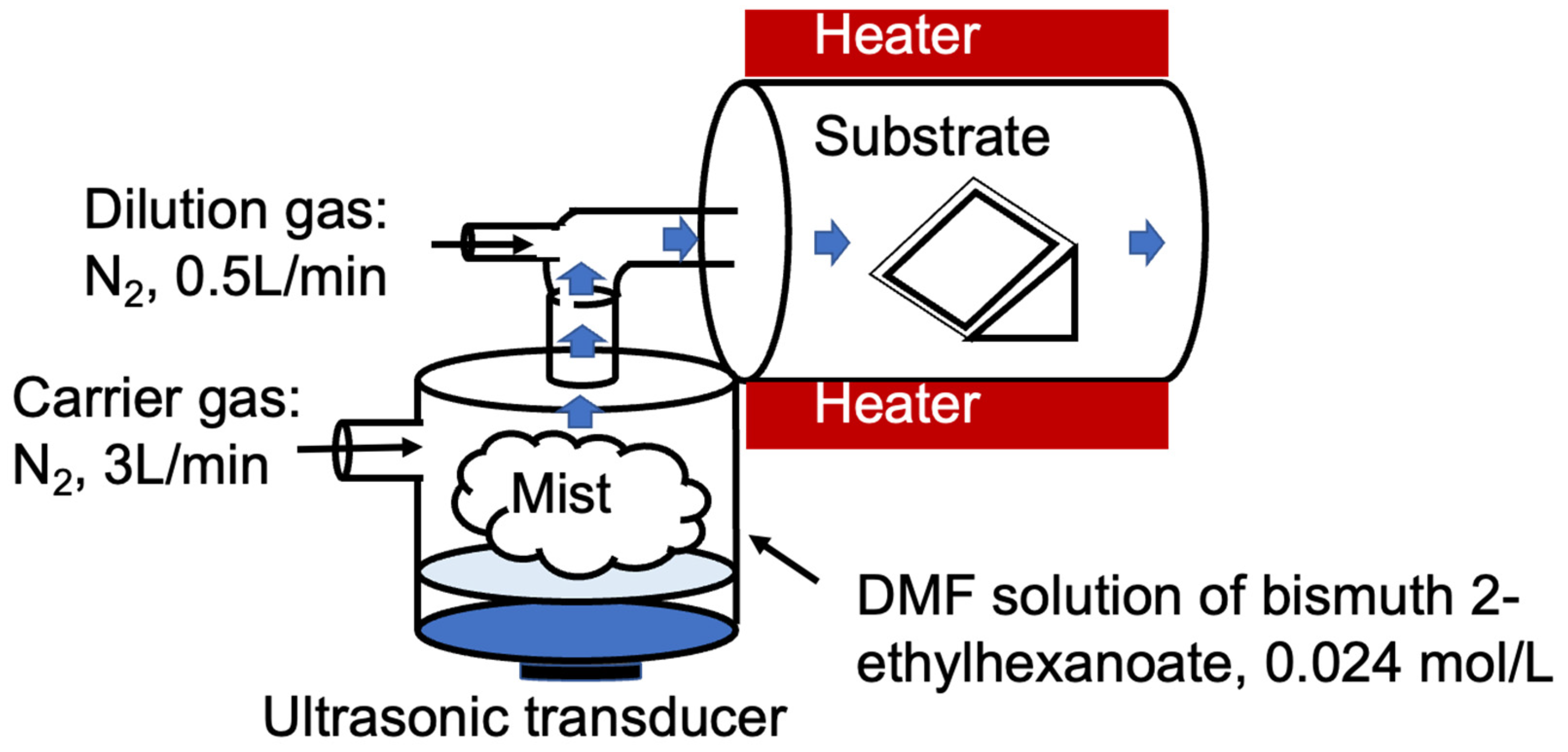
2.1. Thin Film Deposition

This study synthesized β-Bi2O3 thin films using mist CVD. The main chemical raw materials and equipment are shown in Table 2 and Figure 1.
In this study, β-Bi2O3 thin films were prepared on ITO (thickness 200 nm, resistance ≤ 6 Ω)-conductive glass substrates using the mist CVD method. To avoid the influence of water and oxygen in the air, the precursor materials were weighed in an inert environment glove box, and a 0.1 mol/L 25 wt% bismuth(III) 2-ethylhexanoate solution was prepared using DMF as the Bi source. The ITO glass was ultrasonically cleaned sequentially with acetone and ethanol for 15 min each in an ultrasonic cleaner to remove organic impurities from the substrate surface. After cleaning, the substrate was dried with nitrogen (N2) and set aside. The cleaned and dried ITO glass was then placed into a tube furnace and heated to a deposition temperature of 400 °C. Once the temperature of the tube furnace stabilized, nitrogen gas (N2) was introduced at a flow rate of 1 L/min for 15 min to provide an inert environment. Next, the precursor solution was poured into a nebulizing chamber and dispersed into droplets of approximately 5 µm using an ultrasonic device with a frequency of 2.4 MHz. Finally, driven by N2 at a flow rate of 3 L/min, it entered the tube furnace and was diluted with 0.5 L/min of N2. The reaction was maintained at a constant temperature for 15 min to obtain the β-Bi2O3 sample. After the reaction, the sample was cooled to room temperature under a nitrogen atmosphere before being taken out.

2.2. Characterization

The crystal structure and phase of the thin films were analyzed using X-ray diffraction (XRD) and Raman spectroscopy. The XRD instrument used was a Bruker D8 Discover (Bremen, Germany), with a copper target and a scanning angle range of 20–60°. The Raman spectrometer used was a Hitachi LamRam HR Evolution (Tokyo, Japan), with a laser wavelength of 532 nm and a test wavenumber range of 50–200 cm−1. Using an optical microscope (OM) to analyze the macroscopic surface morphology, the model is C3230BE (CG300) from Shanghai Precision Instrument Co., Ltd. (Shanghai, China). The transmittance and reflectance were measured using a UV-Vis-NIR spectrophotometer, specifically the Lambda 750 S from PerkinElmer. All electrochemical tests were conducted using a CHI660E electrochemical workstation from Chenhua Co., Ltd. (Shanghai, China). The prepared film, platinum electrode, and Ag/AgCl electrode served as the working electrode, counter electrode, and reference electrode, respectively. The effective test area of the working electrode was 1 cm2, with a distance of approximately 1 cm between the working and counter electrodes. KOH solution (0.5 mol L−1) saturated by N2 gas was used as the electrolyte according to the test requirements. LED lights with different wavelengths (365 nm, 455 nm, 520 nm, and 630 nm) and various power levels (ranging from 3 to 90 mW/cm2) were used as excitation light sources. The instantaneous current–time (i-t) curves were measured under a bias voltage ranging from 0 V to 0.6 V vs. RHE.

3. Results and Discussions

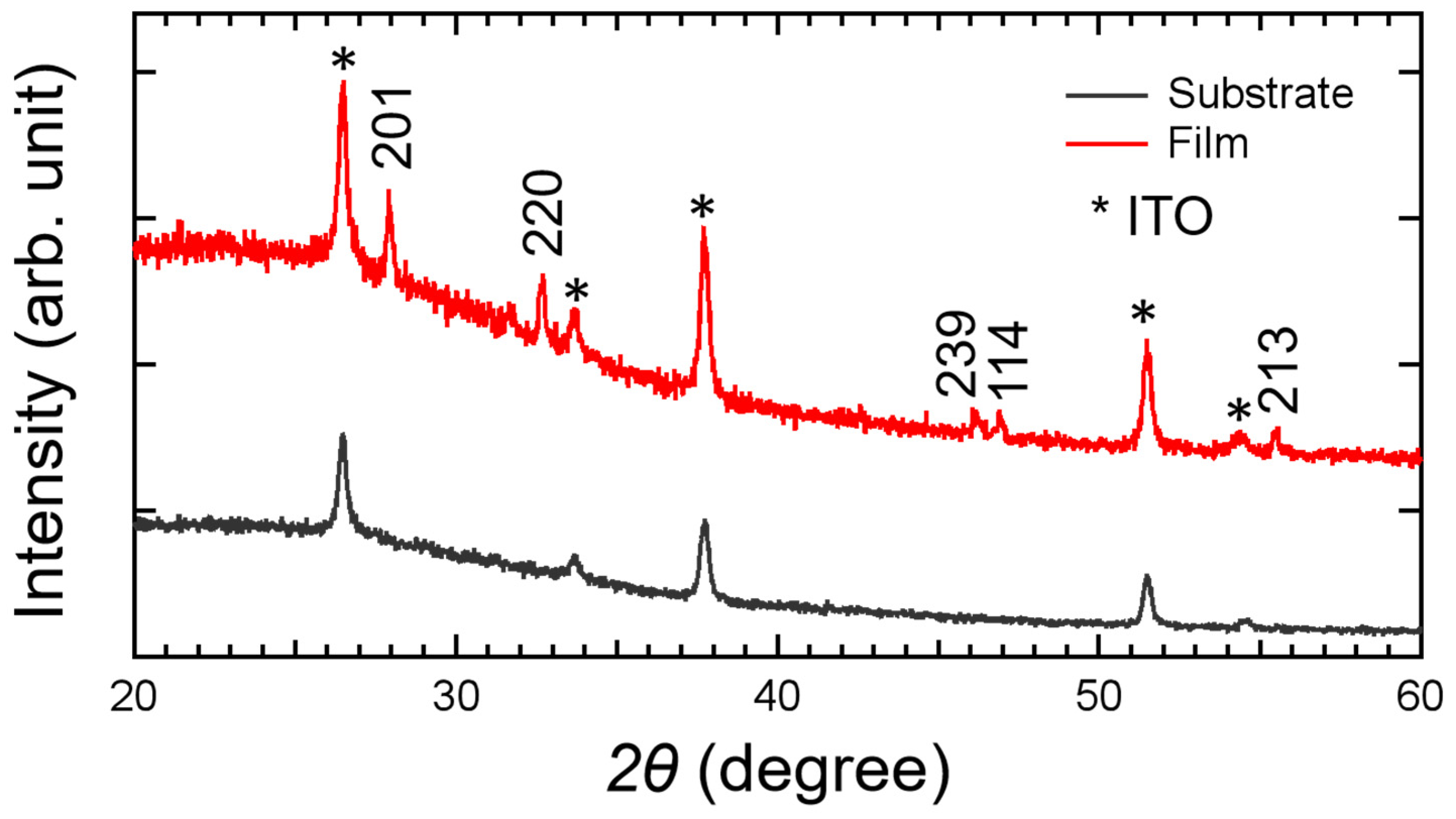
3.1. Phase Structure Analysis

To characterize the phase structure of the prepared samples, XRD testing was conducted on β-Bi2O3, and the results are shown in Figure 2. After comparing with the standard PDF card for β-Bi2O3 (01-077-5341), it can be observed that, aside from the diffraction peaks from the ITO glass substrate, the β-Bi2O3 sample shows diffraction peaks at 27.9°, 33.7°, 46.1°, 46.9°, and 55.5°, corresponding to the (201), (220), (239), (114), and (213) crystal planes of β-Bi2O3, respectively. No diffraction peaks of other substances were found, which fully indicates that the synthesized film is β-Bi2O3 with high purity. In addition, we calculated the lattice constant and grain size based on the Scherrer formula and Bragg equation, which was summarized in Table 3. The lattice constant is close to the theoretical values.
Usually, the β phase (201) peak (27.93°), α phase (012) peak (28.03°) (PDF: 01-070-8243), and δ phase (111) peak (27.95°) (PDF: 00-027-0052) have similar two values, so that it is not accurate to determine the crystal structure only based on the XRD θ-2θ patterns. In order to further confirm the crystal structure, the Raman spectra are necessary as these three phases have totally different Raman peaks. Figure 3 reveals from the Raman spectra of the β-Bi2O3 that all the peaks located at 119, 311 and 463 cm−1 in the pattern of the sample grown at 400 °C were well assigned to the β-Bi2O3 [24,25,26].

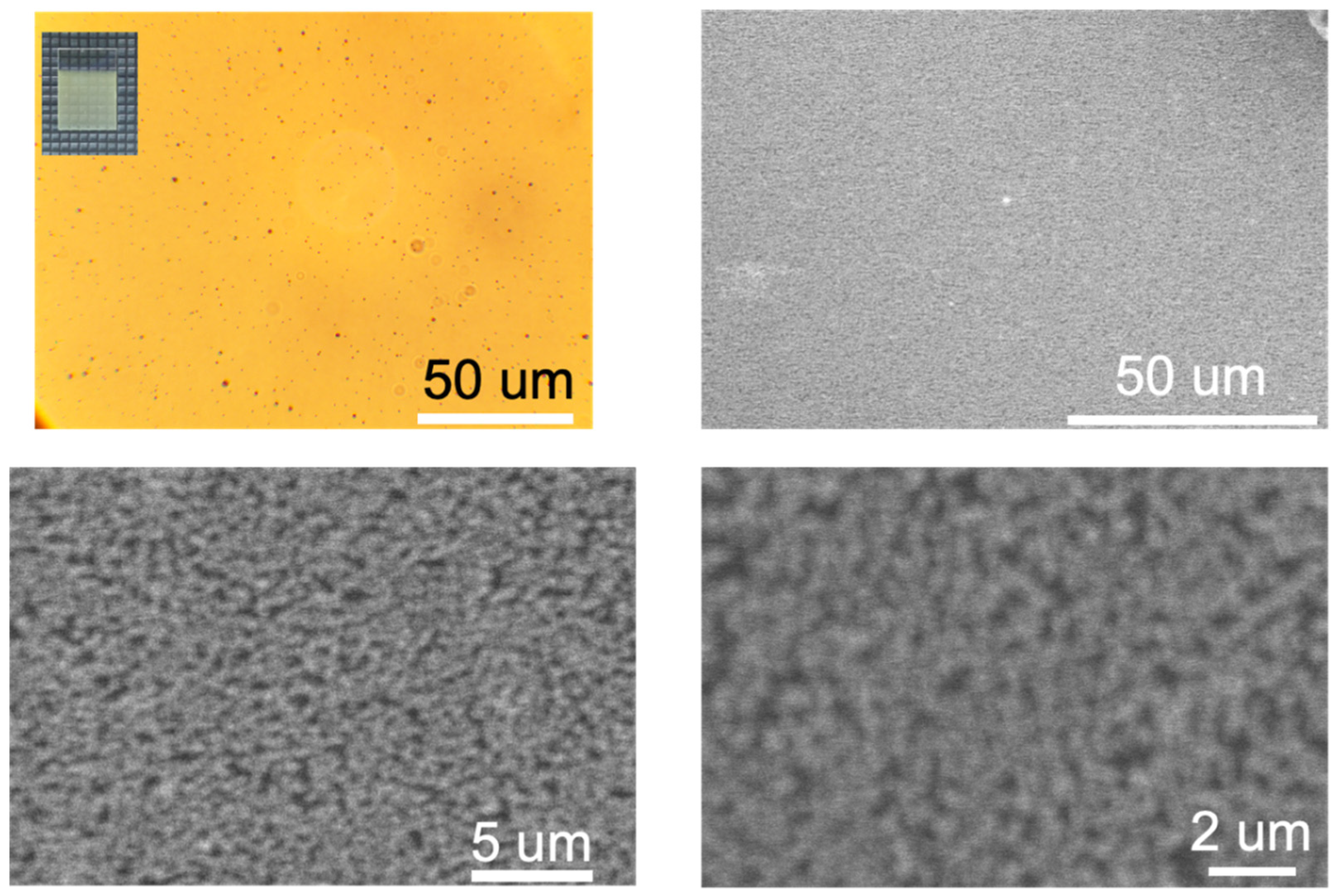
3.2. Surface Morphology

Figure 4 shows the photograph and microscopic morphology of the β-Bi2O3 film obtained at 400 °C. As seen in the figure, the β-Bi2O3 film obtained at 400 °C has a macroscopically continuous and uniform surface. The β-Bi2O3 film appears yellow. To further characterize the morphology of β-Bi2O3 films at different deposition temperatures, optical microscopy and SEM were used to observe the β-Bi2O3 films. The figure shows that the deposited β-Bi2O3 films are composed of aggregated particles, with a macroscopically continuous surface and a relatively uniform and dense film surface. The low resolution and/or inaccuracy might be caused by the amorphous impurities in the coating. In addition, we used EDS to detect the element composition of the β-Bi2O3 thin film (Figure 5). The molar ratio of Bi:O is 2:3.02, which is almost close to the theoretical value.

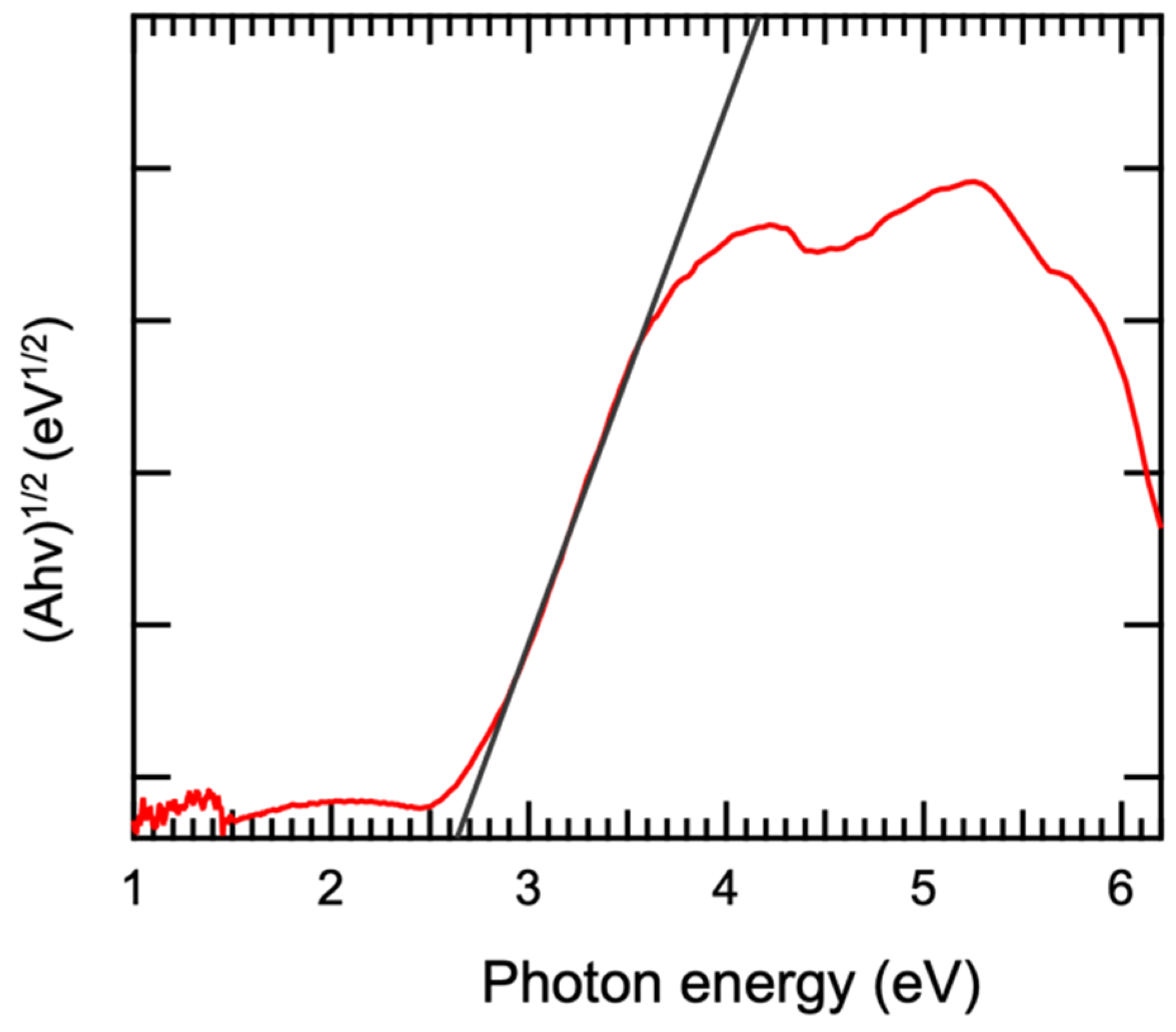
3.3. Optical Performance Analysis

Figure 6 shows the absorption spectrum of β-Bi2O3 thin film that β-Bi2O3 synthesized at 400 °C exhibits strong absorption of light below 400 nm wavelength, while weak absorption of high-wavelength light.
To further investigate the bandgap width of β-Bi2O3 thin films, the Tauc-plot method was used for estimation, and the calculation formula is as follows.
( α h v ) 1 n = B ( h v E g )
where α is the absorption coefficient, Planck’s constant h = 4.13566 × 10⁻¹⁵, B is a constant, v is the incident photon frequency, Eg is the bandgap, and n is determined by the type of semiconductor bandgap (for a direct bandgap semiconductor n = 1/2, and for an indirect bandgap semiconductor n = 2). Based on the calculation results and previous studies, the value of n is selected. After fitting the calculated graph, the tangent at the point with the maximum slope intersects the x-axis at the bandgap value. As shown in Figure 7, the bandgap of β-Bi2O3 is 2.6 eV.

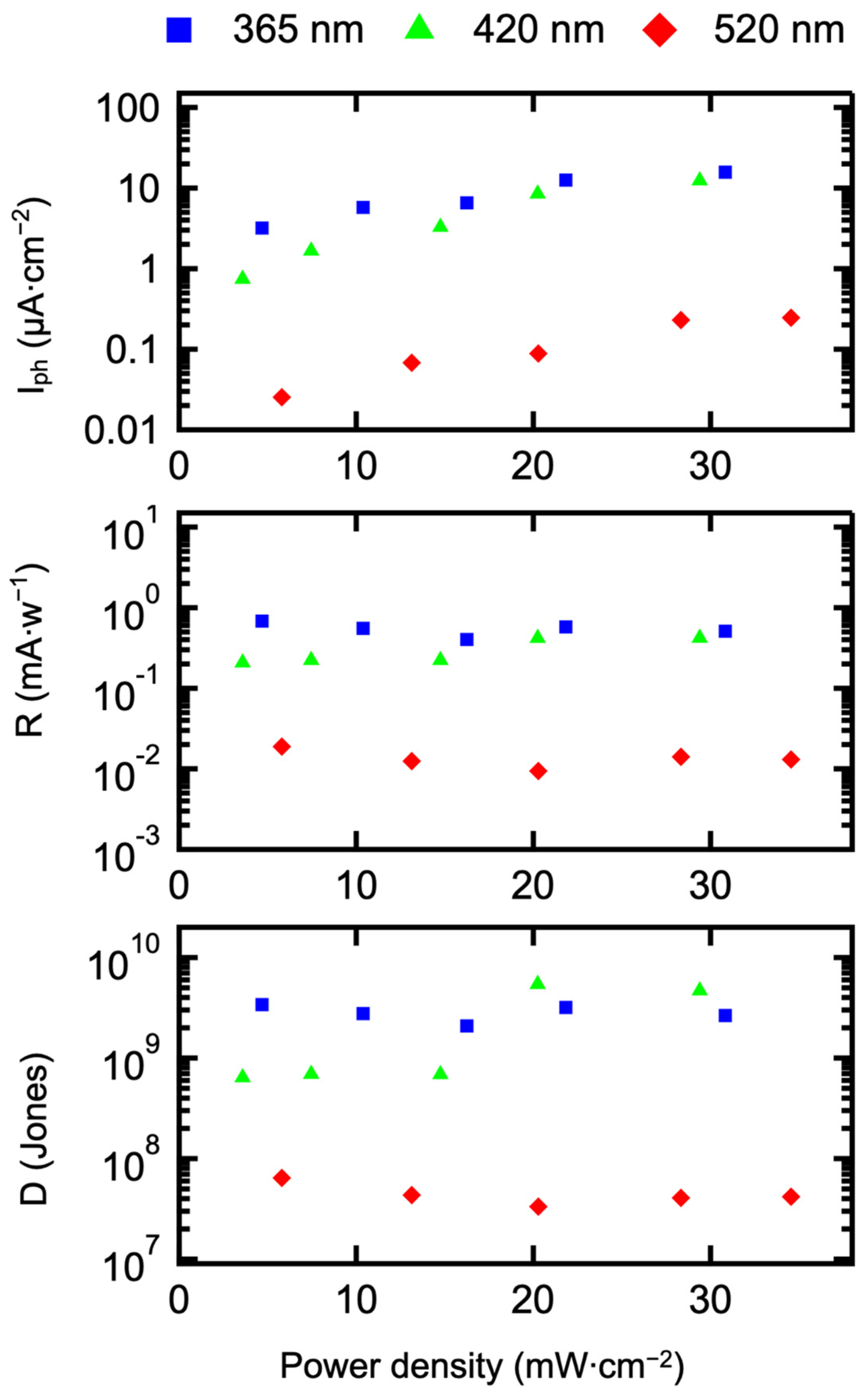
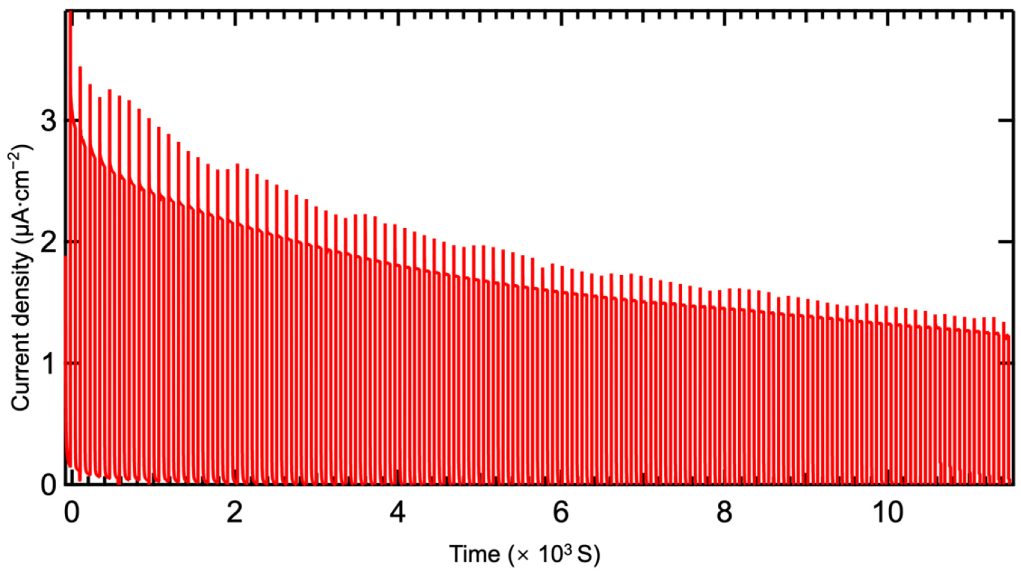
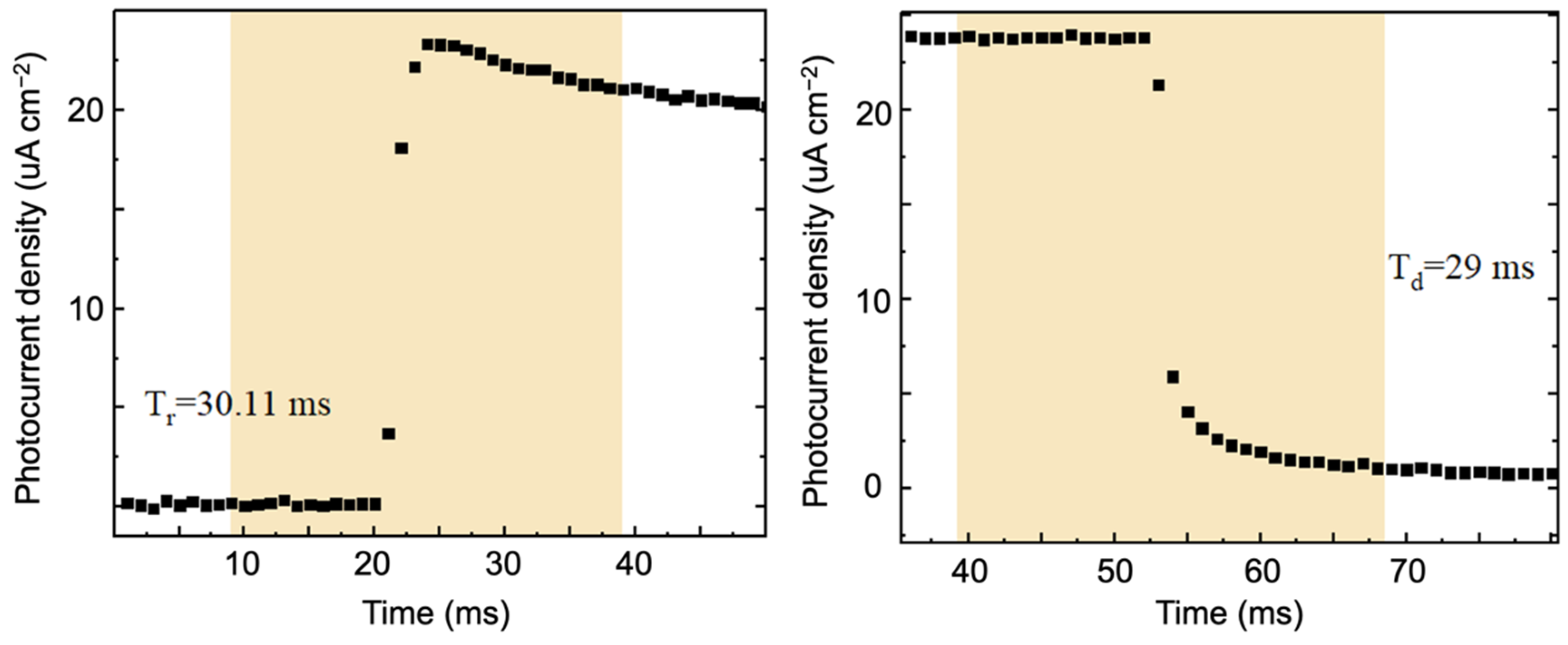
3.4. Construction and Performance Research of Photodetectors

In the photoelectrochemical-type photodetector, the β-Bi2O3 film obtained at 400 °C is used as the working electrode, with the platinum electrode and Ag/AgCl electrode serving as the counter electrode and reference electrode, respectively. The structure of the detector is shown in Figure 8. The electrolyte affects the transport process of charge carriers and can significantly impact the performance of the constructed photoelectrochemical device. In this study, 0.5 mol/L Na2SO4 was used as the electrolyte.
The detection capabilities of the β-Bi2O3-based photoelectrochemical photodetector for light sources with different wavelengths (365 nm, 420 nm, 520 nm) and powers were characterized, as shown in Table 4.
The variation of the photoresponse over time under illumination with light sources of different wavelengths and powers is shown in Figure 9. Under a bias of 0 V, the β-Bi2O3-based photoelectrochemical photodetector exhibits a significant photoelectric response to light sources ranging from 365 nm to 520 nm, indicating that the detector has self-powered characteristics and a wide detection range. At approximately low light source power density, the photocurrent value reaches around 3.3 µA∙cm−2 under illumination with a 365 nm light source. As the wavelength increases to 520 nm, the photocurrent value decreases to around 0.15 µA∙cm−2, which is related to its absorption characteristics. As the power density increases, the time-resolved curves gradually show instantaneous peaks, indicating the recombination of photogenerated charge carriers. When the recombination is more severe, the peak area is larger.
To characterize the current changes under illumination, the net photocurrent density (Iph) is introduced to measure the performance of the photodetector. The calculation formula of I p h is shown in Equation (2).
Iph = IlightIdark
where Ilight and Idark represent the photocurrent of the β-Bi2O3 photodetector under illumination and the dark current without illumination, respectively. Figure 10 shows the Iph of the β-Bi2O3 photodetector measured under different wavelengths and power densities. As shown in the figure, under illumination with a 365 nm light source, as the laser power density increases from 4.46 mW/cm2 to 21.64 mW/cm2, I p h increases from 3.2 μA/cm2 to 15.8 μA/cm2. This indicates that I p h gradually increases with increasing laser power density. This is attributed to the increased power, which increases the number of photons, causing more electrons in the valence band to transition to the conduction band, generating more photogenerated electron–hole pairs and transferring them, resulting in higher photocurrent density. Under similar laser power densities, as the light source wavelength increases from 365 nm to 520 nm, the I p h value decreases. This is consistent with the absorption characteristics of the β-Bi2O3 film at 400 °C, where light absorption gradually decreases with increasing wavelength.
The photodetection performance of the β-Bi2O3 photodetector at 400 °C depends on the wavelength and power of the incident light source. Responsivity (R) and detectivity (D*) can still be used to measure the performance of the photodetector, calculated as shown in Equations (3) and (4).
R = I p h / P
D * = R × S / 2 × q × I p h
The values of R and D* obtained from calculations based on I p h are also shown in Figure 10, where P represents the laser power density (mW/cm2), S is the effective light detection area (cm2), and q is the electronic charge (C). The relationship between R, D*, light power, and wavelength is derived from these calculations. Under a bias voltage of 0 V and constant wavelength of 365 nm, as the power density of the light source increases, the highest responsivity R reaches 0.68 mA/W, and the highest detectivity D* reaches 3.4 × 10⁹ Jones. Under illumination conditions with wavelengths of 365 nm, 420 nm, and 520 nm, the responsivity R values obtained are 0.68, 0.21, and 0.02 mA/W, respectively. The detectivity D* values obtained under illumination conditions with wavelengths of 365 nm, 420 nm, and 520 nm are 3.4 × 10⁹, 6.42 × 10⁸, and 6.45 × 10⁷ Jones, respectively. This indicates that under constant wavelength conditions, the detection capability of the β-Bi2O3 photodetector for photoelectrons decreases inversely with light power density. In other words, as the light power density increases, the detection capability of the β-Bi2O3 photodetector weakens. This phenomenon occurs because under high power density irradiation, the number of charge carriers in the β-Bi2O3 structure increases rapidly, leading to increased scattering between carriers, hindering their transfer and transport. This also increases the probability of electron–hole recombination, significantly increasing the recombination rate of carrier pairs per unit time. Furthermore, as the wavelength of light increases, photon energy decreases gradually, reducing the absorption capacity of the β-Bi2O3 film for light. Therefore, both the responsivity and detectivity of the β-Bi2O3 photodetector decrease accordingly.
In practical applications, long-term stability is a critical metric for evaluating the performance of photoelectrochemical photodetectors. To investigate the stability of the β-Bi2O3-based photoelectrochemical photodetector at 400 °C, this study utilized a 365 nm LED light source with a laser power density of 4.5 mW/cm2 and a cycling interval of 10 s for long-term i-t stability testing, as shown in Figure 11. After the first cycle, the photocurrent density was 2.8 μA/cm2. Following 500 on–off cycles, the photocurrent density decreased to 1.3 μA/cm2, indicating a decrease of approximately 1.5 μA/cm2. This demonstrates that after one hour of operation, the photodetector maintained approximately 45% of its initial photocurrent density, indicating acceptable on–off stability. After the PEC stability, we checked the surface morphology of β-Bi2O3 thin films that there were no clear changes observed (Figure 12).
Response time is primarily used to measure the speed at which a detector responds to incident light. It refers to the time it takes for the detector’s response output to rise to stability or fall back to the pre-irradiation value in response to a rectangular light pulse. A shorter response time indicates a faster detection speed for the detector. To investigate the response speed of the PEC photodetector based on the β-Bi2O3 to light, this study tested the response time at a wavelength of 365 nm and a power density of approximately 30 mW/cm2, with a testing step of 1 ms. The results, shown in Figure 13, depict the response time of the β-Bi2O3 photodetector. From the graph, it can be observed that the response speeds are τrise = 30.11 ms and τdecay = 29 ms, demonstrating an ultra-fast response speed compared to other materials, promising for achieving ultra-fast detection. Compared to bismuth-based semiconductor PEC-type photodetectors, the β-Bi2O3 PEC-type photodetector exhibited comparable and even superior photodetection performance in terms of responsivity, response time, and stability (Table 5).

4. Conclusions

In this paper, we synthesized the β-Bi2O3 thin films by the mist chemical vapor deposition method. The β-Bi2O3 film deposited at a temperature of 400 °C has high purity, a uniform and continuous surface, and a bandgap width of 1.35 eV. β-Bi2O3-based photoelectrochemical photodetectors have a wide light absorption range, self-driving properties, and high stability. The highest responsivity R and detection rate D* reached 2.84 mA/W and 6.01 × 10¹⁰ Jones, respectively. The response speeds of PEC photodetectors based on β-Bi2O3 at a wavelength of 365 nm and a power density of approximately 30 mW/cm2 are τrise = 30.11 ms and τdecay = 29 ms, respectively, showing an ultrafast response speed and promise for ultrafast detection. Additionally, carbon residue might occur during the deposition of Bi2O3 so post-annealing might be beneficial for the improvement in film quality. In addition, optimization of electrode architecture would be another strategy for the enhancement of PEC-type photodetection performance. Thus, this study would promote the practical applications of bismuth-based semiconductors.

Author Contributions

Software, J.Z.; Resources, Z.X.; Data curation, J.Z. and Z.W.; Writing—original draft, J.Z.; Writing—review & editing, Z.W. and J.S.; Visualization, Z.X.; Supervision, J.S.; Project administration, J.S.; Funding acquisition, J.Z., Z.X. and J.S. All authors have read and agreed to the published version of the manuscript.

Funding

This research was funded by Wuhan Key R&D Plan, grant number 2023020402010590, Scientific Research and Innovation Foundation of Sanya Yazhou Bay Science and Technology City, grant number HSPHDSRF-2023-03-001, Key R&D Project of Hainan Yourui Cohesion Technology Co., Ltd., grant number 20231201ZZKY002. We thank Fangqi Wu, Qinna Ren, Huiyu Chen and Weibojie Lu for their assistance in the data collection.

Institutional Review Board Statement

Not applicable.

Informed Consent Statement

Not applicable.

Data Availability Statement

All data generated or analyzed during the study are available from the corresponding author upon request. The data are not publicly available due to privacy.

Conflicts of Interest

Authors Jiaji Zhang and Zhihua Xiong were employed by the company Hainan Yourui Cohesion Technology Co., Ltd. The remaining authors declare that the research was conducted in the absence of any commercial or financial relationships that could be construed as a potential conflict of interest.

References

  1. Tang, R.; Zhou, S.; Zhang, Z.; Zheng, R.; Huang, J. Engineering nanostructure–interface of photoanode materials toward photoelectrochemical water oxidation. Adv. Mater. 2021, 33, 2005389. [Google Scholar] [CrossRef]
  2. Gopinath, C.S.; Nalajala, N. A scalable and thin film approach for solar hydrogen generation: A review on enhanced photocatalytic water splitting. J. Mater. Chem. A 2021, 9, 1353–1371. [Google Scholar] [CrossRef]
  3. Chen, Q.; Cheng, X.; Long, H.; Rao, Y. A short review on recent progress of Bi/semiconductor photocatalysts: The role of Bi metal. Chin. Chem. Lett. 2020, 31, 2583–2590. [Google Scholar] [CrossRef]
  4. Xu, M.; Yang, J.; Sun, C.; Liu, L.; Cui, Y.; Liang, B. Performance enhancement strategies of bi-based photocatalysts: A review on recent progress. Chem. Eng. J. 2020, 389, 124402. [Google Scholar] [CrossRef]
  5. Zahid, A.H.; Han, Q. A review on the preparation, microstructure, and photocatalytic performance of Bi2O3 in polymorphs. Nanoscale 2021, 13, 17687–17724. [Google Scholar] [CrossRef] [PubMed]
  6. Zhang, J.; Mei, B.; Chen, H.; Sun, Z. Review on synthetic approaches and PEC activity performance of bismuth binary and mixed-anion compounds for potential applications in marine engineering. Dalton Trans. 2024, 53, 10376–10402. [Google Scholar] [CrossRef]
  7. Utami, B.A.; Sutanto, H.; Hidayanto, E.; Alkian, I. Recent advances in doped, Bi2O3; its photocatalytic activity: A review. Int. J. Res. Rev. 2022, 9, 216–230. [Google Scholar] [CrossRef]
  8. Díaz-Guerra Viejo, C.; Almodóvar, P.; Camacho López, M.; Camacho López, S.; Piqueras de Noriega, J. Formation of beta-Bi2O3 and delta-Bi2O3 during laser irradiation of Bi films studied in-situ by spatially resolved Raman spectroscopy. J. Alloys Compd. 2017, 723, 520–526. [Google Scholar] [CrossRef]
  9. Kim, M.W.; Joshi, B.; Samuel, E.; Kim, K.; Kim, Y.I.; Kim, T.G.; Swihart, M.T.; Yoon, S.S. Highly nanotextured β-Bi2O3 pillars by electrostatic spray deposition as photoanodes for solar water splitting. J. Alloys Compd. 2018, 764, 881–889. [Google Scholar] [CrossRef]
  10. Li, Y.; Song, J.; Ji, Y.; Lu, X.; Tian, Q.; Chen, J.; Sui, Z. Bismuth/bismuth trioxide with a dual-carbon support for high and long life lithium storage. J. Phys. Chem. Solids 2022, 163, 110562. [Google Scholar] [CrossRef]
  11. Wu, Z.; Chong, M.C.; Zhang, S.; Li, J.; Zhu, Y. Regulating the crystal phase of bismuth-based semiconductors for promoted photocatalytic performance. Sci. China Chem. 2024, 67, 1839–1864. [Google Scholar] [CrossRef]
  12. Ilves, V.G.; Gaviko, V.S.; Murzakaev, A.M.; Sokovnin, S.Y.; Uimin, M.A.; Zuev, M.G. Phase transformation in air of Bi2O3 nanopowder produced by pulsed electron beam evaporation. Ceram. Int. 2023, 49, 21848–21854. [Google Scholar] [CrossRef]
  13. Guo, P.; Yin, F.; Zhang, J.; Chen, B.; Ni, Z.; Shi, L.; Han, M.; Wu, Z.; Li, G. Crystal-Phase and Surface-Structure Engineering of Bi2O3 for Enhanced Electrochemical N2 Fixation to NH3. ACS Appl. Mater. Interfaces 2024, 16, 17540–17552. [Google Scholar] [CrossRef] [PubMed]
  14. Falsetti, P.H.E.; Soares, F.C.; Rodrigues, G.N.; Del Duque, D.M.; de Oliveira, W.R.; Gianelli, B.F.; de Mendonca, V.R. Synthesis and photocatalytic performance of Bi2O3 thin films obtained in a homemade spin coater. Mater. Today Commun. 2021, 27, 102214. [Google Scholar] [CrossRef]
  15. Hofmann, M.; Rößner, L.; Armbrüster, M.; Mehring, M. Thin Coatings of α-and β-Bi2O3 by Ultrasonic Spray Coating of a Molecular Bismuth Oxido Cluster and their Application for Photocatalytic Water Purification Under Visible Light. ChemistryOpen 2020, 9, 277–284. [Google Scholar] [CrossRef] [PubMed]
  16. Cosham, S.D.; Hill, M.S.; Horley, G.A.; Johnson, A.L.; Jordan, L.; Molloy, K.C.; Stanton, D.C. Synthesis and materials chemistry of bismuth Tris-(di-i-propylcarbamate): Deposition of photoactive Bi2O3 thin films. Inorg. Chem. 2014, 53, 503–511. [Google Scholar] [CrossRef] [PubMed]
  17. Fernandez-Ibanez, P.; McMichael, S.; Cabanillas, A.R.; Alkharabsheh, S.; Moranchel, A.T.; Byrne, J.A. New trends on photoelectrocatalysis (PEC): Nanomaterials, wastewater treatment and hydrogen generation. Curr. Opin. Chem. Eng. 2021, 34, 100725. [Google Scholar] [CrossRef]
  18. Alulema-Pullupaxi, P.; Espinoza-Montero, P.J.; Sigcha-Pallo, C.; Vargas, R.; Fernández, L.; Peralta-Hernandez, J.M.; Paz, J.L. Fundamentals and applications of photoelectrocatalysis as an efficient process to remove pollutants from water: A review. Chemosphere 2021, 281, 130821. [Google Scholar] [CrossRef] [PubMed]
  19. Majumder, S.; Gu, M.; Kim, K.H. Effect of annealing of β-Bi2O3 over enhanced photoelectrochemical performance. Mater. Sci. Semicond. Process. 2022, 141, 106439. [Google Scholar] [CrossRef]
  20. Lu, Y.; Zhao, Y.; Zhao, J.; Song, Y.; Huang, Z.; Gao, F.; Li, N.; Li, Y. Induced aqueous synthesis of metastable β-Bi2O3 microcrystals for visible-light photocatalyst study. Cryst. Growth Des. 2015, 15, 1031–1042. [Google Scholar] [CrossRef]
  21. Selvamani, T.; Anandan, S.; Granone, L.; Bahnemann, D.W.; Ashokkumar, M. Phase-controlled synthesis of bismuth oxide polymorphs for photocatalytic applications. Mater. Chem. Front. 2018, 2, 1664–1673. [Google Scholar] [CrossRef]
  22. Schlesinger, M.; Schulze, S.; Hietschold, M.; Mehring, M. Metastable β-Bi2O3 nanoparticles with high photocatalytic activity from polynuclear bismuth oxido clusters. Dalton Trans. 2013, 42, 1047–1056. [Google Scholar] [CrossRef]
  23. Tang, X.; Ma, C.; Liu, N.; Liu, C.; Liu, S. Visible light β-Bi2O3/BiOCl heterojunction photocatalyst with highly enhanced photocatalytic activity. Chem. Phys. Lett. 2018, 709, 82–87. [Google Scholar] [CrossRef]
  24. Trentelman, K. A note on the characterization of bismuth black by Raman microspectroscopy. J. Raman Spectrosc. 2009, 40, 585–589. [Google Scholar] [CrossRef]
  25. Hardcastle, F.D.; Wachs, I.E. The molecular structure of bismuth oxide by Raman spectroscopy. J. Solid State Chem. 1992, 97, 319–331. [Google Scholar] [CrossRef]
  26. In, J.; Yoon, I.; Seo, K.; Park, J.; Choo, J.; Lee, Y.; Kim, B. Polymorph-Tuned synthesis of α-and β-Bi2O3 nanowires and determination of their growth direction from polarized raman single nanowire microscopy. Chem.–Eur. J. 2011, 17, 1304–1309. [Google Scholar] [CrossRef]
  27. Wang, K.; Qiao, H.; Li, J.; Qi, X. A robust photoelectrochemical photodetectors based on the self-healing properties of Bi2O2S nanoplates. Appl. Surf. Sci. 2021, 565, 150444. [Google Scholar] [CrossRef]
  28. Xu, L.; Yang, M.; Lu, Q.; Ren, Y.; Chen, Y.; Guo, J.; Cai, M.; Miao, X.; Teng, F.; Fan, H.; et al. 2D BiSeI Nanosheets for Broadband Self-Powered Photoelectrochemical Photodetector. Phys. Status Solidi (RRL)–Rapid Res. Lett. 2024, 18, 2300183. [Google Scholar] [CrossRef]
  29. Zhang, X.Y.; Wang, D.; Zeng, Z.; Zhao, C.; Liu, Y.; Zhang, B.; Pan, J.; Liu, D.; Wang, J. PVP-Assisted Hydrothermal Synthesis of Bi2O2Se Nanosheets for Self-Powered Photodetector. J. Sol. Energy Res. Updates 2022, 9, 1–8. [Google Scholar] [CrossRef]
  30. Zhang, H.; Luo, W.; Sun, Z.; Li, C. Highly Sensitive and Stable Visible-Light Self-Power Photodetectors Based on Solution-Processed Bi4O5I2. Cryst. Growth Des. 2023, 23, 2852–2859. [Google Scholar] [CrossRef]
  31. Yan, X.; Shi, B.; Cao, H.; Tian, Z.; Dai, C.; Liu, W.; Yang, Q.; Wang, Y. Flexible self-powered photoelectrochemical-type photodetectors based on Bi2O2S/GO composites. J. Mater. Chem. C 2023, 11, 6928–6934. [Google Scholar] [CrossRef]
  32. Zhao, G.; Sun, Z.; Mei, B. Oxygen Vacancies Modified Bi4O5I2 for Sensitive and Stable Photoelectrochemical-Type Photodetection. Adv. Opt. Mater. 2024, 12, 2302029. [Google Scholar] [CrossRef]
  33. Zhao, G.; Mei, B.; Chen, Y.; Sun, Z. Mist Chemical Vapor Deposition of Bi13S18I2 for Photoelectrochemical-type Photodetection. Inorg. Chem. 2024, 63, 3460–3466. [Google Scholar] [CrossRef] [PubMed]
Figure 1. Schematical image of mist CVD for β-Bi2O3 thin films.
Materials 17 03779 g001
Figure 2. XRD pattern of β-Bi2O3 thin film synthesized at 400 °C.
Materials 17 03779 g002
Figure 3. Raman spectra of β-Bi2O3 thin films synthesized at 400 °C.
Materials 17 03779 g003
Figure 4. Optical microscope and SEM image with various scale of β-Bi2O3 thin film synthesized at 400 °C.
Materials 17 03779 g004
Figure 5. EDS spectrum of β-Bi2O3 thin film synthesized at 400 °C.
Materials 17 03779 g005
Figure 6. Absorption spectrum of β-Bi2O3 thin film synthesized at 400 °C.
Materials 17 03779 g006
Figure 7. Tauc-plot of β-Bi2O3 thin film synthesized at 400 °C.
Materials 17 03779 g007
Figure 8. Structural diagram of β-Bi2O3 photodetector.
Materials 17 03779 g008
Figure 9. Time-resolved current graph of β-Bi2O3 photodetector illuminated by various wavelengths and power densities of illumination.
Materials 17 03779 g009
Figure 10. The Iph, R, and D of the β-Bi2O3 photodetector under different wavelengths and power density light irradiation.
Materials 17 03779 g010
Figure 11. Long-term stability for β-Bi2O3 synthesized at 400 °C with PEC-type photodetector.
Materials 17 03779 g011
Figure 12. SEM image of β-Bi2O3 thin film after the long-term stability test.
Materials 17 03779 g012
Figure 13. Response time graph of β-Bi2O3 photodetector.
Materials 17 03779 g013
Table 1. The summary of the preparation methods for β-Bi2O3 thin films.
MethodRef.TemperaturePrecursorTime
Solid-state reaction[14]450–600 °CBi2SiO52 h
Solution methods[15]300–500 °CBi38O45(OMc)24(DMSO)9·2DMSO·7H2O75 min
CVD[16]500–800 °CBismuth carbamate10–40 min
PVD[12]300–600 °CBi (001) film, BiOx, amorphous film30–35 min
Table 2. Experimental materials and manufacturers.
Chemical ReagentsChemical FormulaPurityManufacturer
25 wt% bismuth(III) 2-ethylhexanoate (C24H45BiO6)≥99.5%Aladdin (Shanghai, China)
N. N-DimethylformamideC3H7NO≥99.50%National Pharmaceutical Group (Beijing, China)
High purity nitrogen gasN2≥99.90%Wuhan Xiangyun Company (Wuhan, China)
Anhydrous ethanolC2H5OH≥99.00%National Pharmaceutical Group (Beijing, China)
Deionized waterH2O≥99.99%Self-prepared
AcetoneC3H6O≥99.00%National Pharmaceutical Group (Beijing, China)
Table 3. Crystal structure parameters calculated from the XRD pattern.
ParameterValue
a = b0.770 nm
c0.568 nm
Crystallite size18.90 nm
Table 4. Laser power density at different wavelength power percentages (mW/cm2).
WavelengthsIIIIIIIVV
365 nm4.466.5510.1215.3221.64
420 nm3.587.4514.7520.3429.40
520 nm5.7910.7613.1320.2828.33
Table 5. Photodetection performance of recently reported PEC-type photodetectors.
MaterialsRef.ElectrolyteLight
(nm)
Voltage
(V)
R
(mA/W)
τrd
(ms)
Stability
(per Cycle Decrease)
Bi2O2S[27]0.5 M KOHSun0.60.2380/70
BiSeI[28]0.2 M Na2SO46000.52.887/160.09%
Bi2O2Se[29]Na2SO3365014.249/12
Bi4O5I2[30]0.5 M Na2SO3420019.41.9/3.00.12%
Bi2O2S/GO[31]KOH/PVASun00.035420/23000.05%
OV-Bi4O5I2[32]0.5 M H2SO4365018.21.4/1.00.082%
Bi13S18I2[33]0.5 M Na2SO4 + 0.7M Na2SO3020.22.0/1.00.05%
β-Bi2O3This work0.5 M KOH36502.8430.1/29.10.09%
Disclaimer/Publisher’s Note: The statements, opinions and data contained in all publications are solely those of the individual author(s) and contributor(s) and not of MDPI and/or the editor(s). MDPI and/or the editor(s) disclaim responsibility for any injury to people or property resulting from any ideas, methods, instructions or products referred to in the content.

