Article

Micro/Nanomechanical Characterization of ScAlMgO4 Single Crystal by Instrumented Indentation and Scratch Methods

by
Zifeng Ni
1,2,*,
Jie Yu
1,
Guomei Chen
3,
Mingjie Ji
1,
Shanhua Qian
1,
Da Bian
1 and
Ming Liu
4,*
1
School of Mechanical Engineering, Jiangnan University, Wuxi 214122, China
2
Jiangsu Province Engineering Research Center of Micro-Nano Additive and Subtractive Manufacturing, Wuxi 214122, China
3
School of Electromechanical, Wuxi Vocational Institute of Commerce, Wuxi 214153, China
4
Fujian Provincial Key Laboratory of Terahertz Functional Devices and Intelligent Sensing, School of Mechanical Engineering and Automation, Fuzhou University, Fuzhou 350108, China
*
Authors to whom correspondence should be addressed.
Materials 2024, 17(15), 3811; https://doi.org/10.3390/ma17153811 (registering DOI)
Submission received: 3 June 2024 / Revised: 5 July 2024 / Accepted: 17 July 2024 / Published: 2 August 2024
(This article belongs to the Special Issue Advances of Indentation Technology in Materials)

Abstract

:
ScAlMgO4 (SCAM), which can be used as an epitaxial substrate material of GaN in power devices, faces the challenge of achieving a high-quality surface by ultra-precision polishing due to its brittle and easily cleaved characteristics, which are closely associated with its mechanical properties. The micromechanical properties of SCAM single crystals were evaluated by nanoindentation and microscratch tests using different indenters. The elastic modulus EIT and the indentation hardness HIT of SCAM obtained by nanoindentation were 226 GPa and 12.1 GPa, respectively. Leaf-shaped chips and the associated step-like planes of SCAM can be found in the severely damaged regime during scratching by Berkovich and Vickers indenters with sharp edges due to the intersection of intense radial and lateral cracks. The fracture toughness (Kc = 1.12 MPa·m1/2) of SCAM can be obtained by using a scratch-based methodology for a spherical indenter based on linear elastic fracture mechanics (LEFM) under an appropriate range of applied loads. An optimal expression for calculating the fracture toughness of easily cleaved materials, including SCAM, via the Vickers indenter-induced cracking method using a Berkovich indenter was recommended.

1. Introduction

The lattice match between a semiconductor material and the epitaxial substrate (e.g., sapphire [1] and SiC [2]) is key to achieving performance breakthroughs in power devices made of semiconductor materials (e.g., GaN single crystals of a wide forbidden bandwidth and a high insulating breakdown field strength) [3]. ScAlMgO4 (SCAM) is the most promising epitaxial substrate of semiconductor GaN due to the small lattice mismatch (i.e., 1.8%) between SCAM and GaN, which has close coefficients in thermal expansion along the a-axis (6.2 × 10⁻⁶/K for GaN and 5.6 × 10⁻⁶/K for SCAM) [4,5]. The substrate material should be prepared by ultra-precision polishing, during which the micro-scale removal of material is achieved, and thus the microscopic removal mechanism and micromechanical properties of the material have crucial impacts on ultra-precision polishing [6], which can be simulated by instrumented scratch with the indenter serving as a single abrasive particle against the crystal surface [7]. Scratch tests can also be used to characterize the tribological behavior [8], material properties [9], and surface damage [10] of different materials (e.g., ceramics [11], glasses [12], and metals [13]). Instrumented indentation has been widely used to characterize the mechanical properties, including the elastic modulus [14], indentation hardness [15], and fracture toughness [16], of different materials.
Ge et al. [17] performed scratch tests on the (001) plane of silicon single crystal using a Berkovich indenter and found that edge-forward and face-forward scratching resulted in different residual depths and material removal rates. Hou et al. [18] performed indentation tests on the (0001) plane of 4H-SiC single crystal wafer and established an analytical expression of the total energy dissipated during a single indentation cycle. Feng et al. [19] carried out scratch tests on the (0001) plane (i.e., C-plane) of sapphire and reported that scratch speed had significant effects on surface damage, chip formation, and penetration depth. Using Vickers, Knoop, and Berkovich indenters under various loads, Liu et al. [20] investigated the mechanical properties (e.g., elastic modulus, indentation hardness, and fracture toughness) of ZrO2 and Si3N4 by indentation and scratch methods and found that mechanical properties of material, indenter geometry, and loading conditions all greatly affected the obtained values of fracture toughness depending on scratch methodology.
The high-quality surface of ScAlMgO4 prepared by ultra-precision polishing is challenging due to its brittle and easily cleaved characteristics, which are closely associated with its mechanical properties (mainly hardness and fracture toughness [21,22]) and which are lacking in study. To provide some guidance for ultra-precision polishing, in this study, the mechanical properties of the machining surface of SCAM were examined by microscratch and nanoindentation tests with different indenters. Indentation hardness and elastic modulus under different loads were compared and discussed via the nanoindentation technique through the OP method with a Berkovich indenter. In addition, we focus on the characterization of fracture toughness, which plays a critical role in the brittle fracture of SCAM. The values of fracture toughness obtained by different methods, including microscratch approaches with a spherical indenter and the Vickers indenter-induced cracking method with a Berkovich indenter, were compared and discussed.

2. Materials and Experimental Methods

2.1. SCAM Wafer

SCAM has a crystal structure of YbFe2O4 and consists of a hexagonal crystal system with the R 3 ¯ m spatial group, with each crystal cell containing three SCAM molecules, as shown in Figure 1. Sc3+ occupies the position of Yb in the YbFe2O4 crystal structure, forming an octahedral structure with six O2− ions, and Al3+/Mg2+ randomly occupies the position of Fe in the YbFe2O4 crystal structure, forming an [Al/MgO5] triangular bipyramid structure of five O2− ions [23]. SCAM is considered a type of (RAO3)n(MO)m group oxide (n = m = 1 for SCAM; R3+ indicates rare-earth metallic elements such as In/Lu/Y/SC; A3+ can consist of metallic elements such as Fe/Ga/Al; and M2+ can consist of metallic elements such as Mg/Co/Cu/Zn) [24]. SCAM tends to cleave along the (0001) plane, making it challenging to obtain a high-quality wafer surface. Two types of Al/Mg-O bonds will result in two different (0001) planes, as represented by [Al/Mg-O]1 and [Al/Mg-O]2, respectively. SCAM can cleave at [Al/Mg-O]1, mainly due to weak interconnections between the layer of [ScO6] and [Al/MgO5] by O2- irons [25]. SCAM can also cleave at [Al/Mg-O]2, mainly due to the reverse symmetry that can cancel the electric dipole moment and surface charges [26].
Figure 2 shows the X-ray photoelectron spectroscopy (XPS, EscaLab 250Xi, Thermo Fisher, Waltham, MA, USA) of the SCAM wafer with the following dimensions: 10 × 10 × 0.5 mm3 (Goetsu Semiconductor WuXi Co., Ltd., Wuxi, China) before polishing. The fine spectra of Sc 2p, Mg 2s, Al 2p, and O 1s of SCAM are also shown as insets. The Sc 2p of SCAM corresponds to the Sc-O bond with two different binding energies of 402.5 eV and 406.9 eV, respectively [27]. Mg 2s and Al 2p correspond to Mg-O (binding energy of 1305.5 eV) and Al-O (binding energy of 74.4 eV) bonds, respectively [28,29]. The peaks of O 1s at 530.6 eV and 531.8 eV correspond to the Sc-O-Sc and Sc-OH bonds (due to water in air), respectively [30].
Colloidal SiO2 particles about 100 nm in size (Wujiang Chuangyuan New Material Technology Co., Ltd., Suzhou, China) were used as the polishing slurry. Potassium hydroxide KOH (Sinopharm Chemical Reagent Co., Ltd., Beijing, China) was selected as a pH regulator. SCAM wafers were polished under a pH of 8, an abrasive particle concentration of 20 wt.%, and a slurry flow rate of 200 mL/min on JY-M15P (Jeng Yueh Enterprise Co., Ltd., New Taipei City, Taiwan) to ensure the surface quality for subsequent nanoindentation and microscratch tests. The polished wafers were ultrasonically cleaned with anhydrous ethanol and deionized water, and the surfaces were blow-dried using an air gun.
Figure 3a shows the metallographic microscope image of the SCAM surface after polishing with a down pressure of 0.5 kg/cm2 and a platen speed of 80 r/min. Cleavages appear as colored waves due to the large down pressure of 0.5 kg/cm2 applied for polishing. Figure 3b shows the effects of the polishing down pressure (under a fixed platen speed of 80 r/min) and a platen speed (under a fixed polishing down pressure of 0.2 kg/cm2) on the roughness average Ra measured by atomic force microscopy (scan area of 10 × 10 μm2). The down pressure and platen speed should be optimized to obtain the lowest Ra. A sharp increase in Ra occurs as the down pressure increases to 0.5 kg/cm2, which is the reason for the formation of cleavages shown in Figure 3a. The down pressure has a greater influence on Ra than platen speed. The optimal polishing conditions for the lowest Ra can be determined to be a down pressure of 0.2~0.3 kg/cm2 and a platen speed of 60~80 r/min.
Figure 4a,b compare the scanning electron microscopy (SEM) images of the SCAM surfaces before and after polishing under a platen speed of 80 r/min and a down pressure of 0.2 kg/cm2. Step-like cleavage planes, cleavage pits, and local smooth areas exposed by cleavages can be observed on the initial surface of the easily cleaved SCAM, as shown in Figure 4a. The rough surface of the SCAM wafer becomes smooth and without cleavages after polishing under optimized conditions, and the polished surfaces are suitable for subsequent nanoindentation and microscratch tests.

2.2. Microscratch of SCAM

Instrument scratch tests were performed on an MST2 (Anton Paar, Graz, Austria) microscratch tester equipped with acoustic emission (AE) [31], and three different types of indenters were used, namely a diamond Berkovich indenter with a face angle of 65.27° (resulting in the same ratio of the projected contact area over the contact depth as the Vickers indenter) [32], a diamond Vickers indenter, and a spherical indenter made of steel (i.e., 100Cr6) with a radius of 500 μm. Tests were conducted on the plane that had a deviation of 16°12′ degrees from the (0001) plane (i.e., the 10 × 10 mm2 surface of the wafer) of SCAM with a scratch direction parallel to one side of the 10 × 10 mm2 surface. The scratch distance was 3 mm, and the thrust was in the edge-forward direction for the sharp indenters. The normal load Fv was progressively increased from the initial 5 mN to three different maximum loads (i.e., 0.5 N, 5 N, and 25 N) within 30 s in the scratch tests with a spherical indenter at a scratch speed of 6 mm/min. Four different scratch speeds (i.e., 3, 6, 12, and 18 mm/min) were applied in the microscratch tests using Berkovich and Vickers indenters, and the normal load Fv was progressively increased from the initial 5 mN to a maximum of 500 mN. Since the scratch speed was much lower than the processing speeds during grinding and polishing, the thermal effect was negligible. The scratch test consisted of four steps [33]: (1) the initial surface profile or sample tilt of the SCAM wafer was measured during the pre-scan phase under a small vertical load of 5 mN, whose effect on plastic deformation was negligible [34]; (2) scratching under the prescribed conditions; (3) post-scan under a small vertical load of 5 mN, and the residual depth could be obtained; and (4) capture of scratch morphology by optical microscopy [35]. The residual scratch morphologies obtained by optical microscopy were synchronized with the variations of scratch variables, such as penetration depth dp representing total deformation, residual depth dr representing plastic deformation, friction coefficient μ (i.e., the ratio of lateral force over normal load), and acoustic emission (AE) during scratching as Fv increased [36]. The horizontally projected contact area Ah and the vertically projected contact area Av for different indenters are illustrated in Figure 5 and [37]:
A h = { 3 d p 2 tan α   for   Berkovich   indenter ,   and   α = 65.27 ° 2 d p 2 tan ψ   for   Vickers   indenter ,   and   ψ = 68 ° R 2 arccos R d p R ( R d p ) R 2 ( R d p ) 2   for   spherical   indenter
A v = { 2 3 d p 2 tan α   f ο r   Berkovich   indenter ,   and   α = 65.27 ° 2 d p 2 tan ψ   for   Vickers   indenter ,   and   ψ = 68 °

2.3. Nanoindentation of SCAM

Instrumented indentation tests of SCAM were performed on a NHT2 (Anton Parr) nanoindentation tester by a Berkovich indenter with a face angle of 65.27° under both the loading and unloading times of 30 s, a holding time of 10 s, and a sampling frequency of 10 Hz. Indentation tests were conducted on the same surface and in the same direction as the scratch tests. Both loading and unloading segments of the indentation load-displacement curve can be fitted by simple power law functions as follows [38]:
F = { k 1 h n 1   for   loading F max ( h h p h max h p ) m   for   unloading
where k1 and n1 are fitting parameters; F and h are indentation load and displacement, respectively, with the subscript “max” indicating the maximum value; m is an exponent ranging between 1.2 and 1.7 for most materials [39,40]; and hp is the permanent indentation displacement (i.e., the residual indentation displacement after unloading).
The reduced plane strain modulus Er of the contact area is a combination of the plane strain modulus of the sample and that of the indenter and can be obtained from the contact stiffness S [41] (i.e., the initial slope of the unloading curve at hmax):
E r = 1 ( 1 ν 2 E IT + 1 ν i 2 E i ) = π S 2 β 1 A p ( h c ) ,   S = d P d h | h max
where EIT and ν denote the elastic modulus and Poisson’s ratio (ν = 0.2 is used for SCAM) of the sample, respectively; and Ei = 1141 GPa and νi = 0.07 are the elastic modulus and Poisson’s ratio of the diamond indenter, respectively. β1 = 1.034 is the correction factor for a Berkovich indenter lacking axial symmetry [41].
Both indentation hardness HIT, which is the mean projected contact pressure, and contact depth hc can be obtained at hmax:
H I T = F max A p ( h c ) , h c = h max ε F max S
where Ap is the projected contact area at hmax. Since the calibration of indenters is the basis for obtaining accurate mechanical properties of tested materials via the OP method [42], the Ap(hc) of the Berkovich indenter was calibrated by performing nanoindentation tests on a standard fused silica with known elastic modulus of 73 GPa and a Poisson’s ratio of 0.17 under various loads (≤100 mN for fused silica in order to avoid cracking) with B-spline interpolation in ambient laboratory condition, and ε depends on the value of m [43].

3. Results and Discussion

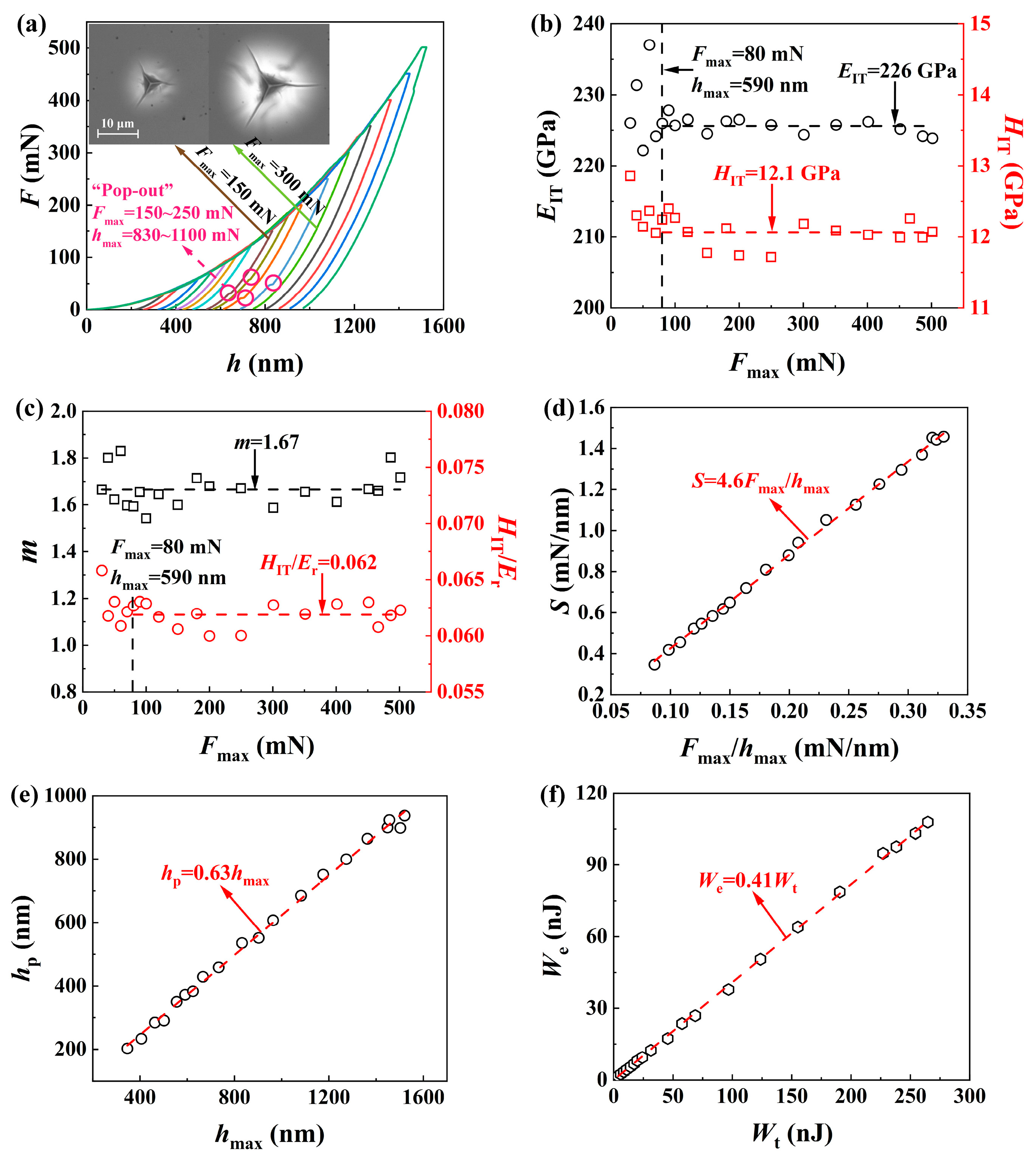
3.1. Analysis of Nanoindentation of SCAM by a Berkovich Indenter

Figure 6a shows the load-displacement (F-h) curves of SCAM under different loads of Fmax for SCAM, and the creep effect during the holding period is negligibly small for brittle solids. The elastic recovery during the unloading indicated that both elastic deformation and plastic deformation played significant roles during the indentation of hard and brittle SCAM at the nanoscale. When Fmax = 150 mN, radial cracks and the “pop-out” phenomenon (i.e., a reverse small jump in the penetration depth during unloading) were observed, which could be attributed to the cleavage fracture of SCAM. The “pop-out” phenomenon was sensitive to the applied load and disappeared under large loads (i.e., Fmax > 300 mN) when complex cracking systems were generated on the subsurface region, under which conditions cleavage fractures played a less significant role in indentation-induced damage.
Figure 6b shows variations of nanoindentation hardness HIT and elastic modulus EIT with Fmax. The decrease in HIT and EIT with increasing Fmax under small loads (i.e., Fmax < 80 mN) could be attributed to residual stresses after polishing. Both HIT and EIT reached constant levels (i.e., HIT = 12.1 GPa, EIT = 226 GPa) when Fmax ≥ 80 mN, indicating that HIT and EIT of SCAM were insensitive to indentation-induced damage (i.e., cleavage fracture and radial cracks).
Figure 6c shows variations of m and HIT/Er with Fmax. A constant m of 1.67 could be approximated for SCAM. HIT/Er tended to decrease as the load increased under small loads (i.e., Fmax < 80 mN), which could be attributed to elastic deformation and surface effect. A constant HIT/Er of 0.062 was calculated for SCAM under large loads and was smaller than those of brittle glass (i.e., HIT/Er = 0.10 for K9 glass [40] and HIT/Er = 0.13 for fused silica [41]), demonstrating that SCAM is less brittle than glass.
Figure 6d shows the proportional relationship between the contact stiffness S and Fmax/hmax, which could be used to continuously measure S with the load and displacement measured during the loading segment without the need of unloading, resulting in determining both HIT and EIT under different loads (or penetration depths) from only one loading test [44].
Figure 6e shows that the permanent depth hp is also proportional to the maximum indentation displacement hmax. hp/hmax = 0.63 for SCAM is smaller than 0.7, indicating the absence of pile-up [45], which was confirmed by the insets in Figure 6a. hp/hmax = 0.63 for SCAM is larger than those of fused silica (i.e., 0.48) [41] and K9 glass (i.e., 0.55) [40], which also indicates SCAM is less brittle than glass.
Figure 6f shows that elastic deformation work We, which can be calculated by integrating the unloading load-displacement curve, is proportional to the total mechanical work Wt of the indentation, which can be calculated by integrating both the loading and holding segments of the load-displacement curve. We/Wt was about 41% for SCAM due to the prominent roles of both elastic deformation and plastic deformation during nanoindentation of brittle material. We/Wt of SCAM was smaller than those of fused silica (i.e., 0.65) [41] and K9 glass (i.e., 0.55) [40], which also indicates SCAM is less brittle than glass.
The residual indentation morphologies of SCAM at four different loads are shown in Figure 7a–d. Only micro-cleavages were found on the wafer surface under small loads, see Figure 7a for Fmax = 30 mN. Obvious cleavages were observed at the edges of the residual imprint under relatively large loads, see Figure 7b for Fmax = 100 mN. Radial cracks initiated from the three vertices of residual imprints by the Berkovich indenter under sufficiently large loads, see Figure 7c for Fmax = 250 mN. As Fmax continued to increase, radial cracks and cleavages expanded, see Figure 7d for Fmax = 400 mN.

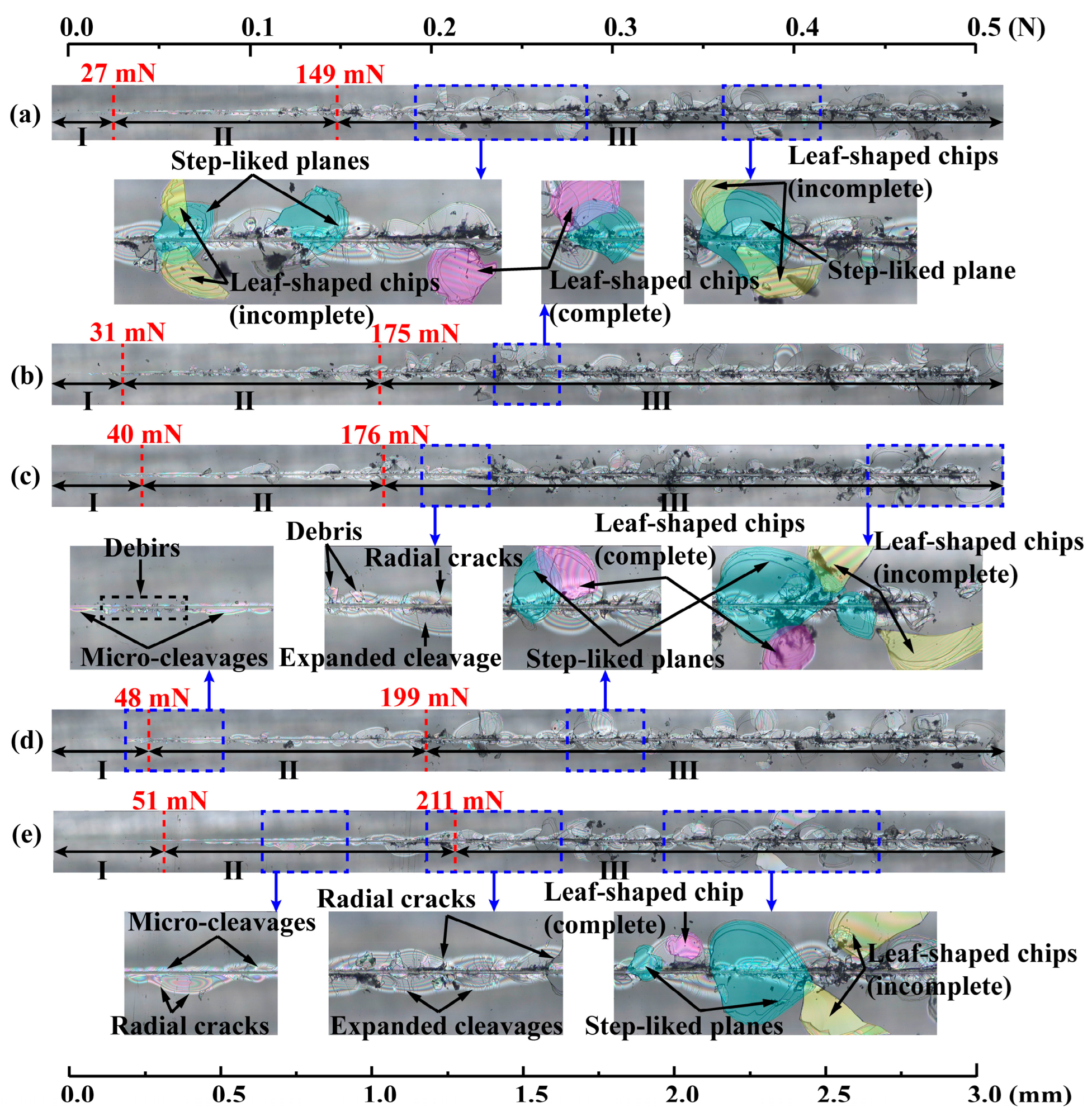
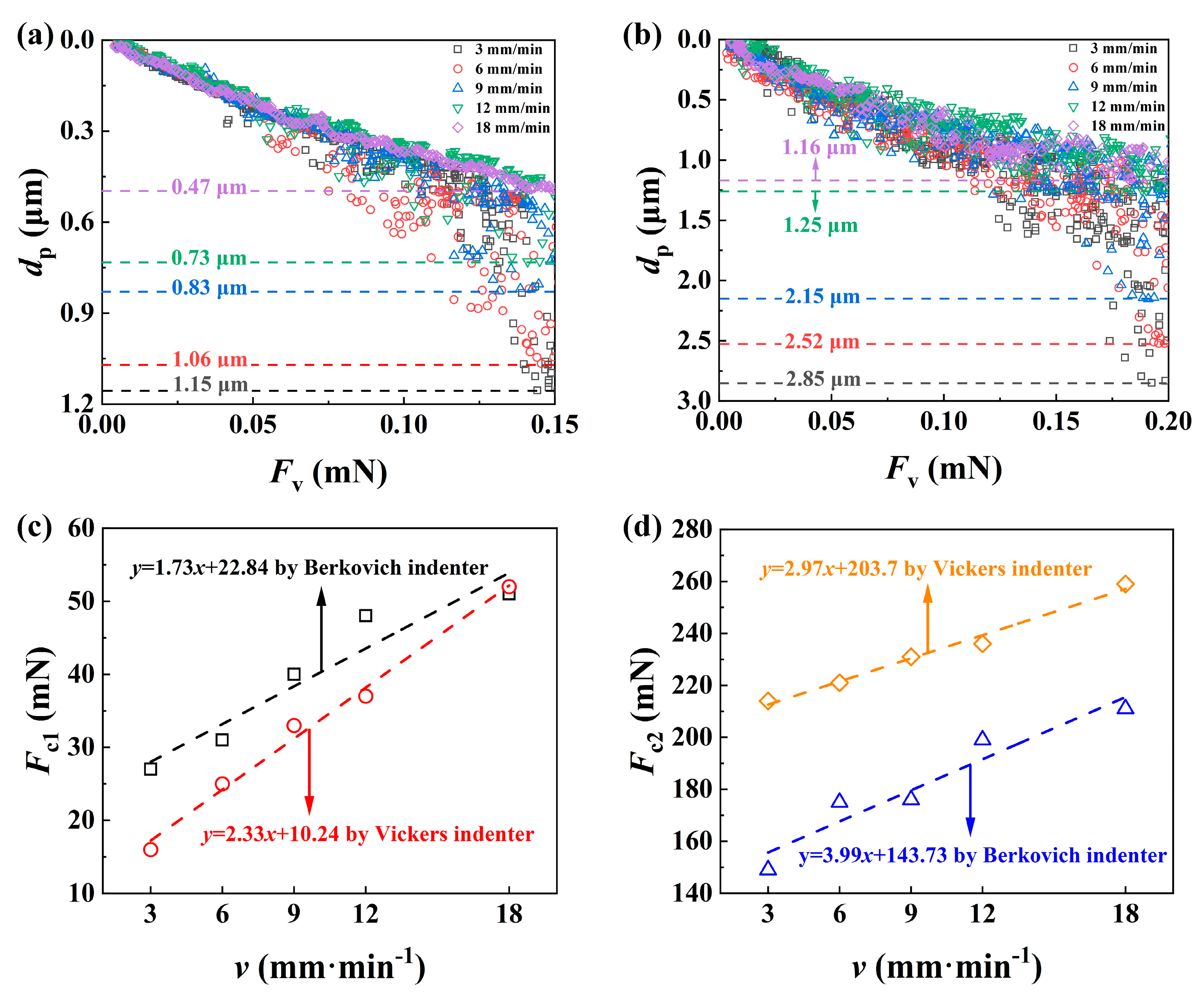
3.2. Analysis of Microscratch of SCAM by Different Indenters

Figure 8a–e show the variations of scratch variables including dp, residual depth dr, friction coefficient μ, and acoustic emission (AE) with the applied normal load Fv by a Berkovich indenter under progressive load that linearly increased from 5 mN to 500 mN and with different scratch speeds (i.e., 3, 6, 9, 12, and 18 mm/min). Figure 9a–e show the corresponding residual scratch morphologies that were synchronized with the scratch variables. Three different regimes were identified based on the variations of the scratch variables. In regime I under small loads, AE remained at low levels; friction coefficient μ vibrated around a low level; dp increased in an approximately linear and smooth way with increasing Fv; dr was negligible; and micro-cleavages were seen in the absence of cracking. The transition from regime I to regime II was denoted by the clearly increasing trends of μ and AE. In regime II under intermediate loads, both AE and μ increased with the increase in Fv; vibrations in dr and dp became prominent; the continuous appearance of micro-cleavages with their expansion was seen; debris, as well as lateral and radial cracks, appeared in the absence of leaf-shaped chips. The transition from regime II to regime III was denoted by the abrupt change in dr and dp, together with the sharp increase in AE. In regime III under large loads, the increasing trend of μ gradually slowed down and vibrated around 0.37; significant fluctuations in dp, dr, and AE occurred; lateral and radial cracks intensively and continuously appeared; the step-like planes marked by blue color were generated by the peeling off of leaf-shaped chips marked in purple in Figure 9; and the expanded cleavages of a ripple shape similar to the cleavages by polishing as shown in Figure 3a were clearly seen. Both complete and incomplete leaf-shaped chips were seen and marked by purple and yellow colors, respectively, in Figure 9: one step-like plane was associated with two incomplete leaf-shaped chips or one complete leaf-shaped chip. The range in regime I was very small compared with those of regimes II and III, indicating the brittle characteristics of SCAM.
Figure 10a–e show the variations of scratch variables with the applied load Fv by a Vickers indenter under a linearly increasing load from 5 mN to 500 mN and different scratch speeds (i.e., 3, 6, 9, 12, and 18 mm/min). Three different regimes were identified based on the variations of scratch variables, which were synchronized with the residual groove morphologies as shown in Figure 11a–e. In regime I under small loads, μ vibrated significantly; AE intensity remained at a low level; dr was almost zero; and dp increased with increasing Fv in an approximately linear way; debris was seen, while micro-cleavages or radial cracks were hardly observed. The transition from regime I to regime II was denoted by the stabilization of μ and a clearly increasing trend of both AE and dr. In regime II under intermediate loads, μ stabilized at around 0.3; AE kept increasing with no abrupt change; both dr and dp increased with Fv in an almost linear way; and micro-cleavages, radial and lateral cracks, leaf-shaped chips, and step-like planes were observed. The transition from regime II to regime III was denoted by the abrupt increase in AE, which was associated with the large fluctuation of dr spanning from zero to the value that deviated far from the linear trend. The debris accumulated in the scratch groove had a significant effect on dr, resulting its fluctuation and value of almost zero [40]. In regime III under large loads, μ vibrated within a smaller range of around 0.3; significant fluctuations in dr, dp and AE occurred due to severe damage; continuously and intensively expanded cleavages, large radial and lateral cracks, leaf-shaped chips, step-like planes, and a large amount of debris was seen. With a Vickers indenter, μ vibrated significantly under small loads, and stabilized at about 0.3 under intermediate loads, while μ with a Berkovich indenter vibrated, kept increasing under intermediate loads, and reached a constant level of about 0.37 under large loads. The increase in μ was partly attributed to the interaction between leaf-shaped chips and indenter, and a larger μ was associated with more leaf-shaped chips [46]. Under large loads, leaf-shaped chips were destroyed and turned into debris [47], resulting in a constant level of μ. Although Berkovich (face angle of 65.27°) and Vickers (face angle of 68°) indenters can be regarded to be equivalent for indentation, a Vickers indenter can cause more serious damage compared to a Berkovich indenter, since the two sharp edges of a Vickers indenter that are perpendicular to the scratch direction can exert more squeeze on the sample. Three of the four sharp edges of a Vickers indenter play significant roles in scratching, while two of the three sharp edges of a Berkovich indenter cannot play an effective cutting role as one thrusts the material in front of the indenter. Therefore, a considerable amount of leaf-shaped chips can be turned into debris under smaller loads by a Vickers indenter, resulting in an earlier entry of μ into a stable level compared with a Berkovich indenter.
The generation mechanism of leaf-shaped chips and the corresponding step-like planes by a sharp indenter (e.g., Berkovich and Vickers indenters) is shown in Figure 12. Radial cracks, which occur together with the expanded cleavages, can intersect with lateral cracks that extend upwards to the surface of the sample under large loads [7], forming leaf-shaped areas to be delaminated (i.e., generation of leaf-shaped chips) due to the easily cleaved characteristics of SCAM. When the sharp indenter scratched through the leaf-shaped area in front of the indenter, the leaf-shaped chip was divided into two halves. When the leaf-shaped area was generated on the side of the scratch, and was peeled off from the sample, a complete leaf-shaped chip was generated. The step-like planes were exposed fresh surfaces after peeling off of the leaf-shaped chips.
In addition, according to the adhesion-ploughing friction theory, the friction force between two contact surfaces can be split into two parts: adhesion friction and ploughing friction [48]. Accordingly, the experimentally measured scratch friction coefficient μ can be divided into the adhesion friction coefficient μa and the ploughing friction coefficient μp:
μ = μ a + μ p , μ pB = A h B A v B , μ pV = A h V A v V , μ a = μ μ p
where the subscripts “B” and “V” indicate Berkovich and Vickers indenters, respectively; μpB and μpV are ploughing friction coefficients for Berkovich and Vickers indenters, respectively, and can be computed with Equations (1) and (2). A value of μpV = 0.29 is almost the same as a value of μ = 0.3 for a Vickers indenter under large loads, indicating the predominant role of brittle fractures with severe damage and negligible plasticity of the material. A value of μpB = 0.23 is much smaller than a value of μ = 0.37 for a Berkovich indenter under large loads, which can be explained by noting that two of the three sharp edges of the Berkovich indenter are more capable of generating pile-up than causing damage.
Figure 13a,b compare the penetration depth dp of SCAM under different scratch speeds using the Berkovich indenter under the maximum applied Fv = 150 mN and using the Vickers indenter under the maximum applied Fv = 200 mN, respectively, since the data of dp become very scattered under large loads due to severe damage. A higher v tends to produce a smaller dp, which has been widely reported in the literature, and increasing the scratch speed can reduce the penetration ability of the indenter [49,50], resulting in a greater applied load for the same penetration effect under a lower scratch speed. Figure 13c,d show the effects of scratch speed on the two critical loads Fc1 and Fc2, respectively, and both Fc1 and Fc2 increased in an approximately linear way as the scratch speed increased for both indenters, since a larger v resulted in a smaller dp and thus less damage, which corroborates the fact that increasing the platen speed within a certain range during polishing can reduce Ra of the material, see Figure 3b.
Figure 14a–c show the variations of scratch variables with the applied vertical load Fv during scratching by a spherical intender under three progressive loads (i.e., 5~500 mN, 5 mN~5 N, and 5 mN~25 N). dp increased with increasing Fv in an approximately linear way, which has been widely reported in the literature for different materials (i.e., ceramic, copper, and glasses) [47,51,52], and the proportional coefficient of dp against Fv decreased as the range of Fv increased due to the more prominent increase in contact area. AE intensity stabilized at about 3.4%, and values of dr were negligibly small, indicating the absence of severe damage by the blunt spherical indenter. Although μ could be constant under small loads, it tended to increase slowly as Fv increased, and a prominent increasing trend of μ was seen under large loads. This trend could be attributed to subsurface cracking, under which the fracture toughness was calculated based on the scratch methodology.

3.3. Characterization of Fracture Toughness by Microscratch Method

Fracture toughness Kc of a brittle solid was calculated by the scratch-based methodology based on linear elastic fracture mechanics (LEFM) for axisymmetric indenters [52,53]:
σ h = F h A h = K c Λ , Λ = A h 2 l p
where σh is the nominal strength, Λ is the nominal size, Ah and lp are the horizontally projected load-bearing contact area and the perimeter of the fracture surface, respectively, as shown in Figure 5a for a spherical intender. And lp was calculated for a spherical indenter:
l p = 2 R arccos R d p R
Figure 15a–c show the variation of σN with Λ obtained by a spherical indenter with a radius of 500 μm under different progressive loads of 5~500 mN, 5 mN~5 N, and 5 mN~25 N. Kc was obtained by curve fitting σN vs. Λ using Equation (3), when σN decreases with increasing Λ. Figure 15a shows that Kc obtained under Λ < 0.25 μm was 0.44 MPa·m1/2, which was smaller than the reasonable values since cracking was not developed under small loads by a blunt indenter, under which the predominate role of elastic-plastic deformation resulted in an almost constant level of scratch friction coefficient as shown in Figure 14a. Figure 15b shows that Kc obtained under 0.25 μm < Λ < 1.8 μm was about 1.1 MPa·m1/2, which was a reasonable value since the semi-circular horizontal crack plane in front of the indenter assumed in LEFM was well developed, which was demonstrated by the increase in scratch friction coefficient as shown in Figure 14b. Figure 15c shows that a σN vs. Λ curve could not be fitted well under a large Λ, and σN even tended to increase, which could be explained by noting the formation of complex cracking and surface damage under large loads, which made the assumption of a cracking plane in LEFM invalid. An appropriate fitting curve under a suitable range of a normal load was used for the characterization of fracture toughness by a scratch-based method in order to avoid either a crack-free or a severe damage situation.

3.4. Characterization of Fracture Toughness by Indenter-Induced Cracking

Fracture toughness of materials was also obtained by the indenter-induced cracking technique based on Griffith-Irwin equilibrium fracture mechanics, whose applicability is still under debate, since different materials exhibit different cracking systems (e.g., radial, median, and transverse cracks) under different loads. The semi-empirical expressions proposed for a Vickers indenter are listed in Table 1, and were multiplied by the correction factor kB = f(4)/f(3) = 1.073 when applied to a Berkovich indenter [54], since values of fracture toughness measured by Vickers and Berkovich indenters are linearly dependent:
f ( n ) = n / 2 1 + n 2 π sin 2 π n
where n is the number of radial cracks (n = 4 for a Vickers indenter; and n = 3 for a Berkovich indenter), and HV was replaced by HB, which was calculated as the ratio of the applied load F over the actual imprint area AB:
H B = F A B = 4 3 9 F sin α a 2 0.7 F a 2 ,   α = 65.27 °
Fracture toughness was obtained from the slope of the proportional fitting of the characteristic variables listed in Table 2, as shown in Figure 16. Radial cracks were invisible on the material surface under small loads (i.e., Fmax ≤ 120 mN), and only data under large loads (i.e., Fmax > 120 mN) were used for analysis. The Kc values calculated by the thirteen expressions listed in Table 1 are listed in Table 2, and only P-1, M-5, and C-2 gave reasonable values of Kc close to those obtained by the LEFM-based scratch method (i.e., 1.12 MPa·m1/2).
In general, low-toughness materials exhibit Palmqvist cracking, while medium cracking is found in materials with high toughness values. Actually, both types of cracking can be encountered in most materials [68], and a formal criterion based on the ratio c/a has been proposed to determine the type of cracking (i.e., Palmqvist cracking occurs when c/a < 2.5 and median cracking appears when c/a ≥ 2.5). The definitions of c, a, and l with the units of µm are shown in Figure 7d for the Berkovich indenter. It is understandable that almost all of the equations proposed for Palmqvist cracking underestimate the Kc value of SCAM under median cracking since c/a > 2.5 when Fmax > 120 mN. Interestingly, C-2, which provides a reasonable Kc value of SCAM, has also provided a reasonable Kc value of an NaCl single crystal with a (100) cleavage plane [69] in previous research [66]. It is noteworthy that C-2 and M-5 have almost the same form, while M-5 has a more physical background than C-2, and the use of C-2 is not recommended due to the ambiguous exponent (i.e., −1.56) of (c/a). In brief, although P-1, M-5, and C-2 can give reasonable values of Kc, only M-5 is recommended for SCAM, and it can be used as an optimal expression for calculating Kc values of other brittle and easily cleaved crystals.

4. Conclusions

Due to the easily cleaved nature of SCAM single crystals along its c-axis, it was challenging to obtain a high-quality surface via grinding and polishing, and the micromechanical properties of SCAM played a significant role in its ultra-precision polishing. Instrumented indentation with a Berkovich indenter and microscratch tests by spherical, Berkovich, and Vickers indenters were carried out on SCAM to study the deformation and damage under contact loading. As the load in nanoindentation increased, the damage became more and more severe, and micro-cleavages, cleavages, and radial cracks were observed. Elastic modulus and indentation hardness of SCAM obtained by nanoindentation were insensitive to indentation-induced damage under large, applied loads and were regarded as constant (i.e., EIT = 226 GPa and HIT = 12.1 GPa). Three different regimes were identified during scratching by Berkovich and Vickers indenters based on the morphologies of residual grooves, which were closely related to the variations and sudden changes of the scratch variables, including penetration depth, residual depth, friction coefficient, and acoustic emission. As the normal load increased during the scratch test, the damage became more and more severe, and debris, cracks, cleavages, leaf-shaped chips, and the associated step-like planes were found on the material’s surface. The blunt spherical indenter did not cause severe damage to the material under the loads applied in this study. Fracture toughness Kc = 1.12 MPa·m1/2 was obtained via scratch methodology with a spherical indenter based on linear elastic fracture mechanics. Fracture toughness was also obtained via the Vickers indenter-induced cracking technique using a Berkovich indenter, and an optimal expression was recommended for SCAM and other brittle and easily cleaved materials.

Author Contributions

Z.N.: conceptualization, funding acquisition, resources, methodology, writing—original draft; J.Y.: conceptualization, methodology, data curation, writing—original draft; G.C.: funding acquisition, resources; M.J.: conceptualization, methodology, data curation; S.Q.: funding acquisition, resources; D.B.: funding acquisition, resources; M.L.: conceptualization, methodology, data curation, resources, supervision, writing—review & editing. All authors have read and agreed to the published version of the manuscript.

Funding

S. Qian acknowledges the financial support provided by the National Natural Science Foundation of China (Grant Nos. 52375184). D. Bian acknowledges the financial support provided by the National Natural Science Foundation of China (Grant Nos. 52205169). M Liu acknowledges the financial support provided by the National Natural Science Foundation of China (Grant No. 51705082).

Institutional Review Board Statement

Not applicable.

Informed Consent Statement

Not applicable.

Data Availability Statement

The data presented in this study are available on request from the corresponding author. (due to privacy).

Conflicts of Interest

The authors declare that they have no known competing financial interests or personal relationships that could have appeared to influence the work reported in this paper.

References

  1. Shin, J.; Noh, S.; Lee, J.; Kim, J.S.; Choi, I.; Ahn, H.-K. Structural and electrical characteristics of ultra-thin Si-doped GaN film regrown on patterned GaN/sapphire. J. Korean Phys. Soc. 2023, 82, 963–969. [Google Scholar] [CrossRef]
  2. Yang, Q.; Li, Z.; Peng, D.; Li, C.; Zhang, D.; Xu, X. Growth of high quality GaN on (0001) 4H-SiC with an ultrathin AlN nucleation layer. J. Cryst. Growth 2023, 607, 127107. [Google Scholar] [CrossRef]
  3. Meneghini, M.; De Santi, C.; Abid, I.; Buffolo, M.; Cioni, M.; Khadar, R.A.; Nela, L.; Zagni, N.; Chini, A.; Medjdoub, F. GaN-based power devices: Physics, reliability, and perspectives. J. Appl. Phys. 2021, 130, 181101. [Google Scholar] [CrossRef]
  4. Chaoyi, Z.; Huili, T.; Xianke, L.; Qingguo, W.; Ping, L.; Feng, W.; Chenbo, Z.; Yanyan, X.; Jun, X.; Jianfeng, H.; et al. Research Progress of ScAlMgO4 Crystal: A Novel GaN and ZnO Substrate. J. Inorg. Mater. 2023, 38, 228–242. [Google Scholar]
  5. Ohnishi, K.; Kuboya, S.; Tanikawa, T.; Iwabuchi, T.; Yamamura, K.; Hasuike, N.; Harima, H.; Fukuda, T.; Matsuoka, T. Reuse of ScAlMgO4 substrates utilized for halide vapor phase epitaxy of GaN. Jpn. J. Appl. Phys. 2019, 58, SC1023. [Google Scholar] [CrossRef]
  6. Wang, W.; Yao, P.; Wang, J.; Huang, C.; Kuriyagawa, T.; Zhu, H.; Zou, B.; Liu, H. Elastic stress field model and micro-crack evolution for isotropic brittle materials during single grit scratching. Ceram. Int. 2017, 43, 10726–10736. [Google Scholar] [CrossRef]
  7. Huang, W.; Yan, J. Deformation behaviour of soft-brittle polycrystalline materials determined by nanoscratching with a sharp indenter. Precis. Eng. 2021, 72, 717–729. [Google Scholar] [CrossRef]
  8. Santos, M.D.; Fukumasu, N.K.; Tschiptschin, A.P.; Lima, N.B.d.; Figueroa, C.A.; Weber, J.S.; Souza, R.M.d.; Machado, I.F. Effect of Ti/Si and Ti/TiN/Si interlayers on the structure, properties, and tribological behavior of an a-C film deposited onto a C17200 copper-beryllium alloy. Surf. Coat. Technol. 2022, 441, 128561. [Google Scholar] [CrossRef]
  9. Liu, M.; Hou, D.; Zheng, K.; Gao, C. Characterization of friction and wear of phenolic resin matrix composites reinforced by bamboo fibers of alkaline and LaCl3 treatment. Mater. Today Commun. 2023, 35, 106361. [Google Scholar] [CrossRef]
  10. Davis, C.S.; Rencheck, M.L.; Woodcock, J.W.; Beams, R.; Wang, M.; Stranick, S.; Forster, A.M.; Gilman, J.W. Activation of mechanophores in a thermoset matrix by instrumented scratch. ACS Appl. Mater. Interfaces 2021, 13, 55498–55506. [Google Scholar] [CrossRef]
  11. Duan, W.; Yang, Z.; Cai, D.; Zhang, J.; Niu, B.; Jia, D.; Zhou, Y. Effect of sintering temperature on microstructure and mechanical properties of boron nitride whisker reinforced fused silica composites. Ceram. Int. 2020, 46, 5132–5140. [Google Scholar] [CrossRef]
  12. Liu, H.; Zhang, J.; Zhao, M.; Lu, C. Determination of the fracture toughness of glasses via scratch tests with a vickers indenter. Acta Mech. Solida Sin. 2022, 35, 129–138. [Google Scholar] [CrossRef]
  13. Fu, H.; Cai, L.; Chai, Z.; Liu, X.; Zhang, L.; Geng, S.; Zhang, K.; Liao, H.; Wu, X.; Wang, X. Evaluation of bonding properties by flat indentation method for an EBW joint of RAFM steel for fusion application. Nucl. Mater. Energy 2020, 25, 100861. [Google Scholar] [CrossRef]
  14. Raturi, A.; Biswas, K.; Gurao, N. Elastic and plastic anisotropy in a refractory high entropy alloy utilizing combinatorial instrumented indentation and electron backscatter diffraction. J. Alloys Compd. 2022, 896, 162902. [Google Scholar] [CrossRef]
  15. Peng, G.; Liu, Y.; Xu, F.; Jiang, H.; Jiang, W.; Zhang, T. On determination of elastic modulus and indentation hardness by instrumented spherical indentation: Influence of surface roughness and correction method. Mater. Res. Express 2023, 10, 086503. [Google Scholar] [CrossRef]
  16. Yu, F.; Fang, J.; Omacht, D.; Sun, M.; Li, Y. A new instrumented spherical indentation test methodology to determine fracture toughness of high strength steels. Theor. Appl. Fract. Mech. 2023, 124, 103744. [Google Scholar] [CrossRef]
  17. Ge, M.; Zhu, H.; Ge, P.; Zhang, C. Investigation on residual scratch depth and material removal rate of scratching machining single crystal silicon with Berkovich indenter. Mater. Sci. Semicond. Process. 2019, 100, 98–105. [Google Scholar] [CrossRef]
  18. Hou, D.; Liu, M.; Liu, S.; Yang, F. Indentation fracture of 4H-SiC single crystal. Int. J. Mech. Sci. 2024, 270, 109096. [Google Scholar] [CrossRef]
  19. Feng, P.-F.; Zhang, C.-L.; Wu, Z.-J.; Zhang, J.-F. Effect of scratch velocity on deformation features of C-plane Sapphire during nanoscratching. Stroj. Vestn. J. Mech. Eng. 2013, 59, 367–374. [Google Scholar] [CrossRef]
  20. Liu, M.; Chen, S. Micromechanical characterization of zirconia and silicon nitride ceramics using indentation and scratch methods. Ceram. Int. 2024, 50, 19982–20010. [Google Scholar] [CrossRef]
  21. Ness, E.; Zibbell, R. Abrasion and erosion of hard materials related to wear in the abrasive waterjet. Wear 1996, 196, 120–125. [Google Scholar] [CrossRef]
  22. Hai, K.; Li, L.; Hu, H.; Zhang, Z.; Bai, Y.; Luo, X.; Yi, L.; Yang, X.; Xue, D.; Zhang, X. Distribution model of the surface roughness in magnetorheological jet polishing. Appl. Opt. 2020, 59, 8740–8750. [Google Scholar] [CrossRef]
  23. Grajczyk, R.; Subramanian, M. Structure-property relationships of YbFe2O4- and Yb2Fe3O7-type layered oxides: A bird’s eye view. Prog. Solid State Chem. 2015, 43, 37–46. [Google Scholar] [CrossRef]
  24. Kimizuka, N.; Mohri, T.; Nakamura, M. Compounds which have InFeO3(ZnO)m-type structures (m = integer). J. Solid State Chem. 1989, 81, 70–77. [Google Scholar] [CrossRef]
  25. Katase, T.; Nomura, K.; Ohta, H.; Yanagi, H.; Kamiya, T.; Hirano, M.; Hosono, H. Large domain growth of GaN epitaxial films on lattice-matched buffer layer ScAlMgO4. Mater. Sci. Eng. B 2009, 161, 66–70. [Google Scholar] [CrossRef]
  26. Hanada, T.; Tajiri, H.; Sakata, O.; Fukuda, T.; Matsuoka, T. Characterization of the ScAlMgO4 cleaving layer by X-ray crystal truncation rod scattering. J. Appl. Phys. 2018, 123, 205305. [Google Scholar] [CrossRef]
  27. Haseman, M.S.; Noesges, B.A.; Shields, S.; Cetnar, J.S.; Reed, A.N.; Al-Atabi, H.A.; Edgar, J.H.; Brillson, L.J. Cathodoluminescence and x-ray photoelectron spectroscopy of ScN: Dopant, defects, and band structure. APL Mater. 2020, 8, 081103. [Google Scholar] [CrossRef]
  28. Seyama, H.; Soma, M. X-ray photoelectron spectroscopic study of montmorillonite containing exchangeable divalent cations. J. Chem. Soc. Faraday Trans. 1 Phys. Chem. Condens. Phases 1984, 80, 237–248. [Google Scholar] [CrossRef]
  29. Bou, M.; Martin, J.; Le Mogne, T.; Vovelle, L. Chemistry of the interface between aluminium and polyethyleneterephthalate by XPS. Appl. Surf. Sci. 1991, 47, 149–161. [Google Scholar] [CrossRef]
  30. Grosso, D.; Sermon, P. Scandia optical coatings for application at 351 nm. Thin Solid Film. 2000, 368, 116–124. [Google Scholar] [CrossRef]
  31. Liu, M.; Xu, Z. Scratch responses of ductile materials by instrumented scratch with a spherical indenter under progressive load. Sci. Sin. Phys. Mech. Astron. 2023, 53, 244612. [Google Scholar] [CrossRef]
  32. Liu, M.; Wang, W. Effects of sliding velocity on microscratch responses of thermoplastics by Berkovich indenter. Polym. Bull. 2023, 80, 7901–7926. [Google Scholar] [CrossRef]
  33. Liu, M.; Xu, Z.; Zhang, G. Effects of Dopants on Scratch Responses of Diamond-Like Carbon Films by Rockwell C Diamond Indenter. J. Mater. Eng. Perform. 2023, 32, 6092–6106. [Google Scholar] [CrossRef]
  34. Gao, C.; Liu, M. Effect of sample tilt on measurement of friction coefficient by constant-load scratch testing of copper with a spherical indenter. J. Test. Eval. 2020, 48, 970–989. [Google Scholar] [CrossRef]
  35. Liu, M.; Xie, P. Rate and Load Effects on Scratch Behavior of Thermoplastics by Berkovich Indenter. J. Mater. Eng. Perform. 2023, 32, 9323–9343. [Google Scholar] [CrossRef]
  36. Liu, M.; Xu, Z. Micromechanical characterization of microwave dielectric ceramic BaO-Sm2O3-5TiO2 by indentation and scratch methods. J. Adv. Ceram. 2023, 12, 1136–1165. [Google Scholar]
  37. Gao, C.; Liu, M. Effects of normal load on the coefficient of friction by microscratch test of copper with a spherical indenter. Tribol. Lett. 2019, 67, 1–12. [Google Scholar] [CrossRef]
  38. Liu, K.; Ostadhassan, M.; Bubach, B. Applications of nano-indentation methods to estimate nanoscale mechanical properties of shale reservoir rocks. J. Nat. Gas Sci. Eng. 2016, 35, 1310–1319. [Google Scholar] [CrossRef]
  39. Gao, C.; Liu, M. Power law creep of polycarbonate by Berkovich nanoindentation. Mater. Res. Express 2017, 4, 105302. [Google Scholar] [CrossRef]
  40. Gao, C.; Yao, L.; Liu, M. Berkovich nanoindentation of borosilicate K9 glass. Opt. Eng. 2018, 57, 034104. [Google Scholar] [CrossRef]
  41. Gao, C.; Liu, M. Instrumented indentation of fused silica by Berkovich indenter. J. Non-Cryst. Solids 2017, 475, 151–160. [Google Scholar] [CrossRef]
  42. Chicot, D.; Montagne, A.; Mejias, A.; Roudet, F.; Coorevits, T. Improvement in Calibration Procedure in Nanoindentation: An Indenter Bluntness Indicator. Exp. Mech. 2024, 64, 1–19. [Google Scholar] [CrossRef]
  43. Gao, C.; Liu, M. Characterization of spherical indenter with fused silica under small deformation by Hertzian relation and Oliver and Pharr’s method. Vacuum 2018, 153, 82–90. [Google Scholar] [CrossRef]
  44. Gong, J.; Deng, B.; Jiang, D. A universal function for the description of nanoindentation unloading data: Case study on soda-lime glass. J. Non-Cryst. Solids 2020, 544, 120067. [Google Scholar] [CrossRef]
  45. Gerk, A. The effect of work-hardening upon the hardness of solids: Minimum hardness. J. Mater. Sci. 1977, 12, 735–738. [Google Scholar] [CrossRef]
  46. Bandyopadhyay, P.; Dey, A.; Mukhopadhyay, A.K. Novel combined scratch and nanoindentation experiments on soda-lime-silica glass. Int. J. Appl. Glass Sci. 2012, 3, 163–179. [Google Scholar] [CrossRef]
  47. Liu, M.; Hou, D.; Wang, Y.; Lakshminarayana, G. Micromechanical properties of Dy3+ ion-doped (LuxY1-x) 3Al5O12 (x= 0, 1/3, 1/2) single crystals by indentation and scratch tests. Ceram. Int. 2023, 49, 4482–4504. [Google Scholar] [CrossRef]
  48. Lafaye, S.; Troyon, M. On the friction behaviour in nanoscratch testing. Wear 2006, 261, 905–913. [Google Scholar] [CrossRef]
  49. Choudhary, A.; Paul, S. Surface generation in high-speed grinding of brittle and tough ceramics. Ceram. Int. 2021, 47, 30546–30562. [Google Scholar] [CrossRef]
  50. Ran, Y.; Kang, R.; Dong, Z.; Jin, Z.; Bao, Y. Ultrasonic assisted grinding force model considering anisotropy of SiCf/SiC composites. Int. J. Mech. Sci. 2023, 250, 108311. [Google Scholar] [CrossRef]
  51. Liu, M.; Zheng, Q.; Gao, C. Sliding of a diamond sphere on fused silica under ramping load. Mater. Today Commun. 2020, 25, 101684. [Google Scholar] [CrossRef]
  52. Zhang, D.; Sun, Y.; Gao, C.; Liu, M. Measurement of fracture toughness of copper via constant-load microscratch with a spherical indenter. Wear 2020, 444, 203158. [Google Scholar] [CrossRef]
  53. Liu, M. Characterization of bulk metallic glasses by microscratch test under Rockwell C diamond indenter and progressive normal load. Eng. Fract. Mech. 2023, 281, 109126. [Google Scholar] [CrossRef]
  54. Ouchterlony, F. Stress intensity factors for the expansion loaded star crack. Eng. Fract. Mech. 1976, 8, 447–448. [Google Scholar] [CrossRef]
  55. Niihara, K. A fracture mechanics analysis of indentation-induced Palmqvist crack in ceramics. J. Mater. Sci. Lett. 1983, 2, 221–223. [Google Scholar] [CrossRef]
  56. Lawn, B.R.; Evans, A.G.; Marshall, D. Elastic/plastic indentation damage in ceramics: The median/radial crack system. J. Am. Ceram. Soc. 1980, 63, 574–581. [Google Scholar] [CrossRef]
  57. Laugier, M. New formula for indentation toughness in ceramics. J. Mater. Sci. Lett. 1987, 6, 355–356. [Google Scholar] [CrossRef]
  58. Shetty, D.; Wright, I.; Mincer, P.; Clauer, A. Indentation fracture of WC-Co cermets. J. Mater. Sci. 1985, 20, 1873–1882. [Google Scholar] [CrossRef]
  59. Lawn, B.R.; Swain, M. Microfracture beneath point indentations in brittle solids. J. Mater. Sci. 1975, 10, 113–122. [Google Scholar] [CrossRef]
  60. Tanaka, K. Elastic/plastic indentation hardness and indentation fracture toughness: The inclusion core model. J. Mater. Sci. 1987, 22, 1501–1508. [Google Scholar] [CrossRef]
  61. Lawn, B.R.; Fuller, E.R. Equilibrium penny-like cracks in indentation fracture. J. Mater. Sci. 1975, 10, 2016–2024. [Google Scholar] [CrossRef]
  62. EVans, A.G.; Charles, E.A. Fracture toughness determinations by indentation. J. Am. Ceram. Soc. 1976, 59, 371–372. [Google Scholar] [CrossRef]
  63. Niihara, K.; Morena, R.; Hasselman, D. Evaluation of KIc of brittle solids by the indentation method with low crack-to-indent ratios. J. Mater. Sci. Lett. 1982, 1, 13–16. [Google Scholar] [CrossRef]
  64. Anstis, G.; Chantikul, P.; Lawn, B.R.; Marshall, D. A critical evaluation of indentation techniques for measuring fracture toughness: I, direct crack measurements. J. Am. Ceram. Soc. 1981, 64, 533–538. [Google Scholar] [CrossRef]
  65. Evans, A. Fracture Toughness: The Role of Indentation Techniques. In Fracture Mechanics Applied to Brittle Materials; Freiman, S., Ed.; ASTM International: West Conshohocken, PA, USA, 1979; pp. 112–135. [Google Scholar]
  66. Lankford, J. Indentation microfracture in the Palmqvist crack regime: Implications for fracture toughness evaluation by the indentation method. J. Mater. Sci. Lett. 1982, 1, 493–495. [Google Scholar] [CrossRef]
  67. Blendell, J.E. The Origins of Internal Stresses in Polycrystalline AL2O3 and Their Effects on Mechanical Properties. Ph.D. Thesis, Massachusetts Institute of Technology, Cambridge, MA, USA, 1979. [Google Scholar]
  68. Chicot, D.; Pertuz, A.; Roudet, F.; Staia, M.; Lesage, J. New developments for fracture toughness determination by Vickers indentation. Mater. Sci. Technol. 2004, 20, 877–884. [Google Scholar] [CrossRef]
  69. Schultz, R.A.; Jensen, M.C.; Bradt, R.C. Single crystal cleavage of brittle materials. Int. J. Fract. 1994, 65, 291–312. [Google Scholar] [CrossRef]
Figure 1. Crystal cell (lattice parameters: a = b = 0.324 nm, c = 2.515 nm) of a SCAM single crystal with three SCAM molecules. Two types of cleavage surfaces are represented by [Al/Mg-O]1 and [Al/Mg-O]2.
Materials 17 03811 g001
Figure 2. X-ray photoelectron spectroscopy spectra of the SCAM wafer before polishing. The peaks of Sc 2p, Mg 2s, Al 2p, and O 1s were calibrated with C 1s (284.4 eV) as the standard. The insets show the high-resolution spectrogram of the elements Sc 2p, Al 2p, Mg 2s, and O 1s, with peak fitting by Avantage software (Ver. 6.6.0).
Materials 17 03811 g002
Figure 3. (a) Metallographic microscope image (BH200M, Sunny Optical Technology Group Co., Ltd., Yuyao, China) of SCAM surface after polishing under platen speed of 80 r/min and down pressure of 0.5 kg/cm2, (b) effects of down pressure (under a fixed platen speed of 80 r/min) and platen speed (under a fixed down pressure of 0.2 kg/cm2) on roughness average Ra.
Materials 17 03811 g003
Figure 4. Scanning electron microscopy (SIGMA-500, ZEISS, Oberkochen, German) images of SCAM surfaces: (a) before polishing; and (b) after polishing with platen speed of 80 r/min and down pressure of 0.2 kg/cm2.
Materials 17 03811 g004
Figure 5. Schematic illustration of scratching by (a) spherical, (b) Berkovich and (c) Vickers indenters.
Materials 17 03811 g005
Figure 6. Results of nanoindentation of SCAM with a Berkovich indenter under different loads: (a) F-h curves (the insets show the residual imprints at Fmax = 150 mN and 300 mN); variations of (b) HIT and EIT, and (c) m and HIT/Er with Fmax; linear relationships between (d) S and Fmax/hmax, (e) hp and hmax, and (f) We and Wt.
Materials 17 03811 g006
Figure 7. Residual imprints and different forms of damage after nanoindentation tests of SCAM by Berkovich indenter under different loads: (a) Fmax = 30 mN, (b) Fmax = 100 mN, (c) Fmax = 250 mN (the project area of the imprint by Berkovich indenter AB is highlighted by the dotted lines), and (d) Fmax = 400 mN (c is the radius of radial crack measured from the imprint center, l is the surface crack length for radial cracking, and a = cl).
Materials 17 03811 g007
Figure 8. Variations of scratch variables with the applied normal load Fv during scratching by a Berkovich indenter under a progressive load linearly increasing from 5 mN to 500 mN and different scratch speeds: (a) 3 mm/min; (b) 6 mm/min; (c) 9 mm/min; (d) 12 mm/min; and (e) 18 mm/min. The critical loads indicating the two transitions from regime I to regime II, and from regime II to regime III, respectively, are denoted by vertical dotted lines.
Materials 17 03811 g008
Figure 9. Optical images of residual scratch morphologies by a Berkovich indenter under progressively increasing load from 5 mN to 500 mN and different scratch speeds: (a) 3 mm/min; (b) 6 mm/min; (c) 9 mm/min; (d) 12 mm/min; (e) 18 mm/min. The step-like planes, marked by a blue color, are generated by the peeling off of complete (purple color) and incomplete (yellow color) leaf-shaped chips. The critical loads Fc1 and Fc2 determined by the variations of scratch variables in Figure 8 are displayed as red dotted lines.
Materials 17 03811 g009
Figure 10. Variations of scratch variables with an applied normal load Fv during scratching by Vickers indenter under progressive, linearly increasing load from 5 mN to 500 mN and different scratch speeds: (a) 3 mm/min; (b) 6 mm/min; (c) 9 mm/min; (d) 12 mm/min; and (e) 18 mm/min. The critical loads indicating the two transitions from regime I to regime II, and from regime II to regime III, respectively, are denoted by vertical dotted lines.
Materials 17 03811 g010
Figure 11. Optical images of residual scratch morphologies by a Vickers indenter under a linearly increasing load from 5 mN to 500 mN and different scratch speeds: (a) 3 mm/min; (b) 6 mm/min; (c) 9 mm/min; (d) 12 mm/min; (e) 18 mm/min. The step-like planes, marked by a blue color, are generated by peeling off of complete (purple color) and incomplete (yellow color) leaf-shaped chips. The critical loads Fc1 and Fc2 determined by the variations of scratch variables in Figure 10 are displayed as red dotted lines.
Materials 17 03811 g011
Figure 12. Schematic illustration (top view) of the mechanism of generation of leaf-shaped chips and corresponding step-like planes during scratching by the sharp indenter (Berkovich indenter is shown).
Materials 17 03811 g012
Figure 13. Effects of scratch speed on penetration depth dp for Berkovich (a) and Vickers (b) indenters, and two critical loads Fc1 (c) and Fc2 (d).
Materials 17 03811 g013
Figure 14. Variations of scratch variables during the scratch test by a spherical indenter under three progressively increasing normal loads: (a) 5~500 mN; (b) 5 mN~5 N; and (c) 5 mN~25 mN.
Materials 17 03811 g014
Figure 15. Analysis of fracture toughness Kc of SCAM using Equation (3) for scratching with a spherical intender under three different progressive loads: (a) 5~500 mN, (b) 5 mN~5 N, and (c) 5 mN~25 N.
Materials 17 03811 g015
Figure 16. Determining fracture toughness (unit: MPa·m1/2) of SCAM by a Berkovich indenter based on the expressions listed in Table 1: (a) P-1; (b) P-2; (c) P-3; (d) P-4 (e) M-1; (f) M-2~M-4 and M-6; (g) M-5 and C-2; (h) C-1 and C-3.
Materials 17 03811 g016
Table 1. Expressions for calculating fracture toughness (unit: MPa·m1/2) of materials via indenter-induced cracking method using a Vickers indenter.
EquationExpressionCrack Type
P-1Kc = 0.0117(l/a)−0.5[HV/(ΦE)]−0.4HVa0.5 [55]Palmqvist
P-2Kc = 0.036 × 101.8E0.4F0.6(2a)−0.7(l/a)−1.5 [56]Palmqvist
P-3Kc = 0.015(a/l)0.5(E/HV)2/3(F/c1.5) [57]Palmqvist
P-4Kc = β × 101.5(HVF/4l)0.5 [58]Palmqvist
M-1Kc = (1 − 2ν)[(2HV/π)(F/c)]0.5/(2√2π2) [59]Median
M-2Kc = 72.5(F/c1.5) [60]Median
M-3Kc = 72.6(F/c1.5) [61]Median
M-4Kc = 75.2(F/c1.5) [62]Median
M-5Kc = 0.043(c/a)−1.5[HV/(ΦE)]−0.4HVa0.5 [63]Median
M-6Kc = 16[E/HV]0.5(F/c1.5) [64]Median
C-1Kc = 10y[HV/(ΦE)]−0.4HVa0.5 [65]Both
C-2Kc = 0.0473(c/a)−1.56[HV/(ΦE)]−0.4HVa0.5 [66]Both
C-3Kc = 0.0183lg(8.4a/c)[HV/(ΦE)]−0.4HVa0.5 [67]Both
Notes: The expressions that are applicable to Palmqvist cracks, median cracks, and both Palmqvist and median cracks are indicated by P, M, and C, respectively. HV and E are Vickers hardness and elastic modulus with units of GPa. E = 226 GPa for SCAM is obtained by nanoindentation, see Figure 6b. F is the normal load with the unit of N. Φ = 3 is a constant factor. ν (= 0.2 for SCAM) is Poisson’s ratio of the indented material. Based on Vickers indenter: β = 1/[3π(1–ν2)(√2tanψ)], where ψ = 68°; and y = −1.59 − 0.34x − 2.02x2 + 11.23x3 − 24.97x4 + 15.32x5, where x = lg(c/a).
Table 2. Fracture toughness Kc (MPa·m1/2) of SCAM determined by a Berkovich indenter.
EquationP-1P-2P-3P-4M-1M-2M-3M-4M-5M-6C-1C-2C-3
Kc1.180.480.130.430.420.460.460.480.910.373.541.033.75
Note: Bold figures indicate that fracture toughness values calculated are close to the one obtained by a spherical indenter (i.e., 1.12 MPa·m1/2) based on LEFM.
Disclaimer/Publisher’s Note: The statements, opinions and data contained in all publications are solely those of the individual author(s) and contributor(s) and not of MDPI and/or the editor(s). MDPI and/or the editor(s) disclaim responsibility for any injury to people or property resulting from any ideas, methods, instructions or products referred to in the content.

