
Synthesis of β-Ga2O3:Mg Thin Films by Electron Beam Evaporation and Postannealing


Abstract
1. Introduction
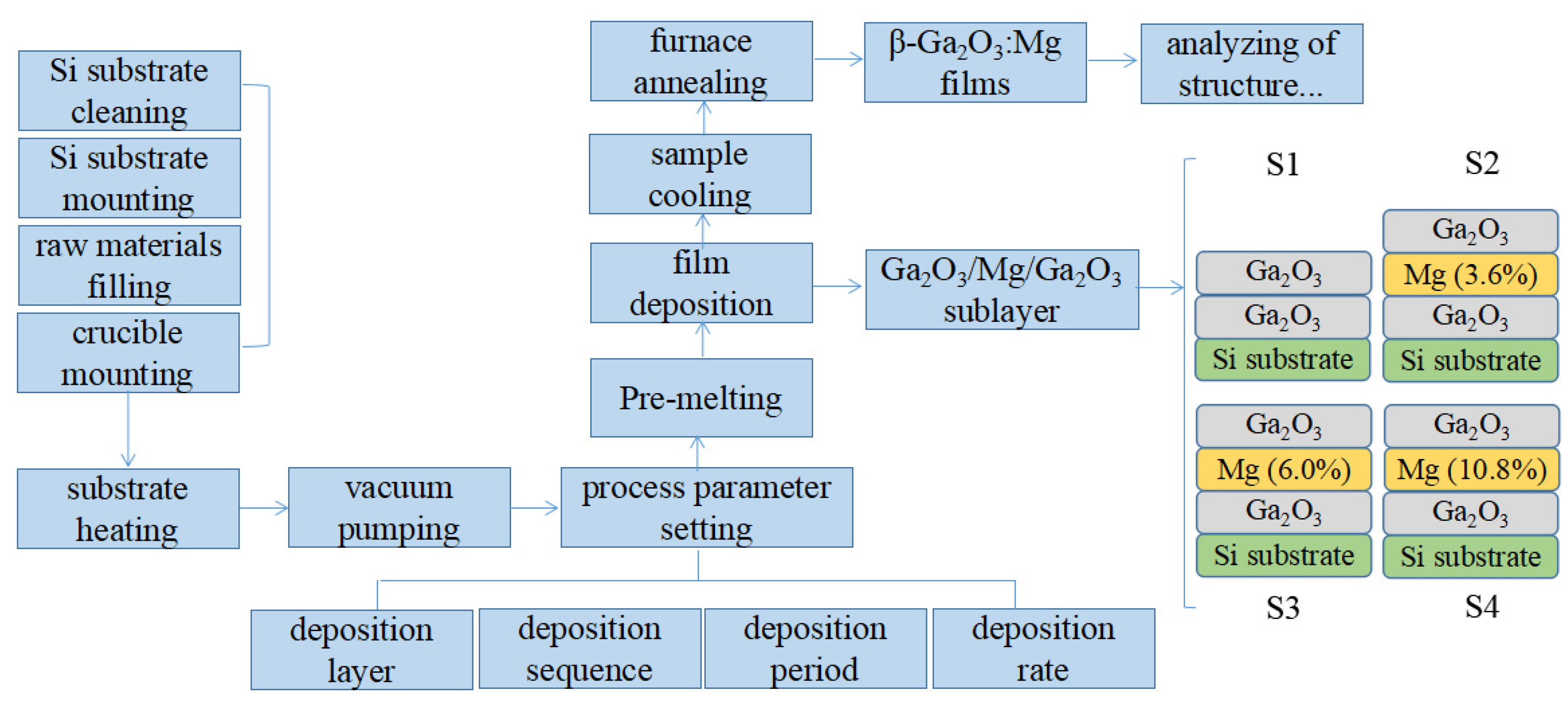
2. Materials and Methods
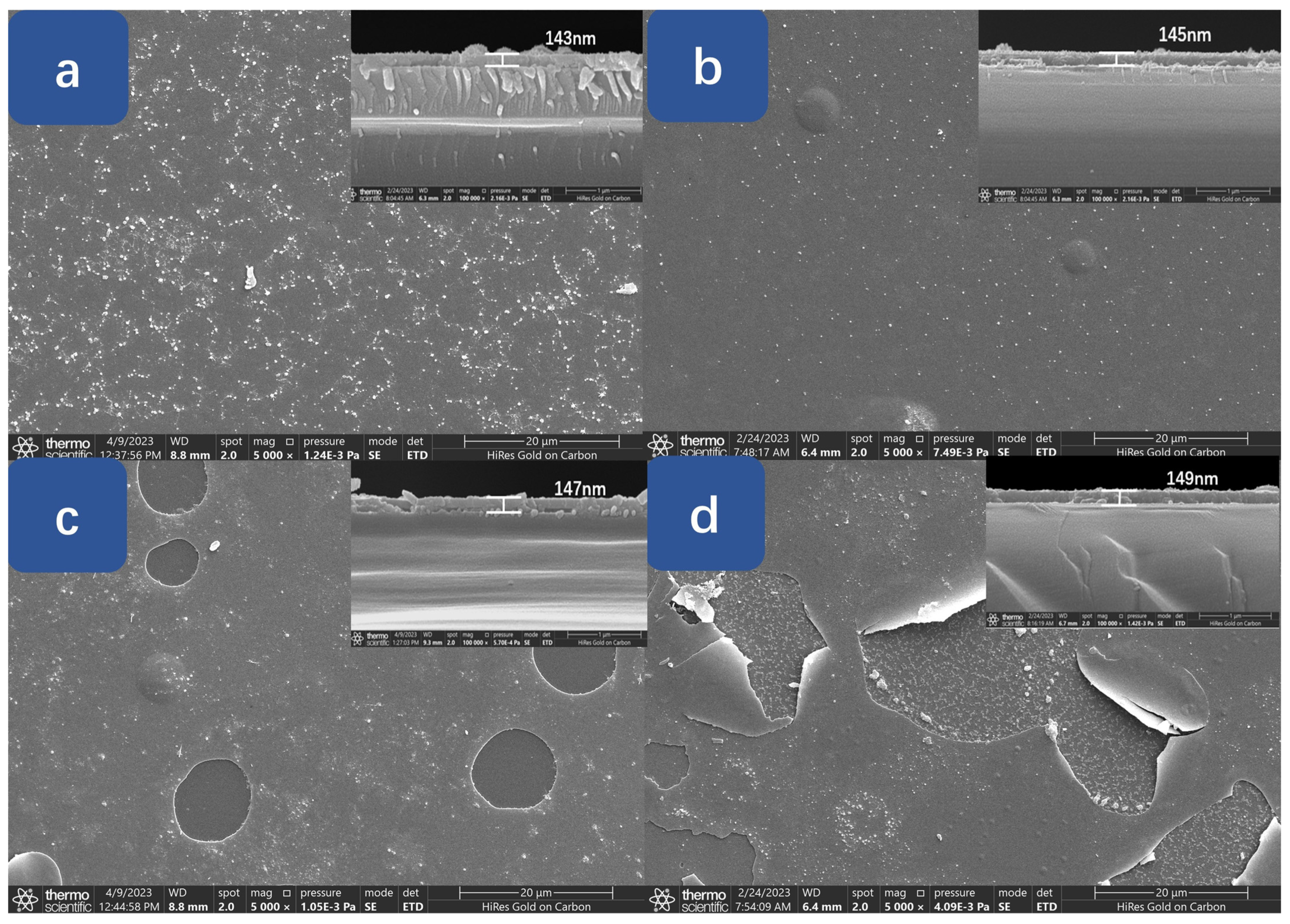
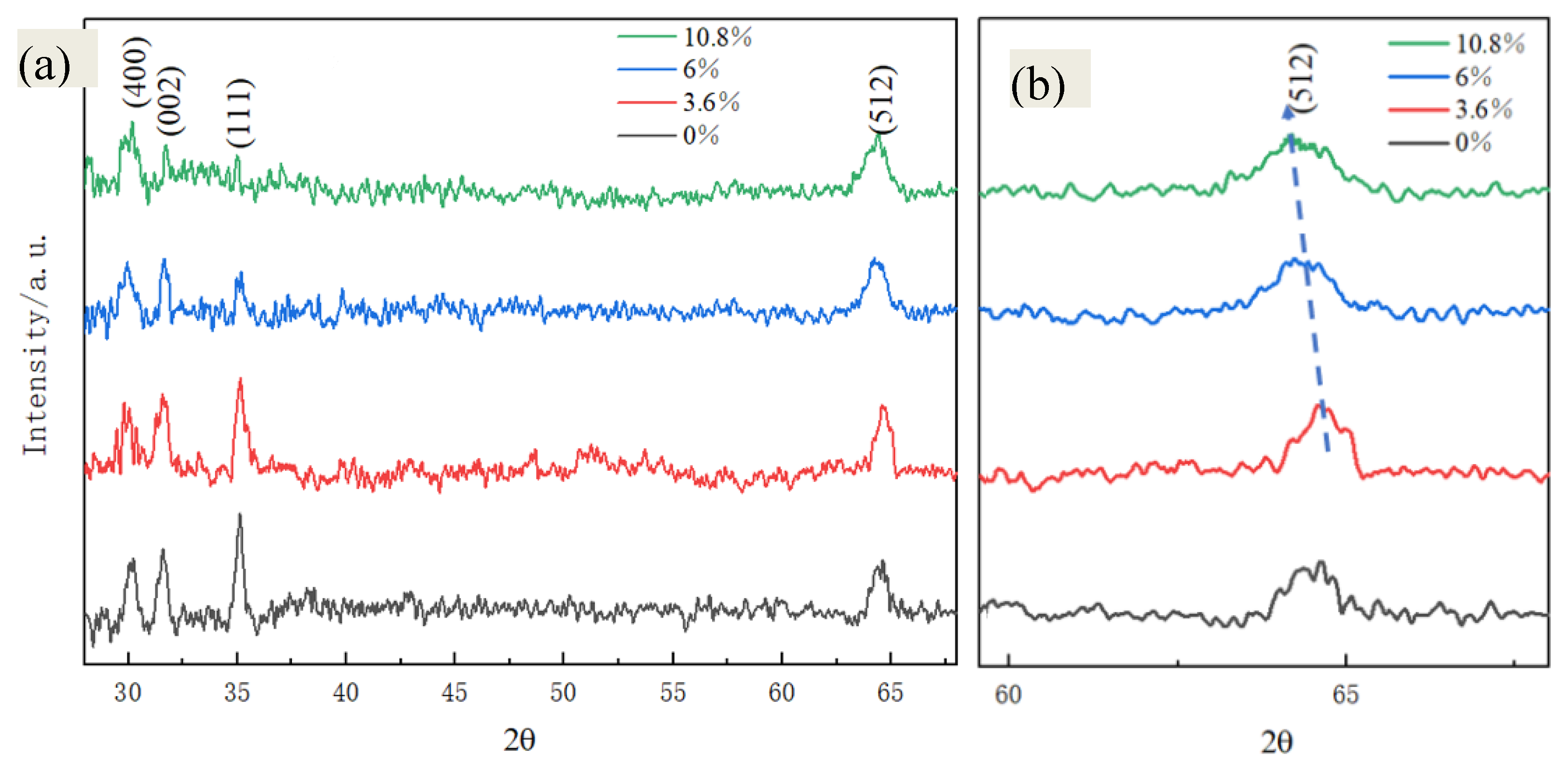
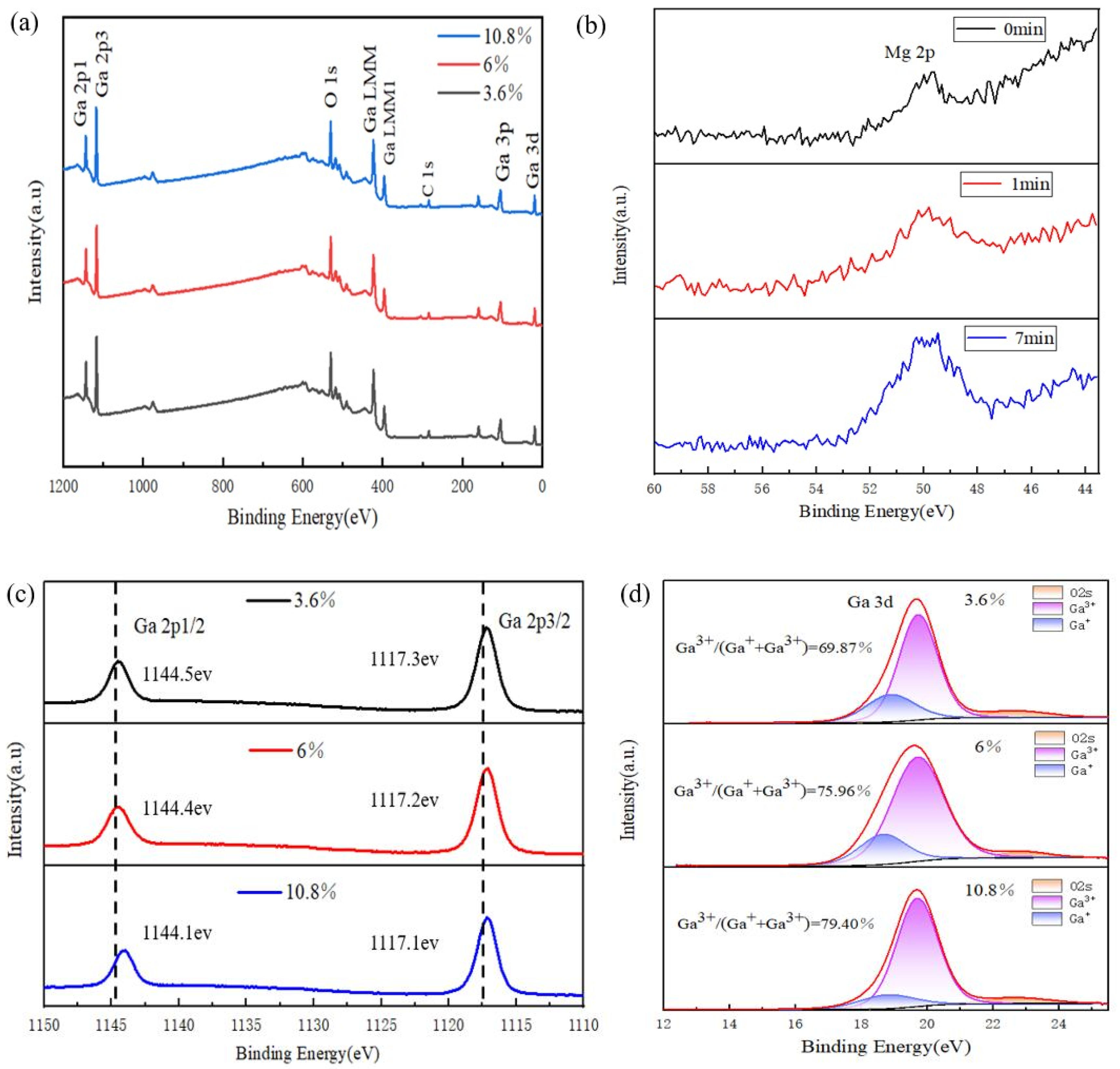
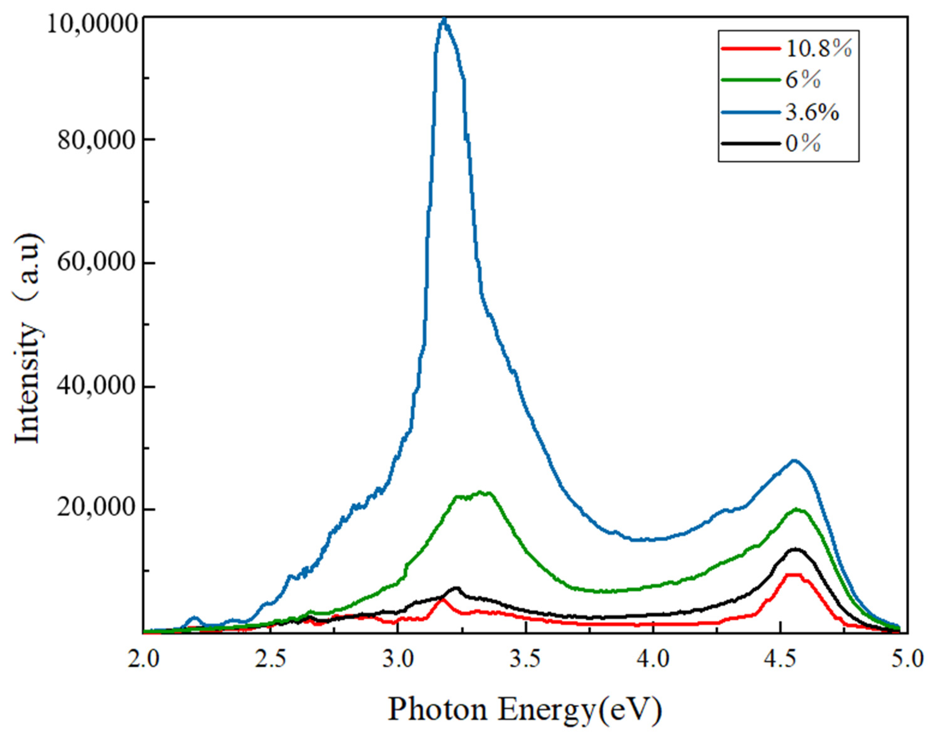
3. Results and Discussion
4. Conclusions
Author Contributions
Funding
Institutional Review Board Statement
Informed Consent Statement
Data Availability Statement
Conflicts of Interest
References
- Ren, W.; Li, X.-M.; Fan, W.-T.; Wang, W.-L.; Li, S.-R.; Liu, X.-H.; Li, N.; Liu, G.-H.; Weng, X. Strain alleviation and light emission improvement of indium-doped β-Ga2O3 films. J. Lumin. 2024, 273, 120685. [Google Scholar] [CrossRef]
- Liu, Z.; Li, P.-G.; Zhi, Y.-S.; Wang, X.-L.; Chu, X.-L.; Tang, W.-H. Review of gallium oxide based field-effect transistors and Schottky barrier diodes. Chin. Phys. B 2019, 28, 017105. [Google Scholar] [CrossRef]
- Lee, S.; Choi, K.; Kang, H. Growth mechanism of In–doped β–Ga2O3 nanowires deposited by radio frequency powder sputtering. Mater. Lett. 2016, 176, 213–218. [Google Scholar] [CrossRef]
- Wang, C.-C.; Lee, B.-C.; Shieu, F.-S.; Shih, H.C. Characterization and photoluminescence of Sn-doped β-Ga2O3 nanowires formed by thermal evaporation. Chem. Phys. Lett. 2020, 753, 137624. [Google Scholar] [CrossRef]
- Skachkov, D.; Lambrecht, W.R.L. Computational study of electron paramagnetic resonance parameters for Mg and Zn impurities in β-Ga2O3. Appl. Phys. Lett. 2019, 114, 202102. [Google Scholar] [CrossRef]
- Islam, M.; Liedke, M.O.; Winarski, D.; Butterling, M.; Wagner, A.; Hosemann, P.; Wang, Y.; Uberuaga, B.; Selim, F.A. Chemical manipulation of hydrogen induced high p-type and n-type conductivity in Ga2O3. Sci. Rep. 2020, 10, 6134. [Google Scholar] [CrossRef]
- Qian, Y.; Guo, D.; Chu, X.; Shi, H.; Zhu, W.; Wang, K.; Huang, X.; Wang, H.; Wang, S.; Li, P.; et al. Mg-doped p-type β-Ga2O3 thin film for solar-blind ultraviolet photodetector. Mater. Lett. 2017, 209, 558–561. [Google Scholar] [CrossRef]
- Feng, X.; Li, Z.; Mi, W.; Luo, Y.; Ma, J. Mg-doped β-Ga2O3 films with tunable optical band gap prepared on MgO (110) substrates by metal-organic chemical vapor deposition. Mater. Sci. Semicond. Process. 2015, 34, 52–57. [Google Scholar] [CrossRef]
- Chu, S.-Y.; Yeh, T.-H.; Lee, C.-T.; Lee, H.-Y. Mg-doped beta-Ga2O3 films deposited by plasma-enhanced atomic layer deposition system for metal-semiconductor-metal ultraviolet C photodetectors. Mater. Sci. Semicond. Process. 2022, 142, 106471. [Google Scholar] [CrossRef]
- Kumar, S.; Singh, R. Nanofunctional gallium oxide (Ga2O3) nanowires/nanostructures and their applications in nanodevices. Phys. Status Solidi (RRL)-Rapid Res. Lett. 2013, 7, 781–792. [Google Scholar] [CrossRef]
- Fan, T.; Tang, N.; Wei, J.; Zhang, S.; Sun, Z.; Li, G.; Jiang, J.; Fu, L.; Zhang, Y.; Yuan, Y.; et al. Reduction of vacancy defects induced by thermal annealing in β-Ga2O3 epilayer. Micro Nanostruct. 2023, 176, 207525. [Google Scholar] [CrossRef]
- Frodason, Y.K.; Johansen, K.M.; Vines, L.; Varley, J.B. Self-trapped hole and impurity-related broad luminescence in β-Ga2O3. J. Appl. Phys. 2020, 127, 075701. [Google Scholar] [CrossRef]
- Kananen, B.E.; Halliburton, L.E.; Scherrer, E.M.; Stevens, K.T.; Foundos, G.K.; Chang, K.B.; Giles, N.C. Electron paramagnetic resonance study of neutral Mg acceptors in β-Ga2O3 crystals. Appl. Phys. Lett. 2017, 111, 072102. [Google Scholar] [CrossRef]
- Lenyk, C.A.; Gustafson, T.D.; Halliburton, L.E.; Giles, N.C. Deep donors and acceptors in β-Ga2O3 crystals: Determination of the Fe2+/3+ level by a noncontact method. J. Appl. Phys. 2019, 126, 245701. [Google Scholar] [CrossRef]
- Sharma, R.; Law, M.E.; Ren, F.; Polyakov, A.Y.; Pearton, S.J. Diffusion of dopants and impurities in β-Ga2O3. J. Vac. Sci. Technol. A Vac. Surf. Film. 2021, 39, 060801. [Google Scholar] [CrossRef]
- Su, Y.; Guo, D.; Ye, J.; Zhao, H.; Wang, Z.; Wang, S.; Li, P.; Tang, W. Deep level acceptors of Zn-Mg divalent ions dopants in β-Ga2O3 for the difficulty to p-type conductivity. J. Alloys Compd. 2019, 782, 299–303. [Google Scholar] [CrossRef]
- Bhandari, S.; Zvanut, M.E. Optical transitions for impurities in Ga2O3 as determined by photo-induced electron paramagnetic resonance spectroscopy. J. Appl. Phys. 2020, 127, 065704. [Google Scholar] [CrossRef]
- Wong, M.H.; Lin, C.-H.; Kuramata, A.; Yamakoshi, S.; Murakami, H.; Kumagai, Y.; Higashiwaki, M. Acceptor doping of β-Ga2O3 by Mg and N ion implantations. Appl. Phys. Lett. 2018, 113, 102103. [Google Scholar] [CrossRef]
- Ren, W.; Han, Y.-X.; Wang, W.-L.; Li, S.-R.; Liu, X.-H.; Weng, X. Aging improvement of Mn–Zn–Ni–Mg–Al–O high-entropy oxide films. J. Mater. Sci. Mater. Electron. 2024, 35, 40. [Google Scholar] [CrossRef]
- Ren, W.; Ding, T.; Wang, W.-L.; Zhang, Y.-X.; Li, Y.; Lu, Y.-T.; Ma, C. Microstructure and cation distribution of Mn2–xAlxZn0.2Ni0.6Mg0.2O4 high entropy oxide films. J. Mater. Sci. Mater. Electron. 2023, 34, 655. [Google Scholar] [CrossRef]
- Li, W.; Zhao, X.; Zhi, Y.; Zhang, X.; Chen, Z.; Chu, X.; Yang, H.; Wu, Z.; Tang, W. Fabrication of cerium-doped β-Ga2O3 epitaxial thin films and deep ultraviolet photodetectors. Appl. Opt. 2018, 57, 538–543. [Google Scholar] [CrossRef]
- Wang, C.; Li, S.-W.; Zhang, Y.-C.; Fan, W.-H.; Lin, H.-J.; Wuu, D.-S.; Lien, S.-Y.; Zhu, W.-Z. Oxygen annealing induced crystallization and cracking of pulsed laser deposited Ga2O3 films. Vacuum 2022, 202, 111176. [Google Scholar] [CrossRef]
- Tanaka, K.; Akiniwa, Y. Diffraction Measurements of Residual Macrostress and Microstress Using X-rays, Synchrotron and Neutrons. JSME Int. J. Ser. A 2004, 47, 252–263. [Google Scholar] [CrossRef]
- Liu, J.; Yang, H.; Tan, W.; Zhou, X.; Lin, Y. Photovoltaic performance improvement of dye-sensitized solar cells based on tantalum-doped TiO2 thin films. Electrochim. Acta 2010, 56, 396–400. [Google Scholar] [CrossRef]
- Nouri, H.; Habibi-Yangjeh, A. Microwave-assisted method for preparation of Zn1−xMgxO nanostructures and their activities for photodegradation of methylene blue. Adv. Powder Technol. 2014, 25, 1016–1025. [Google Scholar] [CrossRef]
- Zhou, B.; Li, Y.; Bai, J.; Li, X.; Li, F.; Liu, L. Controlled synthesis of rh-In2O3 nanostructures with different morphologies for efficient photocatalytic degradation of oxytetracycline. Appl. Surf. Sci. 2018, 464, 115–124. [Google Scholar] [CrossRef]
- Li, P.; Han, X.; Chen, D.; Sai, Q.; Qi, H. Effect of air annealing on the structural, electrical, and optical properties of V-doped β-Ga2O3 single crystals. J. Alloys Compd. 2022, 908, 164590. [Google Scholar] [CrossRef]
- Li, P.; Han, X.; Chen, D.; Sai, Q.; Qi, H. Electrical and optical properties and defects of (100)- and (001)-oriented V-doped β-Ga2O3 crystals grown by EFG. Mater. Sci. Semicond. Process. 2023, 153, 107159. [Google Scholar] [CrossRef]
- Yamaoka, S.; Nakayama, M. Evidence for formation of self-trapped excitons in a β-Ga2O3 single crystal. Curr. Top. Solid State Phys. 2015, 13, 93–96. [Google Scholar] [CrossRef]
- Li, S.; Luo, J.; Liu, J.; Tang, J. Self-Trapped Excitons in All-Inorganic Halide Perovskites: Fundamentals, Status, and Potential Applications. J. Phys. Chem. Lett. 2019, 10, 1999–2007. [Google Scholar] [CrossRef]
- Varley, J.B.; Janotti, A.; Franchini, C.; Van de Walle, C.G. Role of self-trapping in luminescence andp-type conductivity of wide-band-gap oxides. Phys. Rev. B 2012, 85, 081109. [Google Scholar] [CrossRef]

| Sample No. | Peak Position (◦) | Strain ε (10−3) |
|---|---|---|
| S1 (0%) | 64.758 | 1.185 |
| S2 (3.6%) | 64.752 | 1.103 |
| S3 (6%) | 64.721 | 0.675 |
| S4 (10.8%) | 64.698 | 0.358 |
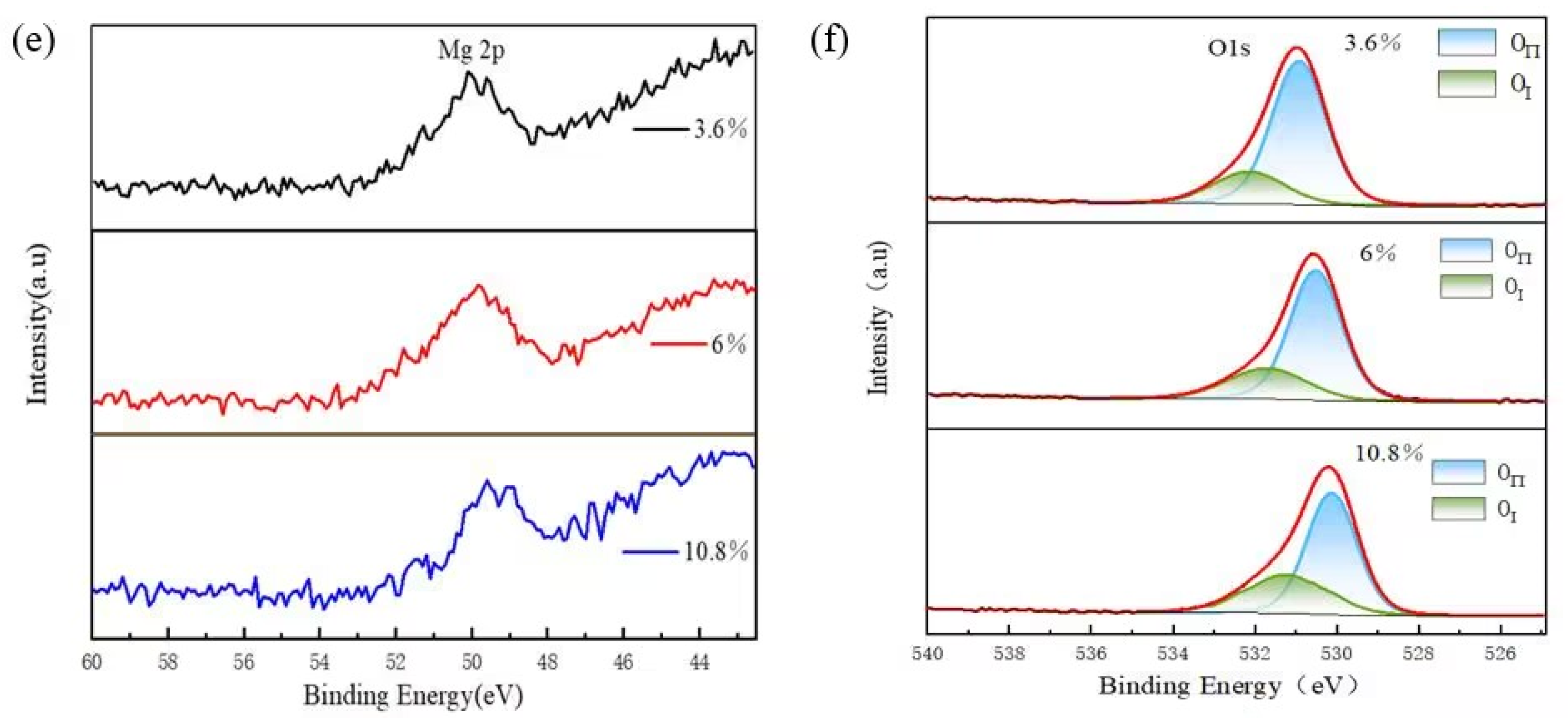
| Sample No. | Ga3+ | Ga+ | OII | OI | Ga3+/(Ga3+ + Ga+) | OII/(OI + OII) |
|---|---|---|---|---|---|---|
| S2 (3.6%) | 0.6987 | 0.3013 | 0.7745 | 0.2255 | 0.6987 | 0.7745 |
| S3 (6%) | 0.7596 | 0.2404 | 0.7285 | 0.2715 | 0.7596 | 0.7285 |
| S4 (10.8%) | 0.794 | 0.2006 | 0.6264 | 0.3736 | 0.7983 | 0.6264 |
Disclaimer/Publisher’s Note: The statements, opinions and data contained in all publications are solely those of the individual author(s) and contributor(s) and not of MDPI and/or the editor(s). MDPI and/or the editor(s) disclaim responsibility for any injury to people or property resulting from any ideas, methods, instructions or products referred to in the content. |
© 2024 by the authors. Licensee MDPI, Basel, Switzerland. This article is an open access article distributed under the terms and conditions of the Creative Commons Attribution (CC BY) license (https://creativecommons.org/licenses/by/4.0/).
Share and Cite
Fan, W.; Li, S.; Ren, W.; Yang, Y.; Li, Y.; Liu, G.; Wang, W. Synthesis of β-Ga2O3:Mg Thin Films by Electron Beam Evaporation and Postannealing. Materials 2024, 17, 4931. https://doi.org/10.3390/ma17194931
Fan W, Li S, Ren W, Yang Y, Li Y, Liu G, Wang W. Synthesis of β-Ga2O3:Mg Thin Films by Electron Beam Evaporation and Postannealing. Materials. 2024; 17(19):4931. https://doi.org/10.3390/ma17194931
Chicago/Turabian StyleFan, Weitao, Sairui Li, Wei Ren, Yanhan Yang, Yixuan Li, Guanghui Liu, and Weili Wang. 2024. "Synthesis of β-Ga2O3:Mg Thin Films by Electron Beam Evaporation and Postannealing" Materials 17, no. 19: 4931. https://doi.org/10.3390/ma17194931
APA StyleFan, W., Li, S., Ren, W., Yang, Y., Li, Y., Liu, G., & Wang, W. (2024). Synthesis of β-Ga2O3:Mg Thin Films by Electron Beam Evaporation and Postannealing. Materials, 17(19), 4931. https://doi.org/10.3390/ma17194931