Article

A Broadband Photodetector Based on Non-Layered MnS/WSe2 Type-I Heterojunctions with Ultrahigh Photoresponsivity and Fast Photoresponse

Guangdong Provincial Key Laboratory of Information Photonics Technology, Guangdong Provincial Key Laboratory of Functional Soft Condensed Matter, School of Material and Energy, Guangdong University of Technology, Guangzhou 510006, China
*
Authors to whom correspondence should be addressed.
These authors contributed equally to this work.
Materials 2024, 17(7), 1590; https://doi.org/10.3390/ma17071590
Submission received: 21 February 2024 / Revised: 27 March 2024 / Accepted: 28 March 2024 / Published: 30 March 2024

Abstract

:
The separation of photogenerated electron–hole pairs is crucial for the construction of high-performance and wide-band responsive photodetectors. The type-I heterojunction as a photodetector is seldomly studied due to its limited separation of the carriers and narrow optical response. In this work, we demonstrated that the high performance of type-I heterojunction as a broadband photodetector can be obtained by rational design of the band alignment and proper modulation from external electric field. The heterojunction device is fabricated by vertical stacking of non-layered MnS and WSe2 flakes. Its type-I band structure is confirmed by the first-principles calculations. The MnS/WSe2 heterojunction presents a wide optical detecting range spanning from 365 nm to 1550 nm. It exhibits the characteristics of bidirectional transportation, a current on/off ratio over 103, and an excellent photoresponsivity of 108 A W−1 in the visible range. Furthermore, the response time of the device is 19 ms (rise time) and 10 ms (fall time), which is much faster than that of its constituents MnS and WSe2. The facilitation of carrier accumulation caused by the interfacial band bending is thought to be critical to the photoresponse performance of the heterojunction. In addition, the device can operate in self-powered mode, indicating a photovoltaic effect.

1. Introduction

In recent years, ultra-thin two-dimensional (2D) nanomaterials have attracted extensive attention due to their unconventional physical and chemical properties [1,2]. In particular, 2D material heterojunctions with atomically sharp heterointerfaces, adjustable energy band alignments, and attractive interlayer couplings [3,4,5] have emerged as important components in nanoelectronic and optoelectronic devices [6,7,8,9,10]. In particular, the band alignments of 2D heterojunctions affect the transport of photogenerated carriers, which is crucial for the construction of high-performance and wide-band responsive photodetectors. Most photodetectors are based on the building block of heterojunctions possessing type-II band alignment on account of the efficient separation of electron–hole pairs generated in either component [11,12,13]. In this band structure, the conduction band minimum (CBM) and valence band maximum (VBM) of a type-II heterojunction are separately located in its two different components, whereas, for a type-I heterojunction, both the CBM and VBM are located in the narrow bandgap side, which becomes the potential well for photogenerated carriers. In this case, either electrons or holes generated in the barrier side can be injected into the well side through the heterointerface, and the opposite carriers are collected on the electrode of barrier side, while carriers generated in the well side cannot be effectively separated due to the energy barriers at the interface. Therefore, photodetectors based on a type-I heterojunction show spectral response selectively decided by the barrier component, which usually corresponds to ultraviolet (UV) or visible range. The effective separation of photogenerated electron–hole pairs in type-I band alignment is proved to be very helpful to realize ultrafast and sensitive photodetection [14]. However, taking full advantage of improving carrier collection efficiency, the broadband response based on a type-I heterojunction is still a challenge.
Fortunately, properly designed heterojunctions can break through the limitations of the material itself to work in UV to visible or even near-infrared band [15]. The conduction and valence band offsets as well as the band bending are determined by the properties of components, and can be synchronously modulated by electric field. Therefore, rational designs of the type-I band alignment and carrier transport process with electric field modulation are crucial for constructing novel photodetectors based on type-I heterojunctions with broadband response and efficient carrier separation. Compared with type-II heterojunctions, which are widely studied and fabricated, type-I heterojunctions are less studied, and the optical response principle and regulation mechanism are not fully understood. Hence, it is highly desirable to design and fabricate a novel type-I heterojunction, analyze its tunable band alignment modulated by electric field, and investigate its optoelectronic performance as a photodetector.
The emergence of 2D non-layered materials with three-dimensional chemically bonded crystal structures not only greatly extends the scope of the inherent layered 2D materials, but also demonstrates a range of interesting properties due to the large number of unsaturated dangling bonds on the surface. These surface active sites make them ideal materials for surface active applications such as catalysts [16], supercapacitors [17], and photodetectors [18,19]. As an important member of the group of non-layered materials, MnS, the group VIIB transition metal chalcogenide, exhibits excellent electronic, photoelectric, and magnetic properties [20,21]. The self-containing manganese vacancy in α-MnS (stable rock-salt-type structure) acts as a receptor, resulting in p-type conductive behavior with a wide band gap of 2.7 eV [22,23]. The synthesized α-MnS crystals show excellent photoresponsivity, environmental stability, and flexibility, which indicates that MnS has considerable application potential in flexible electronic and optoelectronic devices [23]. The wide band gap of MnS has benefits in its application in the UV photoresponse [24]. In order to construct the type-I heterojunction based on MnS with a broadband photoresponse, a narrow band gap material is needed as the well layer. WSe2 has an indirect band gap of 0.9–1.6 eV, and the heterojunction detector based on WSe2 shows a broad spectral response ranging from visible and near-infrared light. In addition, the WSe2 field-effect transistor exhibits high carrier mobility (70.1 cm2V−1s−1) and ON/OFF current ratio (over 106) [25,26,27]. Accordingly, heterojunctions formed by stacking WSe2 and other 2D materials will help to broaden the response band and improve the photoresponse performance.
In this work, non-layered MnS grown by chemical vapor deposition (CVD) and mechanically exfoliated WSe2 were used to construct the 2D heterojunction. Type-I band alignment of the MnS/WSe2 heterojunction was verified by first-principles calculations. The MnS/WSe2 heterojunction exhibits excellent photoresponsive properties and tunable band alignment under electric field modulation. The device also shows the characteristic of bidirectional transportation. The influence of carrier accumulation and depletion state at the interface on the photoresponse performance of the device under the two bias cases is discussed. The photodetector based on MnS/WSe2 possesses a broadband detection, a high photoresponsivity, and a fast response speed in the visible light range, which is better than the performance of a single component material (WSe2 or MnS). Furthermore, the photovoltaic effect of the device has been evaluated.

2. Materials and Methods

2.1. Synthesis of MnS Nanosheets

The mica substrate was ultrasonically treated in ethanol, acetone, and isopropyl alcohol for 15 min to remove organic pollutants before the preparation of MnS nanosheets. The whole preparation process was executed in a two-temperature zone CVD system. The precursors were S powder (99.98%, Alfa, Shanghai, China) and the mixed powder of high purity MnCl2 powder (99.999%, Alfa, Shanghai, China) with some NaCl. S powder and the mixed powder were separately placed in two quartz boats in the middle of the high temperature region and low temperature zone of the furnace, respectively. The temperature in the high temperature region was maintained at 640~660 °C, and the low temperature region was maintained at 180 °C. The mica substrate was placed on a quartz sheet about 5 cm from the MnCl2/NaCl powder at the downstream end of the high temperature zone. Before heating, 200 sccm Ar (96%) and H2 (4%) mixture was injected into the tube for 30 min to remove O2, which ensured a stable reaction environment. Then, heating the furnace to the required growth temperature, a MnS nanosheet was grown for 5–10 min with a continuous flow of 20–30 sccm under normal pressure. Finally, the heating was stopped, and the flow rate was increased to 100 sccm. The mica substrate was naturally cooled to normal temperature.

2.2. Preparation of WSe2 Nanosheets

WSe2 nanosheets were mechanical exfoliated from the commercial bulk WSe2 (ONWAY, Shanghai, China) on blue tape (NITTO, Hongkong, China) and transferred to the Si/SiO2 substrate.

2.3. Characterizations

Optical microscope (Motic, Xiamen, China) was used to characterize the morphology. Material composition was characterized by X-ray photoelectron spectroscopy (XPS) (Thermo Fisher, Waltham, MA, USA). X-ray diffraction (XRD) (Bruker, Bilerika, MA, USA) and high-resolution transmission electron microscopy (HRTEM) (FEI, Hillsboro, OR, USA) were applied to characterize microstructure. The electric and photoelectric properties were studied on a four-probe table (SEMISHARE, Shenzhen, China) combined with the 2636B source meter (KEITHLEY, Cleveland, OH, USA). For this, 365, 405, 532, 808, and 1550 nm lasers were applied as the probing light sources.

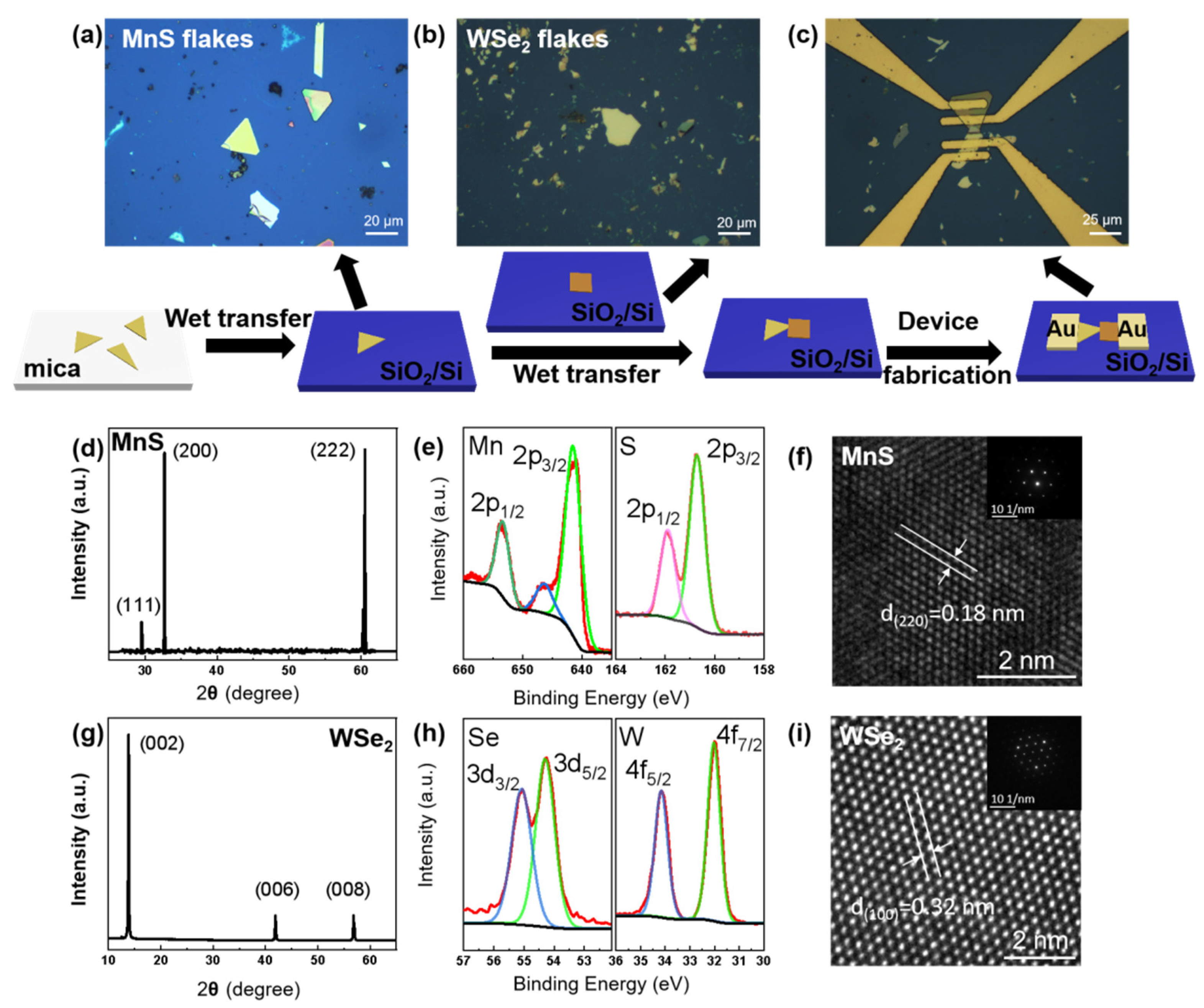
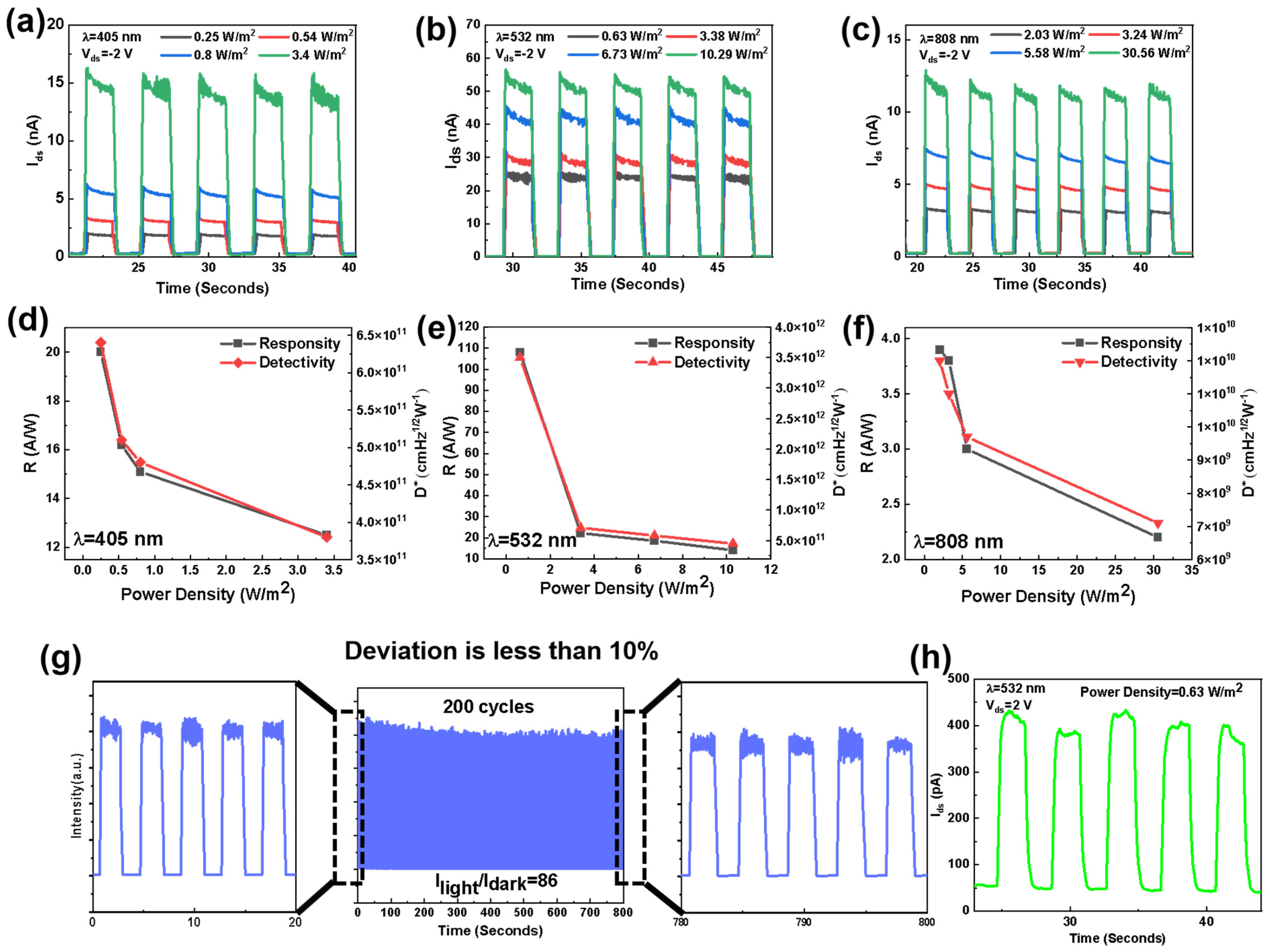
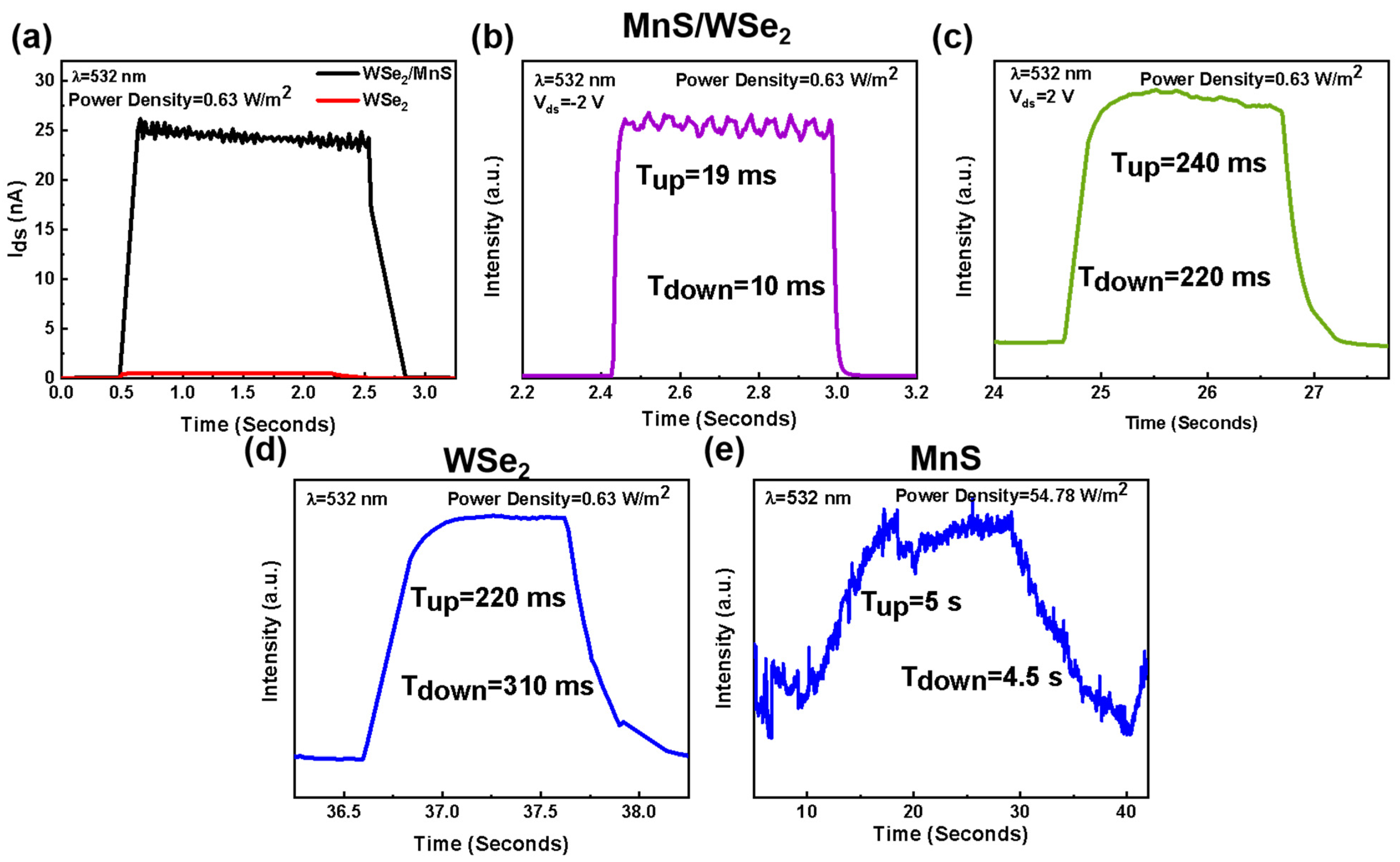
3. Results and Discussion

Two-dimensional MnS flakes were grown on mica substrates by the CVD method and then were transferred onto the SiO2 (300 nm)/Si substrate through the wet transfer process. WSe2 was removed by a mechanical exfoliation method and transferred onto the above SiO2/Si substrate. Then, MnS and WSe2 were used to constitute a vertical stack junction through the wet transfer process. After that, 50 nm Au was used to cover the MnS/WSe2 heterojunction by a standard lithography process and electron beam evaporation. The above preparation method is shown in Figure 1a–c and the detailed preparation process is in the e.g., Section 2.
The constituent materials and microstructure of the heterojunction are characterized by XRD, XPS, and HRTEM. The formation of pure MnS crystals and their single-crystal nature are confirmed by the XRD result, as shown in Figure 1d. The XRD peaks appear at positions of 2θ = 29.5°, 32.7°, and 60.5°, corresponding to the (111), (200), and (222) planes of MnS, which is well-conformed with the criterion MnS pattern (PDF no. 06-0518). In Figure 1e, the XPS spectrum exhibits that peak positions at 653.5 eV and 641.4 eV belong to Mn 2p1/2 and Mn 2p3/2, respectively. Those at 161.9 eV and 160.7 eV are designated as S 2p1/2 and S 2p3/2 [28]. As shown in Figure 1f, the HRTEM image of MnS exhibits a (220) crystal plane with a spacing of 0.18 nm, matching the description with the XRD result. In the inset of Figure 1f, the SAED pattern exhibits one set of hexagonal diffraction spots, indicating the high quality of the MnS single crystal. As shown in Figure 1g, the major XRD peaks appear at positions of 2θ = 13.8°, 41.8°, and 56.8°, corresponding to the (002), (006), and (008) planes of WSe2, which is well-matched to the standard WSe2 pattern (PDF no. 38-1388). The peaks at 34.1 eV and 32.0 eV in Figure 1h are assigned to W 4f5/2 and W 4f7/2, respectively, while the other two peaks at 55.1 eV and 54.3 eV are designated as Se 3d3/2 and Se 3d5/2 states of WSe2 [29], respectively. As shown in Figure 1i, the spacing of WSe2 is 0.32 nm in the HRTEM image, corresponding to the WSe2 (100) plane. The SAED pattern in the inset of Figure 1i shows one set of hexagonal diffraction spots, indicating the high quality of the WSe2 single crystal.
As shown in Figure 2a, the thicknesses of the MnS and WSe2 nanosheets are studied by AFM and calculated to be 100 and 40 nm, respectively. The conductivity type of MnS is experimentally measured as p-type, shown in Supplementary Figure S1, and WSe2 is measured as bipolar conductivity [30]. Then, as shown in Figure 2b, the built-in contact potential difference at the interface between MnS and WSe2 is obtained by Kelvin probe force microscopy (KPFM) measurement. To illustrate the surface potential distribution (SPD) of MnS and WSe2 nanosheets with respect to the tip region of AFM, the following equations can be expressed:
e S D P M n S = W t i p W M n S
e S D P W S e 2 = W t i p W W S e 2
where e is the electron charge, and W t i p , W M n S , and W W S e 2 are the work functions of the AFM tip, MnS, and WSe2 flakes, respectively. In order to obtain the Fermi energy level difference ΔEF between MnS and WSe2, the following equation is expressed:
E F = W M n S W W S e 2 = e S D P M n S e S D P W S e 2
As shown in Figure 2c, the work function difference between MnS and WSe2 is about 0.16 eV. W M n S and W W S e 2 are about 4.7 and 4.54 eV, respectively, by calculation through W t i p as 4.5 eV. The band diagrams of MnS and WSe2 are obtained by the first-principles calculations. The calculations are performed using the projector-augmented plane-wave (PAW) method within the work of density functional theory (DFT) in the VASP software package (VASP 5.4). The generalized gradient approximation (GGA) of Perdew, Burke, and Ernzerhof (PBE) function is employed for the electron exchange and correlation [31]. A vacuum of about 20 Å is applied to eliminate the interaction between adjacent images. The cutoff energy of the plane-wave basis set is 450 eV. The first Brillouin zone is sampled with a (15 × 15 × 1) Monkhorst−Pack grid for the relaxation of MnS and WSe2. All of the structures are fully relaxed with a force tolerance of 0.02 eV/Å. In addition, 1 × 1 supercells with 1~4 layers of both MnS and WSe2 are constructed, as shown in Supplementary Figure S2a–e. The average band offsets of CBM and VBM between MnS and WSe2 are 0.25 eV and 0.68 eV, respectively, and the band alignments of MnS and WSe2 before contact with ΔEF of 0.16 eV is shown in Figure 2c. Finally, taking Fermi energy level difference into consideration, the MnS/WSe2 heterojunction still shows a type-I band structure with a built-in electric field from WSe2 to MnS, as shown in Figure 2d.
Applied bias on the MnS/WSe2 field-effect transistor (FET) is demonstrated in Figure 3a, with MnS as source and WSe2 as the drain electrodes. To further investigate the electrical characteristics of the device as shown in Figure 3b,c, the analysis combined with band alignments is conducted as shown in Figure 3d–f. The tunable band alignment and carrier transport process under electric field modulation can be divided into the following three processes described below.
When forward bias (0 V < Vds < 2 V) is applied, electrons in the WSe2 conduction band cannot normally move towards the drain electrode due to the high potential barrier of MnS, while holes in the MnS valence band can move towards the source electrode. The band bending at the interface forms a hole depletion region on the MnS side and an electron depletion region on the WSe2 side, which hinders carrier transport in forward bias. These explain the low dark current under 0–2 V bias in the Ids–Vds curve, as shown in Figure 3b.
When Vds is greater than 2 V, the current increases rapidly as the forward bias continues to increase because the electron barrier no longer exists, due to the energy band upward shift of WSe2. Therefore, the electrons in WSe2 can transfer to the drain electrode and the holes in the MnS valence band can move towards the source electrode.
Under reverse bias, with the energy band of WSe2 moving down, electrons in the MnS conduction band can move easily toward the source electrode, and the confinement effect of holes in the WSe2 valence band gradually weakens until the VBM of WSe2 is lower than of the VBM of MnS. Consequently, holes in the WSe2 valence band can transfer toward the drain electrode, and the heterojunction presents a state of reverse conduction. This explains the Ids–Vds curve where the current increases when the voltage of Vds is less than 0 V.
The Ids–Vds curve in Figure 3b shows the bidirectional transport characteristics of the MnS/WSe2 heterojunction, and the reverse current is greater than the forward current at ±2 V. The voltage direction coinciding with the internal electric field increases the interface band bending, which results in the strengthened accumulation regions of electrons on the MnS side and holes on the WSe2 side. The situation better matches and facilitates carrier transport under reverse bias. The ambipolar behavior of the heterojunction is confirmed by transfer characteristic curve from Figure 3c. However, p-type characteristics dominate, explaining that the electrical conductivity of the device is mainly governed by the MnS channel. It can be seen from Figure 3c that the current on/off ratio of the device exceeds 103.
The photoresponse performance of the heterojunction device is systematically investigated. As shown in Figure 4a–c, the photocurrent of the device is measured at Vds = −2 V and under the probing light of 405, 532, and 808 nm lasers, respectively. The three parameters that evaluate the optical response performance of a device are responsivity (Rλ), detectivity (D*), and external quantum efficiency (EQE). The photocurrent generated per unit power of the incident light per unit area of a photoelectric device is the responsivity Rλ. The equation is expressed as follows
R λ = I p h P λ A = I l i g h t I d a r k P λ A
where Ilight and Idark are the photocurrents in light and dark conditions, respectively, and Pλ is illumination power density. The effectively irradiated area of the device is A. D* determines the capacity to detect weak optical signals [32,33,34] and is expressed as follows
D * = R λ A S n
where e is the charge of electron and Sn is the noise spectral density. The number of electron–hole pairs excited by one incident photon is defined as EQE. The expression is as follows
E Q E = h c R λ e λ
where h is Planck constant and λ is the incident wavelength. As shown in Figure 4d–f, the responsivity and detectivity under different optical power densities of 435, 532, and 808 nm lasers are calculated. As shown in Figure 4b,e, under the 532 nm laser with a power density of 0.63 W m−2, the photocurrent is 2.56 × 10⁸ A and the dark current is 2.17 × 10¹⁰ A. Fourier transform of the dark current traces gives the noise spectral density (Sn) as a function of frequency, as shown in Figure S4. Considering the fast speed of the device, Sn can be extracted at a frequency of 20 Hz. The calculated maximal Rλ, D*, and EQE are 108 A W−1, 3.5 × 10¹² jones, and 25,100%, respectively. To comprehend the relationship between optical power density and optical response, the power-law Iph ∝ Pα (α is the power index) is used to define the photocurrent. The fitted function relationship between photocurrent and optical power density is Iph (A) ∝ 2.5 × 10⁸ [P(W/m2)]0.79. Furthermore, in order to study the stability, the device was irradiated for 200 consecutive cycles under a 532 nm laser. The optical switching of the device exhibits a steady response and only a slight attenuation of the photocurrent (deviation less than 10%) in Figure 4g. These results indicate that the MnS/WSe2 heterojunction has the potential for high-performance photoelectric detection.
The photoresponse performance of the heterojunction device measured at Vds = 2 V and under the irradiation of 532 nm laser is also investigated, as shown in Figure 4h. The maximal Rλ is 0.34 A W−1 under forward bias, which is lower than that under reverse bias. It reveals the influence of carrier accumulation and depletion state at the interface on the photoresponse performance of the device.
Except for the visible region, the light response for UV and near-infrared is studied subsequently, as shown in Figure 5a–d. When the 365 nm laser with a power density of 0.32 W m−2 illuminates the device, three parameters (Rλ, D*, and EQE) are calculated to 0.78 A W−1, 2.5 × 10¹⁰ jones, and 260%, respectively. The heterojunction also generates a photocurrent under a 1550 nm laser with 13.41 W m−2. By calculation, Rλ, D*, and EQE are 1.09 mA W−1, 3.2 × 10⁷ jones, and 7.9%. The resulting photocurrent is relatively low. The downward pulling of the WSe2 side band diagram forms a type-II band alignment under the reverse bias, as shown in Figure S3, which allows the photogenerated holes in WSe2 to transport directly into the VBM of MnS under the 1550 nm laser.
To compare the properties of the heterojunction with its components, the photocurrents from the MnS/WSe2 heterojunction and individual materials of the same device are measured. The photocurrent of MnS/WSe2 heterojunction is nearly 50 times higher than WSe2 in Figure 6a, indicating that the separation of photogenerated electron–hole pairs in the type-I heterostructure effectively improves the optical responsivity. Meanwhile, the response time of the device, MnS, and WSe2 are measured (rising time Tup and falling time Tdown are defined as the interval between the response going up from 10% to 90% and down from 90% to 10%, respectively) in Figure 6b–d. The rising time is 19 ms and falling time is 10 ms, which are two and one order of magnitude faster than MnS (5 s/4.5 s) and WSe2 (220 ms/310 ms), respectively. The band offset leads to photo-generated charge carrier (electron–hole pairs generated by light) separation at the heterojunction interface, thereby accelerating the transport speed of the charge carriers, and the response rate of the heterojunction is faster than that of the simple substance. Even after the 200 cycles shown in Figure 4g, there is almost no change in response time of the heterojunction. The response time of the heterojunction device at Vds = 2 V, is 240 ms (rise time) and 220 ms (fall time), as shown in Figure 6c. It can be seen that, although the carrier separation efficiency of the heterojunction under forward bias is not as good as that under reverse bias, the heterojunction still generates an effective carrier separation with the forward bias modulation. Some key performances of reported broadband photodetectors are collected in Table S2, and it can be seen that the MnS/WSe2 heterojunction has great application potential.
The photovoltaic performance of the device is researched under the zero-bias state. As shown in Figure 7a, when between bias and illuminated, the heterojunction exhibits obvious light response at zero bias, illuminated by a 532 nm laser with the power density of 6.73 W m−2. The short-circuit current (Isc) and open-circuit voltage (Voc) in Figure 7a are 15 pA and 0.17 V, respectively. By calculating the corresponding power of 0–0.17 V, it is concluded that P is the maximum when V = 0.053 V, which is the gray area in the figure (Pmax = 0.9 pW). The fill factor (FF) is the important parameter for assessing the photovoltaic performance. It can be calculated as follows
F F = P m a x V o c I s c
which is calculated to be 0.36. Figure 7b–e shows the device-generated photocurrents under irradiation of 405, 532, 635, and 808 nm lasers with different powers. This indicates the device works as a self-powered photodetector. The strongest light response is generated when the laser is 532 nm with 0.54 W m−2, and the corresponding photo and dark current are 3 pA and 0.1 pA, respectively. Rλ, D*, and EQE are calculated as 9.7 mA W−1, 1.5 × 10⁷ jones, and 22.5%, respectively. It proves that the MnS/WSe2 heterojunction is a well-performing, self-powered photodetector and photovoltaic device. Under the zero-bias state, the wide-bandgap MnS in the type-I structure is the potential barrier both for electrons and holes, which means only the photogenerated carriers in MnS can pass the heterointerface. Thus, the photoresponse of this type-I heterojunction depends on the wide-bandgap material MnS. As the wavelength increases, photon energy is less than the energy required to pass through the MnS band gap; accordingly, the contribution of MnS to the photoresponse gradually decreases, resulting in a gradually smaller photocurrent. In contrast, the optical response characteristics of the device under reverse bias are different, which illustrates that the band alignment and carrier transport process of the type-I MnS/WSe2 heterojunction is tunable under electric field modulation.

4. Conclusions

In summary, WSe2 prepared by a mechanical tape exfoliation method and non-layered MnS grown by CVD are transferred to SiO2(300 nm)/Si substrate by a wet transfer process to constitute vertical structures, and an FET photodetector based on the MnS/WSe2 heterojunction is prepared by standard lithography process. The heterostructure is characterized by XPS, XRD, and HRTEM. The type-I band structure of the MnS/WSe2 heterojunction is confirmed by the first-principles calculations. The potential barrier height is regulated by the external electric field, which enables the efficient separation of photogenerated carriers. Consequently, the recombination of photogenerated carriers in the wideband system is inhibited due to the modulated band alignment, and the carrier collection efficiency is significantly improved, which is conducive to the realization of high-performance light detection. Finally, the heterojunction device exhibits a current on/off ratio over 103 and an excellent photoresponsivity of 108 A W−1 in the visible range, and it can respond in UV–visible–near-infrared band with a fast response speed. The facilitation of carrier accumulation caused by the interface band bending on photoresponse performance has also been proved. In addition, the heterojunction can work in self-power mode and exhibits a photovoltaic effect. It is demonstrated that the 2D non-layered MnS/WSe2 type-I heterojunction exhibits promising application prospects in broadband response photodetectors and photovoltaic devices. This work is instructive for the rational design and modulation of type-I band structures to fabricate high-performance electronic and optoelectronic devices based on 2D non-layered materials.

Supplementary Materials

The following supporting information can be downloaded at: https://www.mdpi.com/article/10.3390/ma17071590/s1, Figure S1: (a) Optical micrograph of device using MnS nanosheets. (b) The Ids–Vds curve of the MnS at Vgs = 0 V. (c) The transfer (Ids–Vgs) curve of MnS at Vds = 2 V. Figure S2: (a–d) Band alignments of MnS and WSe2 with 1~4 layers before contact. (e) The band offsets of CBM and VBM between MnS and WSe2 with 1~4 layers. Figure S3: Under the reverse bias, separation of electron–hole pairs in energy bands under the irradiation of 1550 nm laser. Figure S4: Noise spectral density as a function of frequency at Vds = −2 V, Vgs = 0 V. Table S1: Properties of heterojunction MnS and WSe2. Table S2: The performance of broadband photodetector based on 2D heterojunctions. References [35,36,37,38,39] are cited in the Supplementary Materials.

Author Contributions

Conceptualization, C.X. and X.C.; methodology, Y.Y.; formal analysis, C.X. and S.C.; investigation, C.X.; data curation, C.X.; writing—original draft preparation, C.X.; writing—review and editing, Y.Y., K.L., S.C. and Y.Z.; project administration, S.C. and Y.Z. All authors have read and agreed to the published version of the manuscript.

Funding

This work was sponsored by the National Natural Science Foundation of China (grant no. 61975036) and the Fund of Guangdong Provincial Key Laboratory of Information Photonics Technology (grant no. 2020B121201011).

Institutional Review Board Statement

Not applicable.

Informed Consent Statement

Not applicable.

Data Availability Statement

Data are contained within the article.

Acknowledgments

The authors wish to thank Wei Song and Yu Chen from the Analysis and Test Center, Guangdong University of Technology, for the phase and morphology analysis of the specimens.

Conflicts of Interest

The authors declare no conflicts of interest.

References

  1. Zavabeti, A.; Jannat, A.; Zhong, L.; Haidry, A.A.; Yao, Z.J.; Ou, J.Z. Two-Dimensional Materials in Large-Areas: Synthesis, Properties and Applications. Nano-Micro Lett. 2020, 12, 34. [Google Scholar] [CrossRef] [PubMed]
  2. Novoselov, K.S.; Mishchenko, A.; Carvalho, A.; Castro Neto, A.H. 2D materials and van der Waals heterostructures. Science 2016, 353, aac9439. [Google Scholar] [CrossRef] [PubMed]
  3. Chakraborty, S.K.; Kundu, B.; Nayak, B.; Dash, S.P.; Sahoo, P.K. Challenges and opportunities in 2D heterostructures for electronic and optoelectronic devices. iScience 2022, 25, 103942. [Google Scholar] [CrossRef] [PubMed]
  4. Rivera, P.; Schaibley, J.R.; Jones, A.M.; Ross, J.S.; Wu, S.F.; Aivazian, G.; Klement, P.; Seyler, K.; Clark, G.; Ghimire, N.J.; et al. Observation of long-lived interlayer excitons in monolayer MoSe2-WSe2 heterostructures. Nat. Commun. 2015, 6, 6242. [Google Scholar] [CrossRef] [PubMed]
  5. Jin, C.H.; Kim, J.; Suh, J.; Shi, Z.W.; Chen, B.; Fan, X.; Kam, M.; Watanabe, K.; Taniguchi, T.; Tongay, S.; et al. Interlayer electron-phonon coupling in WSe2/hBN heterostructures. Nat. Phys. 2017, 13, 127–131. [Google Scholar] [CrossRef]
  6. Goel, N.; Kumar, R.; Roul, B.; Kumar, M.; Krupanidhi, S.B. Wafer-scale synthesis of a uniform film of few-layer MoS2 on GaN for 2D heterojunction ultraviolet photodetector. J. Phys. D-Appl. Phys. 2018, 51, 374003. [Google Scholar] [CrossRef]
  7. Sahatiya, P.; Reddy, K.C.S.; Badhulika, S. Discretely distributed 1D V2O5 nanowires over 2D MoS2 nanoflakes for an enhanced broadband flexible photodetector covering the ultraviolet to near infrared region. J. Mater. Chem. C 2017, 5, 12728–12736. [Google Scholar] [CrossRef]
  8. Sundararaju, U.; Haniff, M.; Ker, P.J.; Menon, P.S. MoS2/h-BN/Graphene Heterostructure and Plasmonic Effect for Self-Powering Photodetector: A Review. Materials 2021, 14, 1672. [Google Scholar] [CrossRef] [PubMed]
  9. Ross, J.S.; Klement, P.; Jones, A.; Ghimire, N.; Yan, J.; Mandrus, D. Electrically tunable excitonic light-emitting diodes based on monolayer WSe2 p-n junctions. Nat. Nanotechnol. 2014, 9, 268–272. [Google Scholar] [CrossRef]
  10. Pospischil, A.; Furchi, M.M.; Mueller, T. Solar-energy conversion and light emission in an atomic monolayer p-n diode. Nat. Nanotechnol. 2014, 9, 257–261. [Google Scholar] [CrossRef]
  11. Nguyen, S.T.; Nguyen, C.Q.; Hieu, N.N.; Phuc, H.V.; Nguyen, C.V. Tunable Electronic Properties, Carrier Mobility, and Contact Characteristics in Type-II BSe/Sc2CF2 Heterostructures toward Next-Generation Optoelectronic Devices. Langmuir 2023, 39, 17251–17260. [Google Scholar] [CrossRef] [PubMed]
  12. Maity, S.; Sarkar, K.; Kumar, P. Layered Heterostructures Based on MoS2/MoSe2 Nanosheets Deposited on GaN Substrates for Photodetector Applications. ACS Appl. Nano Mater. 2023, 6, 4224–4235. [Google Scholar] [CrossRef]
  13. Park, D.; Lee, H.C. Photogating Effect of Atomically Thin Graphene/MoS2/MoTe2 van der Waals Heterostructures. Micromachines 2023, 14, 140. [Google Scholar] [CrossRef] [PubMed]
  14. Ayadi, T.; Badawi, M.; Said, M.; Lebègue, S. Stacking effect on electronic properties of InSe/blue phosphorene and GaSe/blue phosphorene heterostructures from first-principles. Phys. E: Low-Dimens. Syst. Nanostructures 2022, 139, 115115. [Google Scholar] [CrossRef]
  15. Zeng, L.H.; Lin, S.H.; Li, Z.J.; Zhang, Z.X.; Zhang, T.F.; Xie, C.; Mak, C.H.; Chai, Y.; Lau, S.P.; Luo, L.B.; et al. Fast, Self-Driven, Air-Stable, and Broadband Photodetector Based on Vertically Aligned PtSe2/GaAs Heterojunction. Adv. Funct. Mater. 2018, 28, 17059750. [Google Scholar] [CrossRef]
  16. Thirumal, V.; Yuvakkumar, R.; Kumar, P.S.; Ravi, G.; Arun, A.; Guduru, R.K.; Velauthapillai, D. Heterostructured two dimensional materials of MXene and graphene by hydrothermal method for efficient hydrogen production and HER activities. Int. J. Hydrogen Energy 2023, 48, 6478–6487. [Google Scholar] [CrossRef]
  17. Salahdin, O.D.; Sayadi, H.; Solanki, R.; Parra, R.M.R.; Al-Thamir, M.; Jalil, A.T.; Izzat, S.E.; Hammid, A.T.; Arenas, L.A.B.; Kianfar, E. Graphene and carbon structures and nanomaterials for energy storage. Appl. Phys. A-Mater. Sci. Process. 2022, 128, 703. [Google Scholar] [CrossRef]
  18. Cao, X.H.; Lei, Z.H.; Huang, B.Q.; Wei, A.X.; Tao, L.L.; Yang, Y.B.; Zheng, Z.Q.; Feng, X.; Li, J.B.; Zhao, Y. Non-Layered Te/In2S3 Tunneling Heterojunctions with Ultrahigh Photoresponsivity and Fast Photoresponse. Small 2022, 18, e2200445. [Google Scholar] [CrossRef] [PubMed]
  19. Cao, X.H.; Lei, Z.H.; Zhao, S.T.; Tao, L.L.; Zheng, Z.Q.; Feng, X.; Li, J.B.; Zhao, Y. Te/SnS2 tunneling heterojunctions as high-performance photodetectors with superior self-powered properties. Nanoscale Adv. 2022, 4, 4296–4303. [Google Scholar] [CrossRef]
  20. Huffman, D.R.; Wild, R.L. Optical Properties of α-MnS. Phys. Rev. 1967, 156, 989–997. [Google Scholar] [CrossRef]
  21. Jun, Y.W.; Jung, Y.Y.; Cheon, J. Architectural Control of Magnetic Semiconductor Nanocrystals. J. Am. Chem. Soc. 2002, 124, 615–619. [Google Scholar] [CrossRef] [PubMed]
  22. Kadhm, A.J.; Ismail, R.A.; Atwan, A.F. Preparation of nanostructured cerium-doped MnS/Si heterojunction photodetector by chemical spray pyrolysis: Influence of doping concentration. Optik 2021, 243, 167457. [Google Scholar] [CrossRef]
  23. Li, N.N.; Zhang, Y.; Cheng, R.Q.; Wang, J.J.; Li, J.; Wang, Z.X.; Sendeku, M.G.; Huang, W.H.; Yao, Y.Y.; Wen, Y.; et al. Synthesis and Optoelectronic Applications of a Stable p-Type 2D Material: Alpha-MnS. ACS Nano 2019, 13, 12662–12670. [Google Scholar] [CrossRef] [PubMed]
  24. Chen, J.X.; Ouyang, W.X.; Yang, W.; He, J.H.; Fang, X.S. Recent Progress of Heterojunction Ultraviolet Photodetectors: Materials, Integrations, and Applications. Adv. Funct. Mater. 2019, 30, 1909909. [Google Scholar] [CrossRef]
  25. Liu, W.; Kang, J.H.; Sarkar, D.; Khatami, Y.; Jena, D.; Banerjee, K. Role of metal contacts in designing high-performance monolayer n-type WSe2 field effect transistors. Nano Lett. 2013, 13, 1983–1990. [Google Scholar] [CrossRef]
  26. Nourbakhsh, A.; Zubair, A.; Dresselhaus, M.S.; Palacios, T. Transport Properties of a MoS2/WSe2 Heterojunction Transistor and Its Potential for Application. Nano Lett. 2016, 16, 1359–1366. [Google Scholar] [CrossRef] [PubMed]
  27. Gao, W.; Zhang, F.; Zheng, Z.Q.; Li, J.B. Unique and Tunable Photodetecting Performance for Two-Dimensional Layered MoSe2/WSe2 p-n Junction on the 4H-SiC Substrate. ACS Appl. Mater. Interfaces 2019, 11, 19277–19285. [Google Scholar] [CrossRef] [PubMed]
  28. Tailor, J.P.; Khimani, A.J.; Chaki, S.H.; Deshpande, M.P. Thermal decomposition study of manganese sulfide (MnS) nanoparticles. In Proceedings of the 2nd International Conference on Condensed Matter and Applied Physics (ICC), Bikaner, India, 24–25 November 2017; AIP: New York, NY, USA, 2018; Volume 1953, p. 030197. [Google Scholar]
  29. Azcatl, A.; Wang, Q.X.; Kim, M.J.; Wallace, R.M. Al2O3 on WSe2 by ozone based atomic layer deposition: Nucleation and interface study. Apl. Mater. 2017, 5, 086108. [Google Scholar] [CrossRef]
  30. Zhao, S.T.; Ma, X.R.; Cao, X.H.; Lei, Z.H.; Yang, Y.B.; Tao, L.L.; Zheng, Z.Q.; Feng, X.; Zhao, Y. Ultra-high photo responsivity and self-powered photodetector in broad spectral range based on non-layered MnSe/WSe2 heterojunction. Front. Mater. 2023, 10, 1162166. [Google Scholar] [CrossRef]
  31. John, P.P.; Kieron, B.; Matthias, E. Generalized Gradient Approximation Made Simple. Phys. Rev. Lett. 1996, 77, 3865–3868. [Google Scholar]
  32. Lu, M.Y.; Chang, Y.T.; Chen, H.J. Efficient Self-Driven Photodetectors Featuring a Mixed-Dimensional vander Waals Heterojunction Formed from a CdS Nanowire and a MoTe2 Flake. Small 2018, 14, e1802302. [Google Scholar] [CrossRef] [PubMed]
  33. Yang, B.; Gao, W.; Li, H.; Gao, P.; Yang, M.; Pan, Y.; Wang, C.; Yang, Y.; Huo, N.; Zheng, Z.; et al. Visible and Infrared Photodiode Based on γ-InSe/Ge van der Waals Heterojunction for Polarized Detection and Imaging. Nanoscale 2023, 15, 3520–3531. [Google Scholar] [CrossRef] [PubMed]
  34. Wu, L.W.; Gao, W.; Sun, Y.M.; Yang, M.M.; Zheng, Z.Q.; Fan, W.J.; Shu, K.X.; Dan, Z.Y.; Zhang, N.; Huo, N.J.; et al. Polarity-Switchable and Self Driven Photo-Response Based on Vertically Stacked Type-III GeSe/SnS2 Heterojunction. Adv. Mater. Interfaces 2022, 9, 2102099. [Google Scholar] [CrossRef]
  35. Chowdhury, R.K.; Maiti, R.; Ghorai, A.; Midya, A.; Ray, S.K. Novel silicon compatible p-WS2 2D/3D heterojunction devices ex-hibiting broadband photoresponse and superior detectivity. Nanoscale 2016, 8, 13429–13436. [Google Scholar] [CrossRef] [PubMed]
  36. Ye, L.; Li, H.; Chen, Z.F.; Xu, J. Near-Infrared Photodetector Based on MoS2/Black Phosphorus Heterojunction. ACS Photonics 2016, 3, 692–699. [Google Scholar] [CrossRef]
  37. Yao, J.; Zheng, Z.; Yang, G. Layered-material WS2/topological insulator Bi2Te3 heterostructure photodetector with ultrahigh responsivity in the range from 370 to 1550 nm. J. Mater. Chem. C 2016, 4, 7831–7840. [Google Scholar] [CrossRef]
  38. Guo, H.; Xia, Y.; Yu, Y.; Zhou, R.; Niu, H.; Mao, X.; Wan, L.; Xu, J. High-speed and broadband spectral photodetectors based on beta-In2Se3/Si het-erojunction. Mater. Sci. Semicond. Process. 2022, 138, 106304. [Google Scholar] [CrossRef]
  39. Hwang, A.; Park, M.; Park, Y.; Shim, Y.; Youn, S.; Lee, C.H.; Jeong, H.B.; Jeong, H.Y.; Chang, J.; Lee, K.; et al. Visible and infrared dual-band imaging via Ge/MoS2 van der Waals heterostructure. Sci. Adv. 2021, 7, eabj2521. [Google Scholar] [CrossRef]
Figure 1. (ac) The schematic diagram of the preparation process of the MnS/WSe2 heterojunction. The MnS grown by CVD and WSe2 removed by blue tape were used to form a vertical stack through wet transfer process. Then the device fabrication was completed by the electron beam evaporation. (d,g) XRD patterns, (e,h) XPS patterns (The black line is the baseline. The red lines are the raw data and the remaining lines of different colors are the fitted lines of the XPS feature peaks), and (f,i) HRTEM images with the illustration of selected area electron diffraction (SAED) patterns of MnS and WSe2 nanosheets, respectively.
Materials 17 01590 g001
Figure 2. (a) AFM image of MnS/WSe2 interface with insets of its height profile. (b) The difference of potential between MnS and WSe2 with an inset of the potential height profile. Diagrams of the energy band alignments between MnS and WSe2 (c) before and (d) after contact.
Materials 17 01590 g002
Figure 3. (a) The schematic diagram for electrical measurements. (b) The Ids–Vds (Ids and Vds is the current and voltage between the source and drain, respectively) curve of the MnS/WSe2 heterojunction at Vgs = 0 V. (c) The transfer (Ids–Vgs) curve of MnS/WSe2 heterojunction at Vds = 2 V, inset is the identical curve in logarithmic plot. Energy band diagrams of the MnS/WSe2 heterojunction under (d) forward bias (0 V < Vds < 2 V), (e) forward bias (Vds > 2 V), (f) reversed bias.
Materials 17 01590 g003
Figure 4. The photo current of the MnS/WSe2 heterojunction device (Vds = −2 V and Vgs = 0 V) under probing light of (a) 405 nm, (b) 532 nm, and (c) 808 nm lasers with different optical power densities. (df) The corresponding responsivity and detectivity under irradiation lasers with corresponding wavelength. (g) The light current of the MnS/WSe2 heterojunction for 200 continuous cycles of irradiation (532 nm laser) (Ilight/Idark is the ratio of dark current to photocurrent). (h) The photoresponse of the MnS/WSe2 heterojunction at Vds = 2 V and Vgs = 0 V under the irradiation of 532 nm laser with 0.63 W/m2 power intensities.
Materials 17 01590 g004
Figure 5. The photocurrent of the MnS/WSe2 heterojunction at Vds = −2 V and Vgs = 0 V under (a) 365 nm laser and at Vds = −1 V and Vgs = 0 V under (b) 1550 nm laser, with different optical power densities. The responsivity and detectivity under the irradiation of (c) 365 nm and (d) 1550 nm laser, respectively.
Materials 17 01590 g005
Figure 6. (a) The responding photocurrent of the MnS/WSe2 heterojunction and its constituent WSe2. The responding time of photocurrent of MnS/WSe2 heterojunction (b) at −2 V and (c) at 2 V, (d) WSe2 and (e) MnS.
Materials 17 01590 g006
Figure 7. (a) Ids–Vds curve at zero bias, under dark, and 532 nm laser irradiation. The MnS/WSe2 heterojunction is irradiated under (b) 405 nm, (c) 532 nm, (d) 635 nm, and (e) 808 nm lasers, and the photocurrent response at zero bias with different light power densities.
Materials 17 01590 g007
Disclaimer/Publisher’s Note: The statements, opinions and data contained in all publications are solely those of the individual author(s) and contributor(s) and not of MDPI and/or the editor(s). MDPI and/or the editor(s) disclaim responsibility for any injury to people or property resulting from any ideas, methods, instructions or products referred to in the content.

