Article

Buried Depressed-Cladding Waveguides Inscribed in Nd3+ and Yb3+ Doped CLNGG Laser Crystals by Picosecond-Laser Beam Writing

1
Laboratory of Solid-State Quantum Electronics, National Institute for Laser, Plasma and Radiation Physics, 077125 Magurele, Ilfov, Romania
2
Photonic Investigations Laboratory—PhIL, Center for Advanced Laser Technology, National Institute for Laser, Plasma and Radiation Physics, 077125 Magurele, Ilfov, Romania
*
Author to whom correspondence should be addressed.
Materials 2024, 17(8), 1758; https://doi.org/10.3390/ma17081758
Submission received: 29 February 2024 / Revised: 26 March 2024 / Accepted: 8 April 2024 / Published: 11 April 2024

Abstract

:
Buried depressed-cladding waveguides were fabricated in 0.7-at.% Nd:Ca3Li0.275Nb1.775Ga2.95O12 (Nd:CLNGG) and 7.28-at.% Yb:CLNGG disordered laser crystals grown by Czochralski method. Circular waveguides with 100 μm diameters were inscribed in both crystals with picosecond (ps) laser pulses at 532 nm of 0.15 μJ energy at 500 kHz repetition rate. A line-by-line writing technique at 1 mm/s scanning speed was used. Laser emission at 1.06 μm (with 0.35 mJ pulse energy) and at 1.03 μm (with 0.16 mJ pulse energy) was obtained from the waveguide inscribed in Nd:CLNGG and Yb:CLNGG, respectively, employing quasi-continuous wave pumping with fiber-coupled diode lasers. The waveguide realized in RE3+-doped CLNGG crystals using ps-laser pulses at high repetition rates could provide Q-switched or mode-locked miniaturized lasers for a large number of photonic applications.

1. Introduction

The use of picosecond (ps) laser systems in ultrafast micromachining is becoming more and more attractive due to factors such as reduced costs, system stability, increased laser pulse energies, and high repetition rates. However, few works in the open literature describe the realization of waveguides in glasses and crystalline materials with laser systems providing pulses of few ps-pulse duration [1]. Zhang et al. [2] reported for the first time the fabrication with ps-laser pulses of waveguides in glasses, opening more reliable ps lasers as an alternative practical direction of femtosecond (fs) lasers. McMillen et al. [3] investigated the dependence between the waveguide’s optical quality and the duration of the pulses used for writing and concluded that for inscribing highly symmetric waveguides in lanthanum gallium sulfide chalcogenide glasses, pulses with 1.5 ps duration are more appropriate. Grivas et al. [4] reported the fabrication and laser emission from fs- and ps-laser-inscribed channel waveguides in Ti:sapphire, and Matthäus et al. [5] realized buried waveguides in single crystalline silicon by using laser pulses with duration ranging from 0.8 to 10 ps.
The crystals belonging to the large family of garnet-type crystals are excellent hosts for doping with laser-active rare-earth ions, having high thermal conductivity compared to rare-earth-doped glasses and strong absorption lines compatible with the use of laser diodes as pumping sources. Furthermore, they provide large stimulated emission cross-sections for the optically active dopant ions. Some of the garnet-type crystals that have particularly attracted attention are the structurally disordered calcium niobium gallium garnet (CNGG) and calcium lithium niobium gallium garnet (CLNGG), in which the partially disordered structure is due to the mixed occupation of some of the cationic sites with different ions as a result of their multi-component content [6,7,8]. Therefore, their natural intrinsic disorder leads to an inhomogeneous broadening of the absorption and emission lines of the doped active ions [9], while maintaining good thermo-mechanical properties comparable to those of ordered crystals such as YAG or YVO4. Compared to CNGG, the absence of the cationic vacancies is the main advantage of the CLNGG crystal, which increases the damage threshold. Previous studies have also shown that disordered garnets possess excellent properties for generation of nanosecond and sub-ps laser pulses, using a passive Q-switch or mode-locking technique [10,11].
The family of disordered gallium garnet crystals has different nonlinear properties compared to YAG crystals, namely the value of the nonlinear refractive index n2 corresponding to gallium garnets (n2~1.2 × 10⁻¹⁹ m2/W) is larger than that of YAG (n2~0.62 × 10⁻¹⁹ m2/W) [12]. When discussing light–matter interaction, the material’s nonlinear properties have a great impact on the propagation of ultrashort laser pulses because self-focusing comes into play. These nonlinearities have influence on the laser-irradiated region producing features with elongated, elliptical shapes. McMillen et al. [3] found that the use of ps pulses, rather than sub-ps pulse duration, alleviates these nonlinear effects, such as self-focusing for waveguide writing in a chalcogenide glass, a material with high nonlinearity, realizing waveguides with optimal waveguide performance. In this context, we have employed the use of ps-laser pulses for waveguide fabrication, targeting a well-defined and uniform modification in both crystals for an improved control in the waveguide shape design.
Here we present, for the first time to our knowledge, the fabrication of buried depressed-cladding waveguides in Nd-doped CLNGG (Nd:CLNGG) and Yb-doped CLNGG (Yb:CLNGG) employing laser pulses at 532 nm with 5 ps duration, delivered by a frequency-doubled Nd:YVO4 laser at high-repetition rates. Lasing at ~1 μm was generated when the pump was realized with fiber-coupled laser diodes at 807 nm for Nd:CLNGG and at 973 nm for Yb:CLNGG crystal. The usage of a laser source that delivers high-repetition rate ps-pulses has enabled the possibility to increase the writing speed to 1 mm/s thus, reducing the processing time and, more importantly, inscribing waveguides with reasonable levels of propagation losses. Such waveguides are good candidates for generation of ultra-short laser pulses from compact laser sources at 1 μm.

2. Materials and Methods
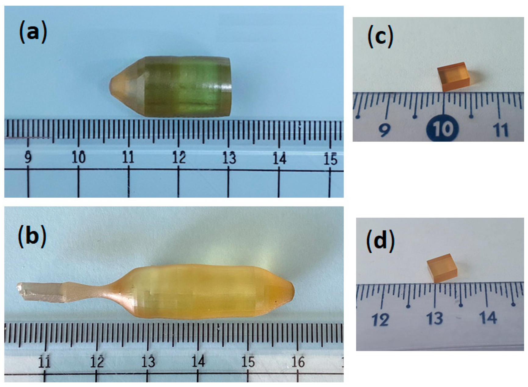
2.1. Crystal Growth

Active photonic devices, specifically waveguide lasers activated with rare earth ions from the lanthanide series, such as neodymium (Nd3+), praseodymium (Pr3+), holmium (Ho3+), or ytterbium (Yb3+), have been developed in the last years [13,14,15,16]. Among them, Nd3+ has significant importance for laser emission at 1 μm from waveguide lasers offering high optical gain and low lasing threshold. Yb3+ is competing with Nd3+ for laser emission in the 1 μm spectral region because it has a smaller quantum defect, thus the thermal load on the active medium is low and potentially allows for high-power laser generation with high slope efficiencies, broader emission bandwidth, and longer upper-laser level lifetime, enabling tunable laser emission or generation of ultrashort pulses.
In our case, the Nd:CLNGG and Yb:CLNGG crystals with Nd3+ and Yb3+ dopant ions concentrations of 0.7 at.% and 7.28 at.%, respectively, further denoted as 0.7-at.% Nd:CLNGG and 7.28-at.% Yb:CLNGG, were grown by the Czochralski method. The conventional solid-state reaction method was used to synthesize the corresponding polycrystalline Nd:CLNGG and Yb:CLNGG starting materials. CaCO3 (99.95% purity), Li2CO3 (99.998 purity), Nb2O5 (99.9985% purity), Ga2O3, Nd2O3, and Yb2O3 (of 5N purity) were used as raw materials. Considering that Nd3+ and Yb3+ dopant ions replace Ca2+ ions in the CLNGG host matrix and the values of the effective segregation coefficients (keff) of Nd3+ and Yb3+ in the CLNGG crystal are 0.55 [7] and 0.91 [17], respectively, the chemical compositions of the starting materials were established to be 1.28-at.% Nd:CLNGG and 8-at.% Yb:CLNGG, respectively. The raw materials were weighed according to the chemical equations:
3CaCO3 + 0.13926Li2CO3 + 0.88926Nb2O5 + 1.50348Ga2O3 + 0.0192Nd2O3
Ca3Li0.275Nb1.775Ga2.95O12·0.0128Nd3 Li0.275Nb0.275Ga4.45O12 + 3.13926CO2
3CaCO3 + 0.1485Li2CO3 + 0.8985Nb2O5 + 1.653Ga2O3 + 0.12Yb2O3
Ca3Li0.275Nb1.775Ga2.95O12·0.08Yb3 Li0.275Nb0.275Ga4.45O12 + 3.1485CO2
The materials were mixed by grounding in an agate mortar, pressed into cylindrical tablets, and sintered at 1300 °C for 24 h. The growth process was carried out in an air atmosphere using platinum crucibles with an internal diameter and a height of 30 mm. All crystals were grown on crystalline seeds oriented along the ⟨111⟩ direction cut from an undoped CLNGG crystal. The growth temperature was determined to be about 1450 ± 10 °C; the pulling and rotation rates were kept constant at 1 mm/h and 15 rpm, respectively, throughout the crystal growth processes. Finally, the as-grown crystals were annealed in an air atmosphere for 24 h at a temperature of 1300 °C to eliminate the residual thermal stress accumulated during growth, as well as to stabilize the trivalent oxidation state of the Nd and Yb dopant ions.

2.2. Experimental Setup for Laser Emission

An experimental set-up, described in our previous works [18,19], was used to characterize the emission performances of the laser crystals. For the Nd:CLNGG medium, the optical pumping was carried out with a fiber-coupled diode laser (LIMO Co., Dortmund, Germany) with emission at 807 nm (λp) wavelength, while the Yb:CLNGG crystal was pumped in the highly absorbing level at λp = 973 nm with a fiber-coupled diode laser (LIMO Co., Germany). In order to mitigate the thermal effects induced in the crystal when pumping in continuous wave (CW) mode, the two diode lasers will be operated in quasi-CW conditions (1 ms pump pulse duration, repetition rate of 5 Hz). A multimode fiber with diameter ϕ = 100 μm and numerical aperture NA = 0.22 was used to transfer the diode laser radiation in each laser medium, by imaging the beam with a focusing line containing two lenses, one of 50 mm focal length and one of 30 mm focal length.
In the setup, two plane parallel mirrors, dedicated for each crystal type, were placed very close to the lateral surfaces of the crystals and used as a linear resonator. In the case of Nd:CLNGG crystal, the resonator rear mirror was coated for high reflectivity HR (R > 0.998) at the emission wavelength (λem) of 1.06 μm and with high transmission HT (T > 0.98) at λp = 807 nm. For the Yb:CLNGG crystal, we have used a rear mirror with HR coating (R > 0.998) at λem = 1.03 μm and with HT (T > 0.98) at λp = 973 nm. Out-coupling mirrors (OCM) with various transmissions T at the laser wavelength, λem were used. The gain media were consecutively positioned on a metallic plate with no further cooling. A CMOS camera was used to visualize the output surfaces of the waveguides during optical pumping. The laser beam near-field distributions were recorded with a SP620U Spiricon camera (spectral range from 190 nm to 1100 nm).

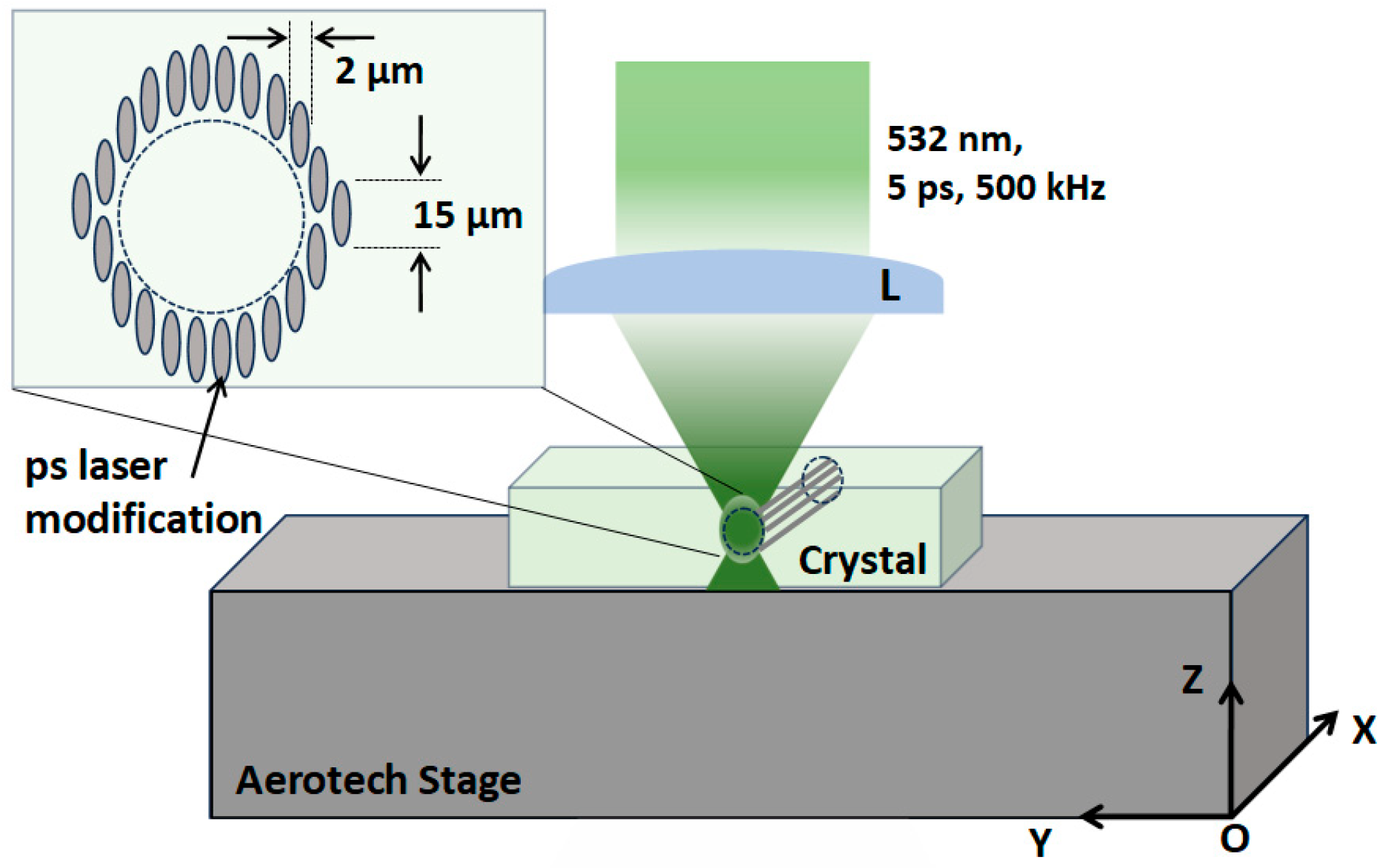
2.3. Waveguides Writing with Ps-Laser Pulses

The experimental set-up used for waveguides writing in the Nd:CLNGG and Yb:CLNGG crystals is represented schematically in Figure 1. The beam from a ps-laser system (from Lumera, Coherent, USA), delivering pulses at 532 nm wavelength with 5 ps duration and 100 μJ maximum energy at 500 kHz repetition rate, was focused 500 μm beneath the surface of the two media with an aspheric lens (L) of 6.24 mm focal length and NA = 0.40. The focal spot (measured in air) had a diameter of ~2.0 μm. The focusing position, on the surface and inside the media, was visualized and controlled with a CCD camera. The writing process was managed by placing the two media on an Aerotech PlanarDL motorized translation stage with computer control and ±500 nm resolution. The location of the beam on the Oz axis was adjusted by controlling the focusing lens position with an additional translation stage. Extensive preliminary tests were performed over a wide range of values for laser pulse energy, motorized scanning speed and tracks separation in order to obtain the optimal laser processing parameters. Based on these results, the waveguides were inscribed with pulse energy of 0.15 μJ at 1 mm/s scanning speed. The distance between the two consecutive tracks was set at 5 μm.

3. Results

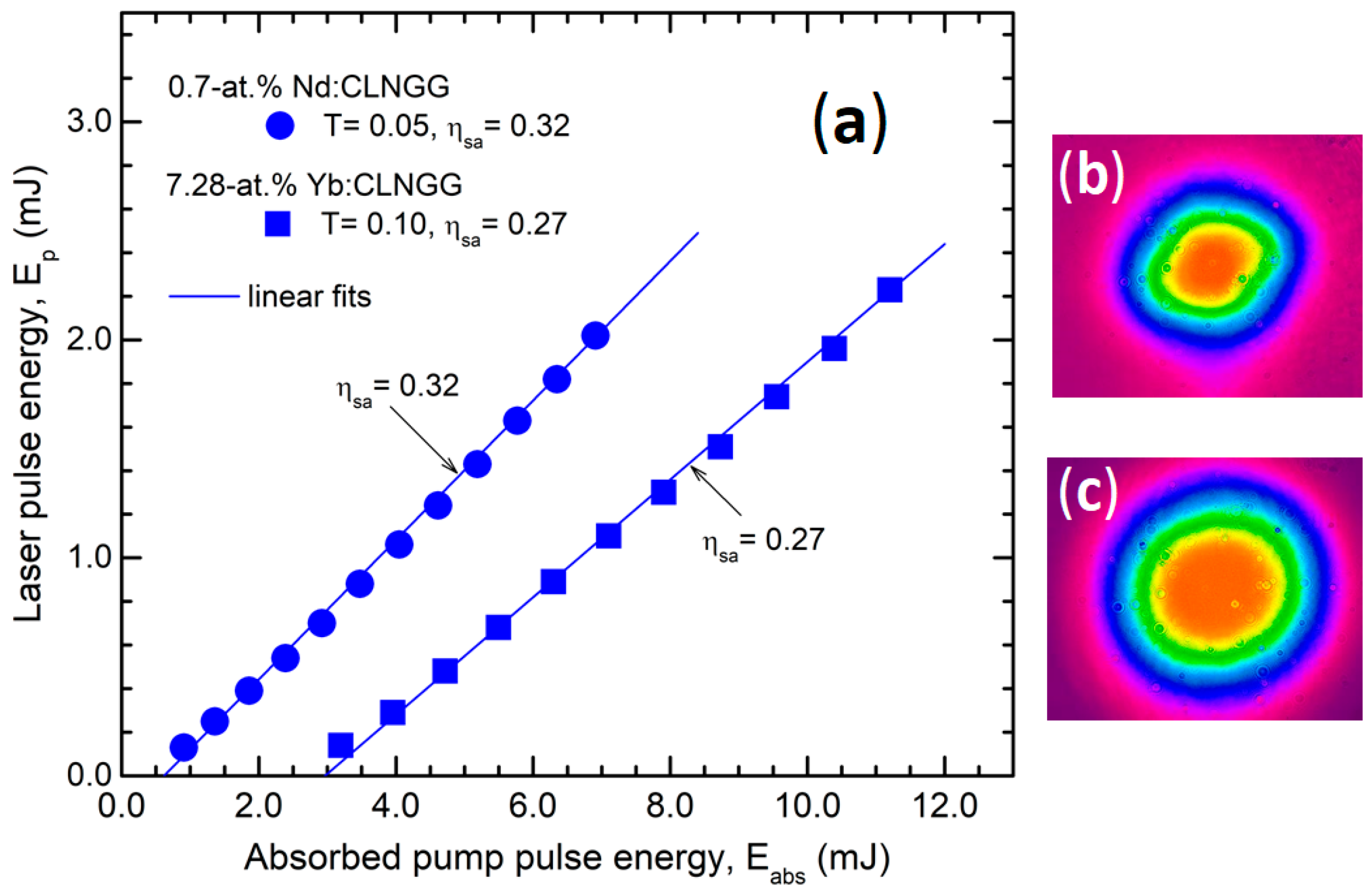
3.1. Characterization of Bulk Crystals

Each laser crystal was investigated by optical microscopy and prepared for further investigations, targeting the emission performances measurements and laser waveguides inscribing. A photo of the Nd:CLNGG crystal is shown in Figure 2a, while the as-grown Yb:CLNGG crystal is presented in Figure 2b. The crystals have no visible defects and no scattering centers under illumination with a He-Ne laser were observed. Several pieces, having 3.0 × 3.9 × 5.9 mm3 for Nd:CLNGG and 3.0 × 4.0 × 5.0 mm3 for Yb:CLNGG were cut from the grown crystals and polished to laser-grade quality for optical properties characterization and laser processing, as shown in Figure 2c,d, respectively.
Using the setup described above, we investigated the laser emission performances for bulk 0.7-at.% Nd:CLNGG at λem = 1.06 μm and for bulk 7.28-at.% Yb:CLNGG at λem = 1.03 μm, for quasi-CW pumping regime (Figure 3a). The near-field beam profiles are shown in Figure 3b for Nd:CLNGG and Figure 3c for Yb:CLNGG. For each laser crystal, the emission characteristics were determined, and the results are specified in Table 1.

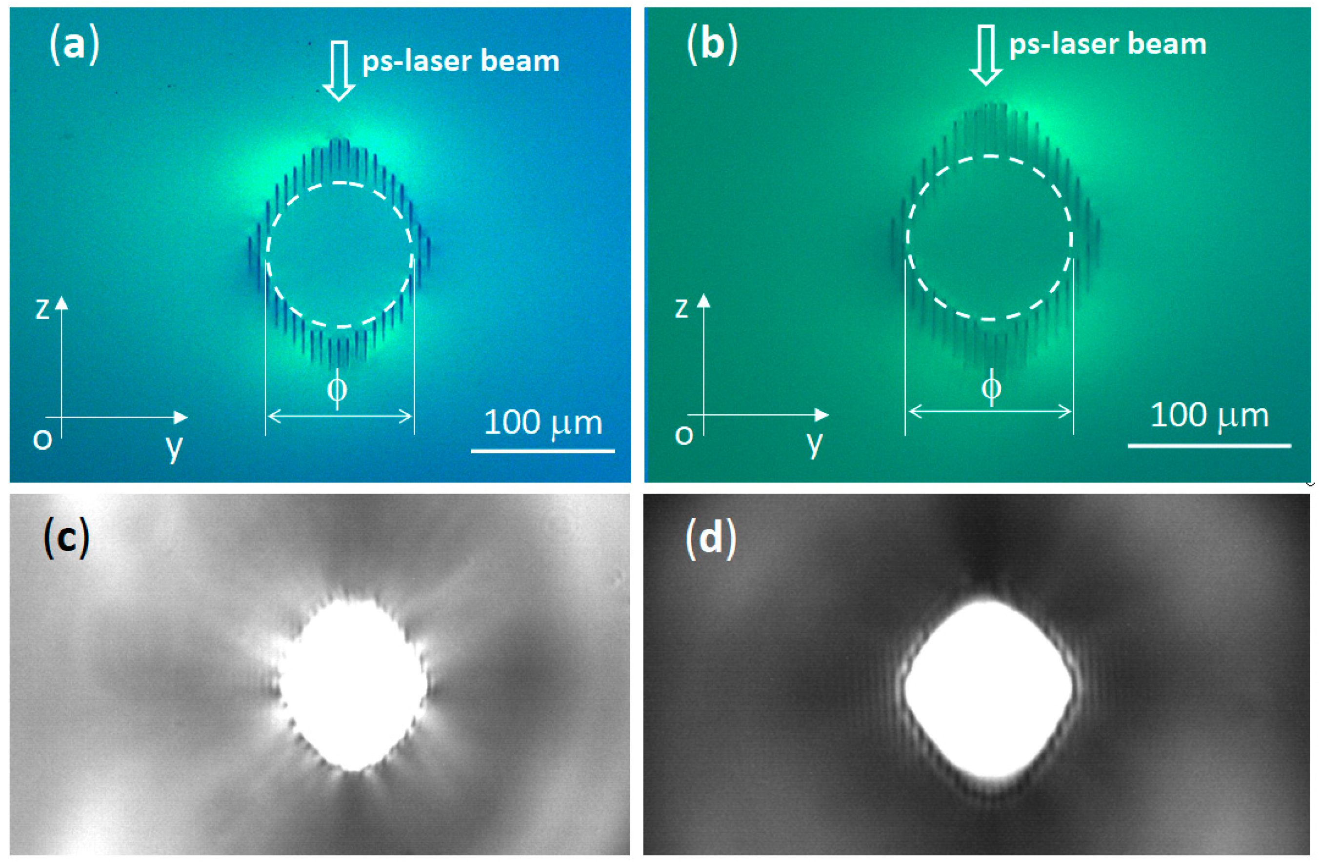
3.2. Waveguide Fabrication by Ps-Laser Irradiation

Buried depressed-cladding waveguide with circular shape and diameter ϕ = 100 μm were inscribed in Nd:CLNGG (denoted by NCLNGG-C) and Yb:CLNGG (denoted by YCLNGG-C) using the experimental setup described in Section 2.3. By inscribing parallel tracks on the Ox direction, with 1 mm/s scan speed, we have realized circular-shaped waveguides centered at 500 μm under the crystal’s surface. The 532 nm inscribing beam is translated on the crystal’s full length and the position along axis Oz is calculated and adjusted at each layer to generate a circular contour in the center. A microscope was used to record cross-section images of the waveguides, as shown in Figure 4a for NCLNGG-C and in Figure 4b for YCLNGG-C. After a qualitative evaluation, it was concluded that the tracks are smooth, and no cracks were observed. Tracks with similar sizes were inscribed in both crystals, using the same level of pulse energy of 0.15 μJ, indicating that the refractive index modification depends on the gain medium properties, on the laser exposure conditions and not on the rare-earth ion dopant. Images of the waveguide exit surfaces are illustrated in Figure 4c,d during the optical pumping; a low leakage is observed between the written tracks. Although the high repetition rate assures a reduced laser power fluctuation during the waveguide fabrication, controlling the track position overlap without inducing crystal damage remains a challenge. Nevertheless, we optimized the waveguide fabrication process by reducing the total number of tracks to 40, finishing the writing process in less than 6 min, a reduced value compared with other methods [18].
The level of propagation losses was determined for each waveguide. To do this, the beam from a HeNe laser (emission at 632.8 nm) was coupled (coupling efficiency close to unity) into each structure and the power of the transmitted light was measured. After subtracting the coupling and the Fresnel losses, the propagation losses were determined to be 0.9 dB/cm for the NCLNGG-C waveguide and 2.5 dB/cm for the YCLNGG-C waveguide, whereas for the bulk materials the corresponding losses were 0.4 dB/cm for Nd:CLNGG and 0.8 dB/cm for Yb:CLNGG. This loss level is below that obtained for buried depressed-cladding waveguides inscribed in the same crystals [20]: 2.6 dB/cm at 632.8 nm for an elliptical waveguide realized in 0.7-at.% Nd:CLNGG (5.9-mm length) and 5.6 dB/cm, for a waveguide with elliptical shape realized in a 4.3-at.% Yb:CLNGG crystal (length of 3.0 mm). The later waveguides were realized using an amplified laser system delivering pulses at 775 nm with 200 fs duration at 2 kHz repetition rate. We assume that the use of ps-laser pulses for waveguide fabrication in crystals with stronger nonlinear properties leads to the creation of a smaller number of lattice defects compared to waveguides realized with typical fs-laser systems leading to a lower level of propagation losses. We can observe that the loss level for Yb:CLNGG is higher and this may be due to the lower optical quality of this crystal. The interplay between laser pulse wavelength used for writing, pulse duration, and pulse repetition rate can contribute to the improvement of the waveguides optical properties. Also, we expect to further decrease the propagation losses by setting a lower value than 5 μm between the parallel tracks.

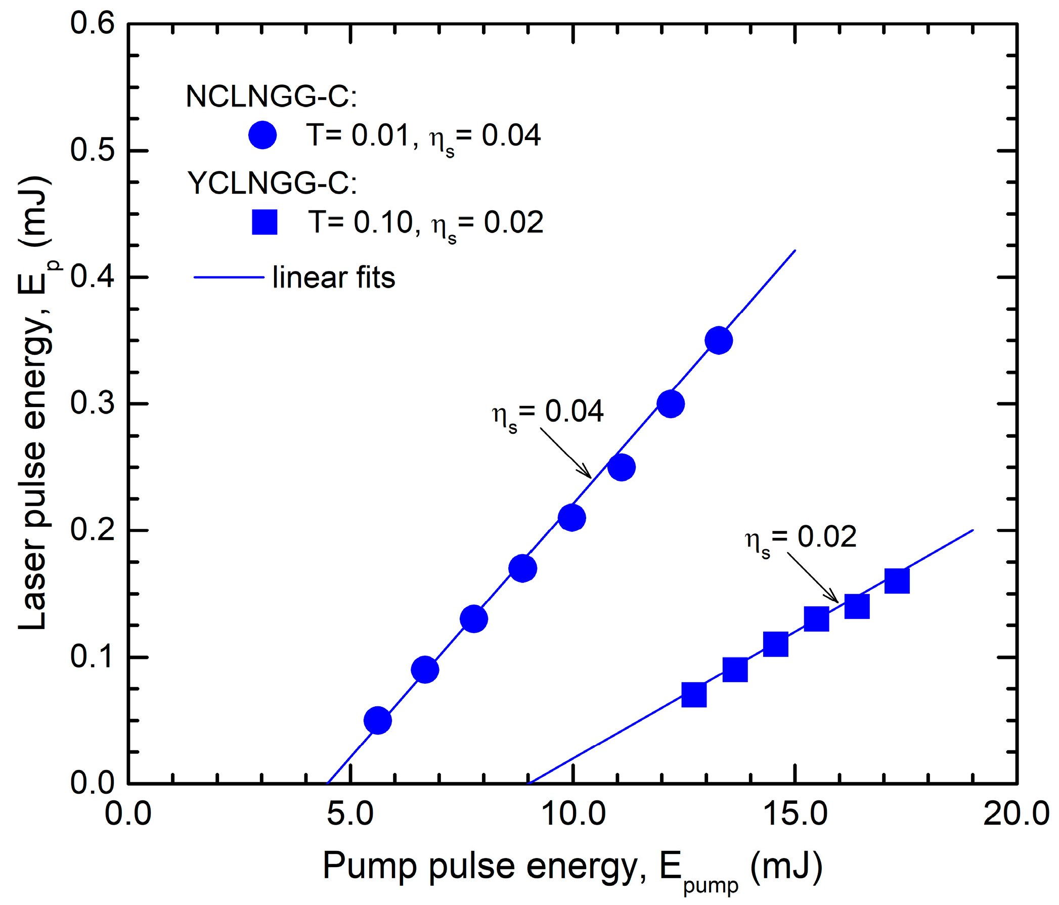
3.3. Laser Emission from Circular Waveguides

Laser emission was generated for the waveguides inscribed in the two gain media. A high coupling efficiency (close to one) of each pump beam into the corresponding waveguide was achieved by carefully adjusting the pump-beam focusing position inside each laser crystal. A maximum laser pulse energy of Ep = 0.35 mJ was determined from the NCLNGG-C waveguide for Epump = 13.3 mJ (the overall optical-to-optical efficiency was ηo~0.03); the laser operated with a slope efficiency ηs = 0.04 (Figure 5). The YCLNGG-C waveguide yielded laser pulses with maximum energy Ep = 0.16 mJ for Epump = 17.3 mJ (i.e., ηo~0.01) and ηs = 0.02. The laser beam profiles corresponding to each waveguide were highly multimode.

4. Discussion

In this report, we describe for the first time the usage of high repetition rate ps-laser for waveguide fabrication starting with the crystal grown and ending with waveguide characterization. The increased interest in such devices is largely due to the compact geometry of the waveguide structures, allowing for light confinement and propagation in an extremely small volume of micrometric (μm) scale and, in this way, achieving intensity levels considerably higher than those in bulk materials. By combining the properties of waveguide structures with those of active laser media, miniaturized laser sources of increased potential for integrated optics can be realized with important advantages in terms of high optical gain and implicitly low lasing threshold, better management of thermal effects, and, thus, compatibility with laser diodes for operation at high power levels or beam shaping.
Waveguides were inscribed in various crystalline media with both types of morphological changes: Type I for positive refractive index modification (Δn > 0) and Type II for negative refractive index modification (Δn < 0). Type I modification is specific to glasses and several crystals, like LiNbO3 [21], KTP [22], Nd:YCOB [23], BGO [24], LiTaO3 [25], or Nd:YAG [26]. With Type II refractive index change, waveguides are realized in crystalline as well as in ceramic media with different geometries, such as depressed-cladding waveguides in Nd:YAG [27], two-line configuration in Yb:YAG [28] or optical-lattice-like layout in Nd:YAP [29]. This approach is suitable for rare-earth doped crystals because the influence of the laser–matter interaction is minimal in the waveguide core, preserving the spectroscopic properties. Moreover, buried depressed-cladding waveguides are suited for optical pumping with fiber-coupled diode lasers with emission in the infrared region and for further power scaling. Regarding waveguide realization in disordered gallium garnet crystals, there are a couple of reports from Tan et al. on laser emission at different wavelengths from waveguides inscribed in Nd-doped CNGG crystal [30,31].
The use of ps-pulsed laser installations to realize waveguide structures generates 1.06 μm laser emission with output pulse energy Ep = 0.35 mJ and slope efficiency ηs = 0.04 for the circular waveguide with ϕ = 100 µm diameter realized in Nd:CLNGG and laser emission at the wavelength of 1.03 μm with output pulse energy Ep = 0.16 mJ and slope efficiency ηs = 0.02 for Yb:CLNGG. The value for ηs is comparable with the work conducted by Tan et al. [30]. The propagation losses at 632.8 nm were evaluated to be 0.9 dB/cm for the waveguide realized in the Nd:CLNGG and 2.5 dB/cm for the one inscribed in the Yb:CLNGG crystal. Table 2 summarizes the conditions used to inscribe buried depressed-cladding waveguides with large diameter in different active media, using fs- and ps-laser pulses. The propagation losses are also indicated, these being measured by coupling in the waveguides a HeNe laser beam at 632.8 nm. It can be seen that, in general, the losses are similar, but writing with ps-laser pulses was performed at a higher repetition rate than that with fs-laser pulses, which ensured a faster inscribing speed.
Although we have used the same laser exposure conditions, the losses between the two crystals may be due to factors such as the crystal’s lower optical quality or even the refractive index modification realized by the ps laser. On the other hand, propagation losses could be reduced by inscribing depressed-cladding waveguides with an “ear-like” structure. This configuration, recently proposed, allowed efficient laser emission in Nd:YAG [38] or Pr:YLF [39]. The physical processes initiated during crystal irradiation by the high repetition rate ps laser are still under debate, and most of the time the fs model is used, which is based on nonlinear photoionization processes. In this case, the excited carriers will linearly absorb photons and subsequently impact ionized bound electrons, thus generating an electron avalanche. Then, the accumulated energy is transferred to the irradiated material through electron-photon scattering on a ps time scale and carried out via thermal diffusion, finally inducing moderately strong refractive index modifications in the range of Δn = 10−4 to 10−2 [40,41]. For sub-ps laser pulses, the nonlinear absorption phenomena take place on a shorter scale than the electron–phonon scattering time and, in this way, heat diffusion outside the focal area is minimized.
For longer pulse duration, as is the situation with pulses ranging from 1 to 10 ps, the nonlinear photo-ionization processes occur on the same time scale as the energy transfer process to the lattice via phonon scattering; consequently, a heat accumulation effect appears. This effect may be deleterious regarding the optical properties of the waveguide structures. However, the interplay of other laser parameters such as laser pulse energy, repetition rate, and scan speed, whose values show significant importance in the optimization process of these properties, has the capability to reduce the negative impact of longer pulse durations. This interplay of laser parameters allows the usage of both fs- and ps-laser systems delivering pulses at low to moderate (1–200 kHz) and, also, at high repetition rates (>200 kHz). At high repetition rates, heat builds up around the irradiated volume because the time between the laser pulses is shorter than the time for the accumulated energy to diffuse out of the volume. It has been reported that waveguides written in this regime have superior optical properties (in terms of mode symmetry and lower propagation losses) than those inscribed in the low repetition rate regime due to the presence of a rapid annealing effect. These improved results have been successfully explained in terms of a partial recombination of defects for waveguides realized in Yb:YAG ceramic laser gain medium [42].

5. Conclusions

Buried depressed-cladding waveguides with circular geometry have been realized in 0.7-at.% Nd:CLNGG and 7.28-at.% Yb:CLNGG disordered crystals by ps-laser beam exposure, for the first time to our best knowledge. The laser emission performances at 1.06 μm and 1.03 μm were evaluated under the pump at 807 nm (for Nd:CLNGG) and at 973 nm (for Yb:CLNGG) with a fiber-coupled diode lasers. Circular cladding waveguides of 100 μm diameter realized in Nd:CLNGG and Yb:CLNGG crystals delivered laser pulses at 1.06 μm with 0.35 mJ output energy, respectively, at 1.03 μm with 0.16 mJ output energy. The slope efficiencies were 0.04 and 0.02 for the two waveguides, respectively. The waveguide realized in RE3+-doped CLNGG crystals using ps-laser pulses at high repetition rates could provide miniaturized pulsed laser sources (Q-switched or mode-locked) by further integrating a suitable saturable absorber. The direct laser writing technique was used to inscribe waveguides in these crystals and proved once again its ability to induce refractive index modifications in a multitude of dielectric materials, even if the laser – matter interaction is a rather complex process and the phenomena as well as the structural effects are not completely understood. The growth by the Czochralski technique of Nd- and Yb-doped CLNGG disordered laser crystals with superior optical quality is among our current research priorities. These new crystals will allow inscribing buried depressed-cladding waveguides with different sizes, as well as scaling of laser emission using the pump with fiber-coupled diode lasers.

Author Contributions

Conceptualization, G.C.; formal analysis, G.C., F.J., M.G., A.B., F.V., L.G., and N.P.; funding acquisition, G.C.; investigation, G.C., F.J., M.G., A.B., F.V., and L.G.; methodology, G.C., F.J., and N.P.; supervision, N.P.; validation, G.C. and F.J.; visualization: G.C.; writing—original draft preparation, G.C., F.J., L.G., and N.P.; writing—review and editing, G.C., F.J., L.G., and N.P. All authors have read and agreed to the published version of the manuscript.

Funding

This work was financed by project PD63/2022, PN-III-P1-1.1-PD-2021-0522 and project PCE30/2022 PN-III-P4-PCE-2021-0519, CNCS-UEFISCDI, both within PNCDI III, and partially supported by program NUCLEU-LAPLAS VII/30N/2023, Ministry of Research, Education and Digitization, Romania.

Institutional Review Board Statement

Not applicable.

Informed Consent Statement

Not applicable.

Data Availability Statement

Data underlying the results presented in this paper may be obtained from the authors upon reasonable request.

Acknowledgments

The support of National Interest Infrastructure facility IOSIN-CETAL at the National Institute for Laser, Plasma and Radiation Physics is acknowledged.

Conflicts of Interest

The authors declare no conflicts of interest.

References

  1. Corbari, C.; Champion, A.; Gecevičius, M.; Beresna, M.; Bellouard., Y.; Kazansky, P.G. Femtosecond versus picosecond laser machining of nano-gratings and micro-channels in silica glass. Opt. Express 2013, 21, 3946–3958. [Google Scholar] [CrossRef] [PubMed]
  2. Zhang, H.; Eaton, S.M.; Herman, P.R. Low-loss Type II waveguide writing in fused silica with single picosecond laser pulses. Opt. Express 2006, 14, 4826–4834. [Google Scholar] [CrossRef] [PubMed]
  3. McMillen, B.; Zhang, B.; Chen, K.P.; Benayas, A.; Jaque, D. Ultrafast laser fabrication of low-loss waveguides in chalcogenide glass with 0.65 dB/cm loss. Opt. Lett. 2012, 37, 1418–1420. [Google Scholar] [CrossRef] [PubMed]
  4. Grivas, C.; Corbari, C.; Brambilla, G.; Lagoudakis, P.G. Tunable, continuous-wave Ti:sapphire channel waveguide lasers written by femtosecond and picosecond laser pulses. Opt. Lett. 2012, 37, 4630–4632. [Google Scholar] [CrossRef]
  5. Matthäus, G.; Kämmer, H.; Lammers, K.A.; Vetter, C.; Watanabe, W.; Nolte, S. Inscription of silicon waveguides using picosecond pulses. Opt. Express 2018, 26, 24089–24097. [Google Scholar] [CrossRef] [PubMed]
  6. Voron’ko, Y.K.; Gessen, S.B.; Es’kov, N.A.; Sobol’, A.A.; Ushakov, S.N.; Tsymbal, L.I. Efficient active media based on Nd3+-activated calcium niobium gallium garnets. Sov. J. Quantum Electron. 1990, 20, 246–249. [Google Scholar] [CrossRef]
  7. Shi, Z.B.; Zhang, H.J.; Wang, J.Y.; Yu, Y.G.; Wang, Z.P.; Yu, H.H.; Sun, S.Q.; Xia, H.R.; Jiang, M.H. Growth and characterization of Nd:CLNGG crystal. J. Cryst. Growth 2009, 311, 3792–3796. [Google Scholar] [CrossRef]
  8. Yuxian, S.; Li, Q.; Zhang, D.; Feng, B.; Zhang, Z.; Zhang, H.; Wang, J. Comparison of 885 nm pumping and 808 nm pumping in Nd:CNGG laser operating at 1061 nm and 935 nm. Opt. Commun. 2010, 283, 2888–2891. [Google Scholar] [CrossRef]
  9. Lupei, V.; Lupei, A.; Gheorghe, C.; Gheorghe, L.; Achim, A.; Ikesue, A. Crystal field disorder effects in the optical spectra of Nd3+ and Yb3+-doped CLNGG laser crystals and ceramics. J. Appl. Phys. 2012, 112, 063110. [Google Scholar] [CrossRef]
  10. Yu, H.; Zhang, H.; Wang, Z.; Wang, J.; Yu, Y.; Shi, Z.; Zhang, X.; Jiang, M. Continuous-wave and passively Q-switched laser performance with a disordered Nd:CLNGG crystal. Opt. Express 2009, 17, 19015–19020. [Google Scholar] [CrossRef] [PubMed]
  11. Lin, Z.L.; Loiko, P.; Zeng, H.J.; Xue, W.Z.; Zhang, G.; Normani, S.; Camy, P.; Petrov, V.; Mateos, X.; Lin, H.; et al. Kerr-lens mode-locking of an Yb:CLNGG laser. Opt. Express 2023, 31, 8575–8585. [Google Scholar] [CrossRef] [PubMed]
  12. Adair, R.; Chase, L.L.; Payne, A. Nonlinear refractive index of optical crystals. Phys. Rev. B 1989, 39, 3337–3350. [Google Scholar] [CrossRef] [PubMed]
  13. Li, L.; Kong, W.; Chen, F. Femtosecond laser-inscribed optical waveguides in dielectric crystals: A concise review and recent advances. Adv. Photon. 2022, 4, 024002. [Google Scholar] [CrossRef]
  14. Shen, Y.; Jia, Y.; Chen, F. Femtosecond laser-induced optical waveguides in crystalline garnets: Fabrication and application. Opt. Laser Technol. 2023, 164, 109528. [Google Scholar] [CrossRef]
  15. Baiocco, D.; Lopez-Quintas, I.; Vazquez de Aldana, J.R.; Tonelli, M.; Tredicucci, A. Diode-pumped visible lasing in femtosecond-laser-written Pr:LiLuF4 waveguide. Opt. Lett. 2023, 48, 1734–1737. [Google Scholar] [CrossRef] [PubMed]
  16. McDaniel, S.A.; Berrya, P.A.; Cooka, G.; Zelmona, D.; Meissnerc, S.; Meissnerc, H.; Muc, X. CW and passively Q-Switched operation of a Ho:YAG waveguide laser. Opt. Laser Technol. 2017, 91, 1–6. [Google Scholar] [CrossRef]
  17. Alvarez-Perez, J.O.; Cano-Torres, J.M.; Ruiz, A.; Serrano, M.D.; Cascales, C.; Zaldo, C. A roadmap for laser optimization of Yb:Ca3(NbGa)5O12-CNGG-type single crystal garnets. J. Mater. Chem. C 2021, 9, 4628. [Google Scholar] [CrossRef]
  18. Salamu, G.; Jipa, F.; Zamfirescu, M.; Pavel, N. Laser emission from diode-pumped Nd:YAG ceramic waveguide lasers realized by direct femtosecond-laser writing technique. Opt. Express 2014, 22, 5177–5182. [Google Scholar] [CrossRef] [PubMed]
  19. Salamu, G.; Jipa, F.; Zamfirescu, M.; Pavel, N. Cladding waveguides realized in Nd:YAG ceramic by direct femtosecond-laser writing with a helical movement technique. Opt. Mater. Express 2014, 4, 790–797. [Google Scholar] [CrossRef]
  20. Croitoru, G.; Anghel, I.; Voicu, F.M.; Greculeasa, M.; Broasca, A.; Gheorghe, L.M.; Pavel, N. Buried Depressed-Cladding Waveguides Fabricated in RE3+:CLNGG Laser Crystals using Direct Laser Writing Technique. In Proceedings of the Lasers and Electro-Optics/Europe-European Quantum Electronics Conferences (CLEO®/Europe-EQEC 2023), Munich, Germany, 26–30 June 2023. [Google Scholar] [CrossRef]
  21. Burghoff, J.; Nolte, S.; Tunnermann, A. Origins of waveguiding in femtosecond laser-structured LiNbO3. Appl. Phys. A 2007, 89, 127–132. [Google Scholar] [CrossRef]
  22. Campbell, S.; Thomson, R.R.; Hand, D.P.; Kar, A.K.; Reid, D.T.; Canalias, C.; Pasiskevicius, V.; Laurell, F. Frequency-doubling in femtosecond laser inscribed periodically-poled potassium titanyl phosphate waveguides. Opt. Express 2007, 15, 17146–17150. [Google Scholar] [CrossRef] [PubMed]
  23. Rodenas, A.; Kar, A.K. High-contrast step-index waveguides in borate nonlinear laser crystals by 3D laser writing. Opt. Express 2011, 19, 17820–17833. [Google Scholar] [CrossRef] [PubMed]
  24. He, R.; Hernández-Palmero, I.; Romero, C.; Vázquez de Aldana, J.R.; Chen, F. Three-dimensional dielectric crystalline waveguide beam splitters in mid-infrared band by direct femtosecond laser writing. Opt. Express 2014, 22, 31293–31298. [Google Scholar] [CrossRef] [PubMed]
  25. Wu, B.; Zhang, B.; Liu, W.; Lu, Q.; Wang, L.; Chen, F. Recoverable and rewritable waveguide beam splitters fabricated by tailored femtosecond laser writing of lithium tantalate crystal. Opt. Laser Technol. 2022, 145, 107500. [Google Scholar] [CrossRef]
  26. Zhang, Y.; Wu, J.; Wang, L.; Chen, F. Femtosecond laser direct writing of Nd:YAG waveguide with Type I modification: Positive refractive index change in track. Opt. Mat. 2021, 113, 110844. [Google Scholar] [CrossRef]
  27. Okhrimchuk, A.G.; Shestakov, A.V.; Khrushchev, I.; Mitchell, J. Depressed cladding, buried waveguide laser formed in a YAG:Nd3+ crystal by femtosecond laser writing. Opt. Lett. 2005, 30, 2248–2250. [Google Scholar] [CrossRef]
  28. Siebenmorgen, J.; Calmano, T.; Petermann, K.; Huber, G. Highly efficient Yb:YAG channel waveguide laser written with a femtosecond-laser. Opt. Express 2010, 18, 16035–16041. [Google Scholar] [CrossRef] [PubMed]
  29. Nie, W.; He, R.; Cheng, C.; Rocha, U.; Vázquez de Aldana, J.R.; Jaque, D.; Chen, F. Optical lattice-like cladding waveguides by direct laser writing: Fabrication, luminescence, and lasing. Opt. Lett. 2016, 41, 2169–2172. [Google Scholar] [CrossRef]
  30. Tan, Y.; Chen, F.; Vázquez de Aldana, J.R.; Yu, H.; Zhang, H. Tri-wavelength laser generation based on neodymium doped disordered crystal waveguide. Opt. Express 2013, 21, 22263. [Google Scholar] [CrossRef] [PubMed]
  31. Tan, Y.; Chen, F.; Vázquez de Aldana, J.R.; Yu, H.; Zhang, H. Quasi-three-level laser emissions of neodymium doped disordered crystal waveguides. IEEE J. Sel. Top. Quant. 2014, 21, 1601905. [Google Scholar] [CrossRef]
  32. Okhrimchuk, A.; Mezentsev, V.; Shestakov, A.; Bennion, I. Low loss depressed cladding waveguide inscribed in YAG:Nd single crystal by femtosecond laser pulses. Opt. Express 2012, 20, 3832–3843. [Google Scholar] [CrossRef] [PubMed]
  33. Liu, H.; Jia, Y.; Vázquez de Aldana, J.R.; Jaque, D.; Chen, F. Femtosecond laser inscribed cladding waveguides in Nd:YAG ceramics: Fabrication, fluorescence imaging and laser performance. Opt. Express 2012, 20, 18620–18629. [Google Scholar] [CrossRef] [PubMed]
  34. Liu, H.; Jia, Y.; Chen, F.; Vázquez de Aldana, J.R. Continuous wave laser operation in Nd:GGG depressed tubular cladding waveguides produced by inscription of femtosecond laser pulses. Opt. Express 2013, 3, 278–283. [Google Scholar] [CrossRef]
  35. Liu, H.; Tan, Y.; Vázquez de Aldana, J.R.; Chen, F. Efficient laser emission from cladding waveguide inscribed in Nd:GdVO4 crystal by direct femtosecond laser writing. Opt. Lett. 2014, 39, 4553–4556. [Google Scholar] [CrossRef] [PubMed]
  36. Pavel, N.; Salamu, G.; Jipa, F.; Zamfirescu, M. Diode-laser pumping into the emitting level for efficient lasing of depressed cladding waveguides realized in Nd:YVO4 by the direct femtosecond-laser writing technique. Opt. Express 2014, 22, 23057–23065. [Google Scholar] [CrossRef]
  37. Croitoru, G.; Jipa, F.; Pavel, N. Laser emission from buried depressed-cladding waveguides inscribed in Nd:YAG ceramics by picosecond-laser beam writing. Opt. Mater. 2024, 148, 114772. [Google Scholar] [CrossRef]
  38. Sun, X.; Sun, S.; Romero, C.; Vázquez de Aldana, J.R.; Liu, F.; Jia, Y.; Chen, F. Femtosecond laser direct writing of depressed cladding waveguides in Nd:YAG with “ear-like” structures: Fabrication and laser generation. Opt. Express 2021, 29, 4296–4307. [Google Scholar] [CrossRef] [PubMed]
  39. Baillard, A.; Loiko, P.; Romero, C.; Arroyo, V.; Vázquez de Aldana, J.R.; Fromager, M.; Benayad, A.; Braud, A.; Camy, P.; Mateos, X. Orange surface waveguide laser in Pr:LiYF4 produced by a femtosecond laser writing. Opt. Lett. 2023, 48, 6212–6215. [Google Scholar] [CrossRef] [PubMed]
  40. Gattass, R.; Mazur, E. Femtosecond laser micromachining in transparent materials. Nat. Photon. 2007, 2, 219–225. [Google Scholar] [CrossRef]
  41. Eaton, S.M.; Cerullo, G.; Osellame, R. Fundamentals of Femtosecond Laser Modification of Bulk Dielectrics. In Femtosecond Laser Micromachining; Osellame, R., Cerullo, G., Ramponi, R., Eds.; Topics in Applied Physics; Springer: Berlin/Heidelberg, Germany, 2012; Volume 123, pp. 3–18. [Google Scholar] [CrossRef]
  42. Benayas, A.; Silva, W.F.; Ródenas, A.; Jacinto, C.; Vázquez de Aldana, J.R.; Chen, F.; Tan, T.; Thomsom, R.R.; Psaila, N.D.; Reid, D.T.; et al. Ultrafast laser writing of optical waveguides in ceramic Yb:YAG: A study of thermal and non-thermal regimes. Appl. Phys. A. 2011, 104, 301–309. [Google Scholar] [CrossRef]
Figure 1. The experimental set-up used for waveguide writing in the 0.7-at.% Nd:CLNGG and 7.28-at.% Yb:CLNGG ceramic is presented. L: lens.
Materials 17 01758 g001
Figure 2. The crystal boules after growing and annealing treatment: (a) 0.7-at.% Nd:CLNGG; (b) 7.28-at.% Yb:CLNGG. (c) Nd:CLNGG sample with 5.9-mm thickness; (d) Yb:CLNGG sample with 5.0-mm thickness.
Materials 17 01758 g002
Figure 3. (a) The laser pulse energy, Ep versus absorbed pump pulse energy, Eabs, for bulk Nd:CLNGG (OCM with T = 0.05 at λem = 1.06 μm) and bulk Yb:CLNGG (OCM with T = 0.10 at λem = 1.03 μm). The laser beam profile is shown for laser emission at maximum pump level in (b) Nd:CLNGG and (c) Yb:CLNGG.
Materials 17 01758 g003
Figure 4. Cross-section view for (a) waveguide NCLNGG-C and (b) waveguide YCLNGG-C; each waveguide boundary is marked by white dashed line. The exit side under optical pumping is presented for (c) waveguide NCLNGG-C and (d) waveguide YCLNGG-C.
Materials 17 01758 g004
Figure 5. The laser pulse energy, Ep versus pump pulse energy, Epump, for NCLNGG-C (OCM with T = 0.01 at λem = 1.06 μm) and YCLNGG-C (OCM with T = 0.10 at λem = 1.03 μm).
Materials 17 01758 g005
Table 1. Characteristics of laser emission at 1.06 μm from bulk 0.7-at.% Nd:CLNGG (OCM with T = 0.05) and at 1.03 μm from bulk 7.28-at.% Yb:CLNGG (OCM with T = 0.10).
Laser CrystalAbsorbed Pump Pulse Energy,
Eabs (mJ)
Absorption Efficiency,
ηa
Laser Pulse Energy,
Ep (mJ)
Optical Efficiency,
ηoa
Slope Efficiency,
ηsa
0.7-at.% Nd:CLNGG6.900.522.00.290.32
7.28-at.% Yb:CLNGG11.200.882.200.270.27
Table 2. A comparison of propagation losses for buried depressed-cladding waveguides with large diameter that were inscribed by linear translation technique [27] in different laser media is presented. The losses were determined at 632.8 nm with a HeNe laser. λ: laser beam wavelength; tp: laser pulse duration; Ep: pulse energy; f: repetition rate.
Laser CrystalWaveguide Diameter, ϕ (μm)Propagation Loss (dB/cm)Characteristics of the Writing BeamRef.
BulkWaveguideλ (nm)tpEp (μJ)f (kHz)Writing Speed
Nd:YAG crystalelliptical
116 μm × 110 μm
-0.12800110 fs1.2–1.51.00.5–0.7 mm/s[32] *
Nd:YAG ceramic~100-0.8800120 fs0.2–0.41.0700 μm/s[33]
Nd:GGG crystal90
120
150
-2.5
2.0
1.7
795120 fs2.11.0500 μm/s[34]
Nd:GdVO4150 0.7795120 fs1.681.0500 μm/s[35]
Nd:YVO4100-1.5–2.4775200 fs0.31.050 μm/s[36]
Nd:YAG ceramic50
100
0.21.0–1.2
1.5–1.8
775200 fs12.050 μm/s[18]
Nd:YAG ceramic1000.30.95325 ps0.25001 mm/s[37]
Nd:CLNGG
Yb:CLNGG
1000.4
0.8
0.9
2.5
5325 ps0.155001 mm/sthis work
* In this work, the propagation loss was determined from the threshold of laser emission.
Disclaimer/Publisher’s Note: The statements, opinions and data contained in all publications are solely those of the individual author(s) and contributor(s) and not of MDPI and/or the editor(s). MDPI and/or the editor(s) disclaim responsibility for any injury to people or property resulting from any ideas, methods, instructions or products referred to in the content.

