
A Review of β-Ga2O3 Power Diodes

Abstract
1. Introduction
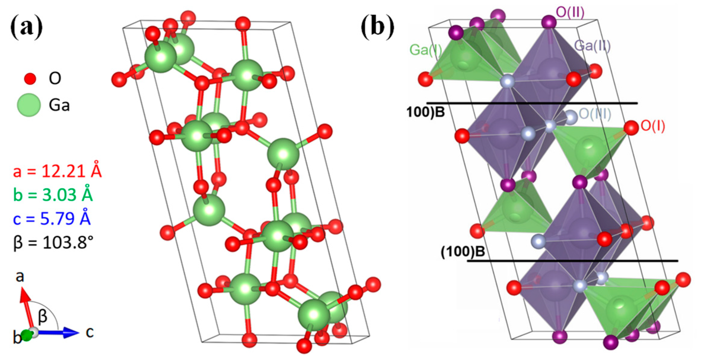
2. β-Ga2O3 Materials
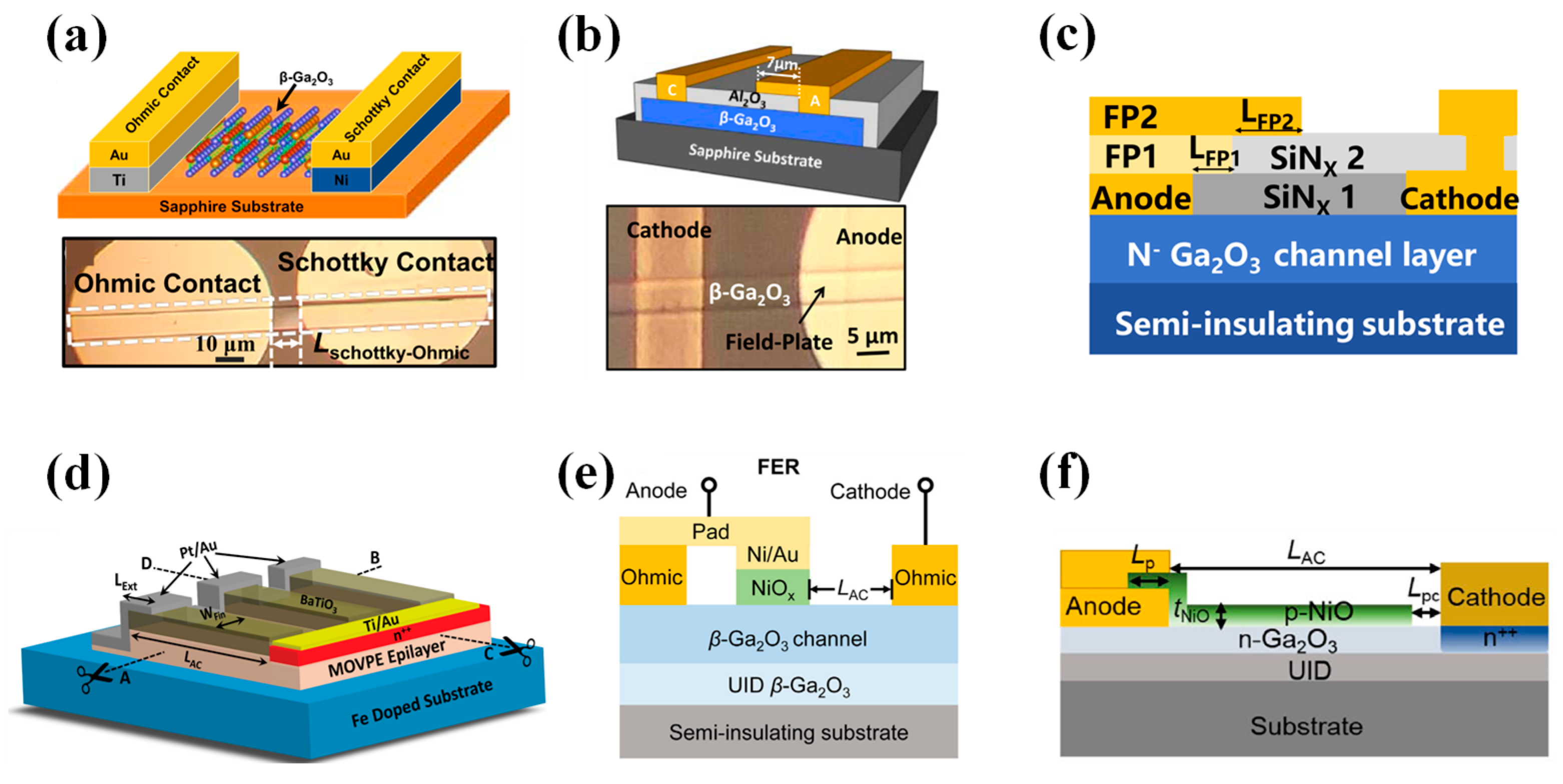
3. Metal/β-Ga2O3 Contact
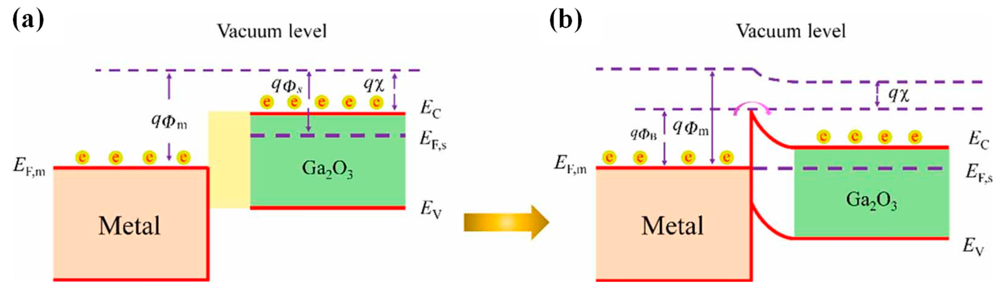
3.1. Schottky Contact
3.2. Ohmic Contact
4. β-Ga2O3 Power Diodes
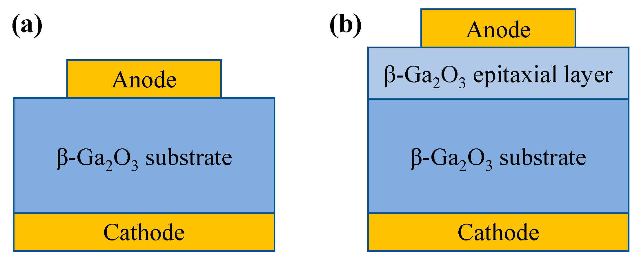
4.1. Vertical-Structure SBDs
4.1.1. Simple Structure
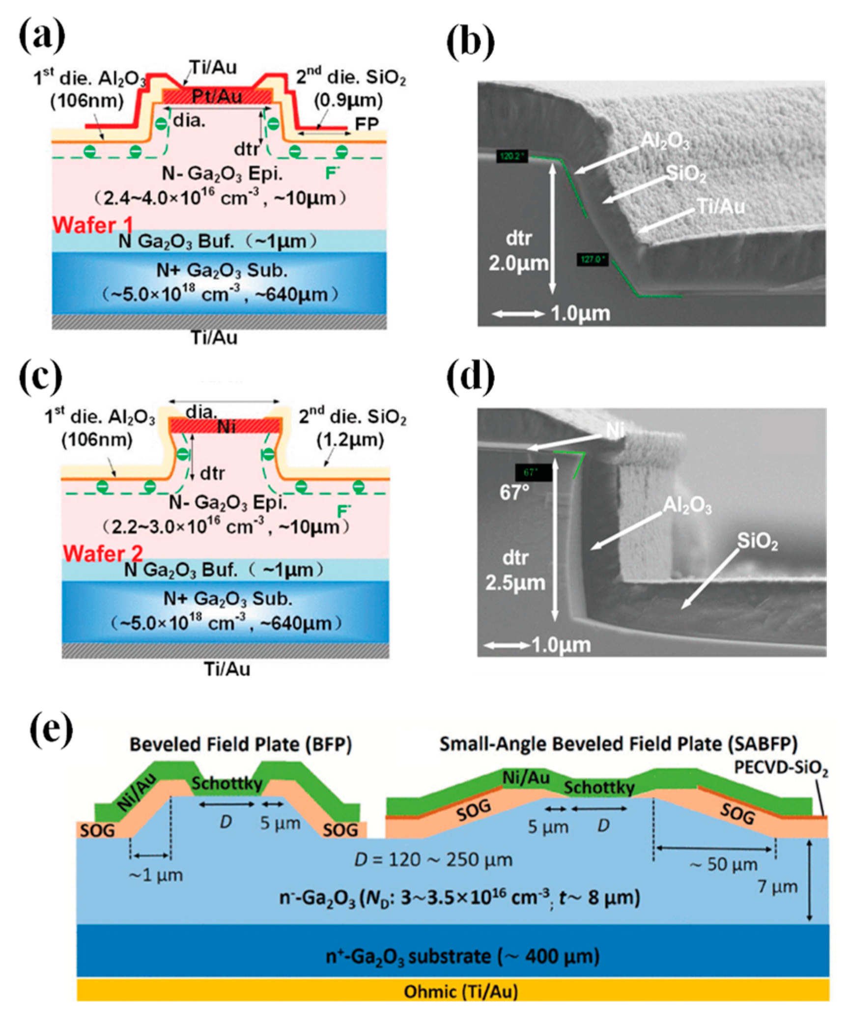
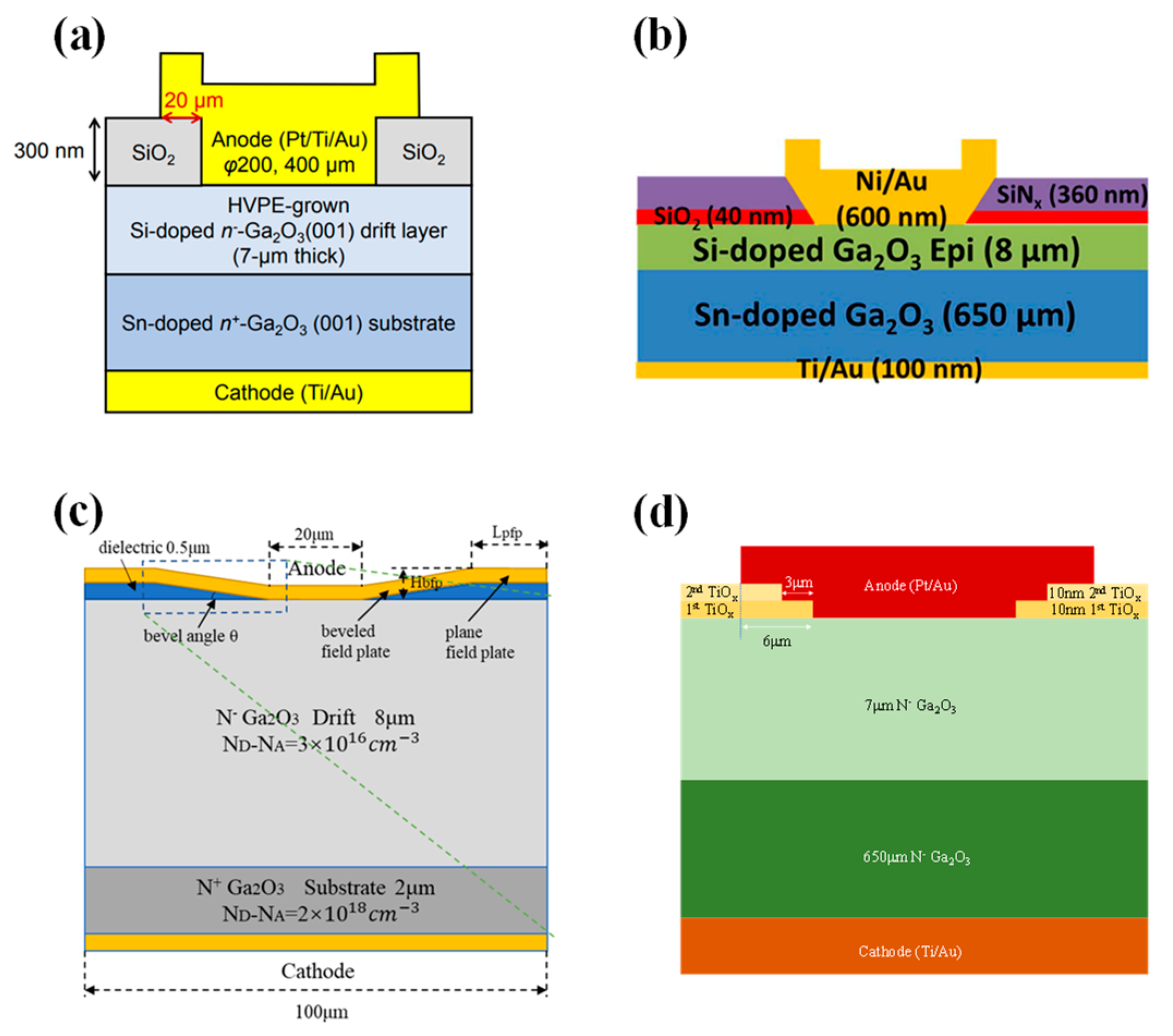
4.1.2. Field Plate Structure
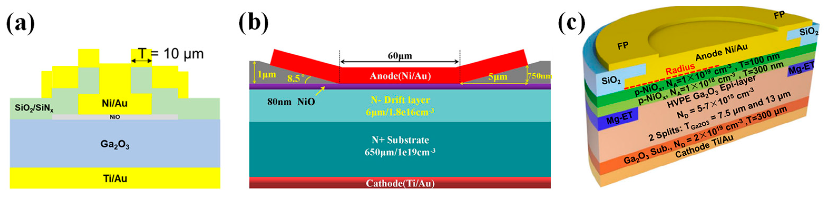
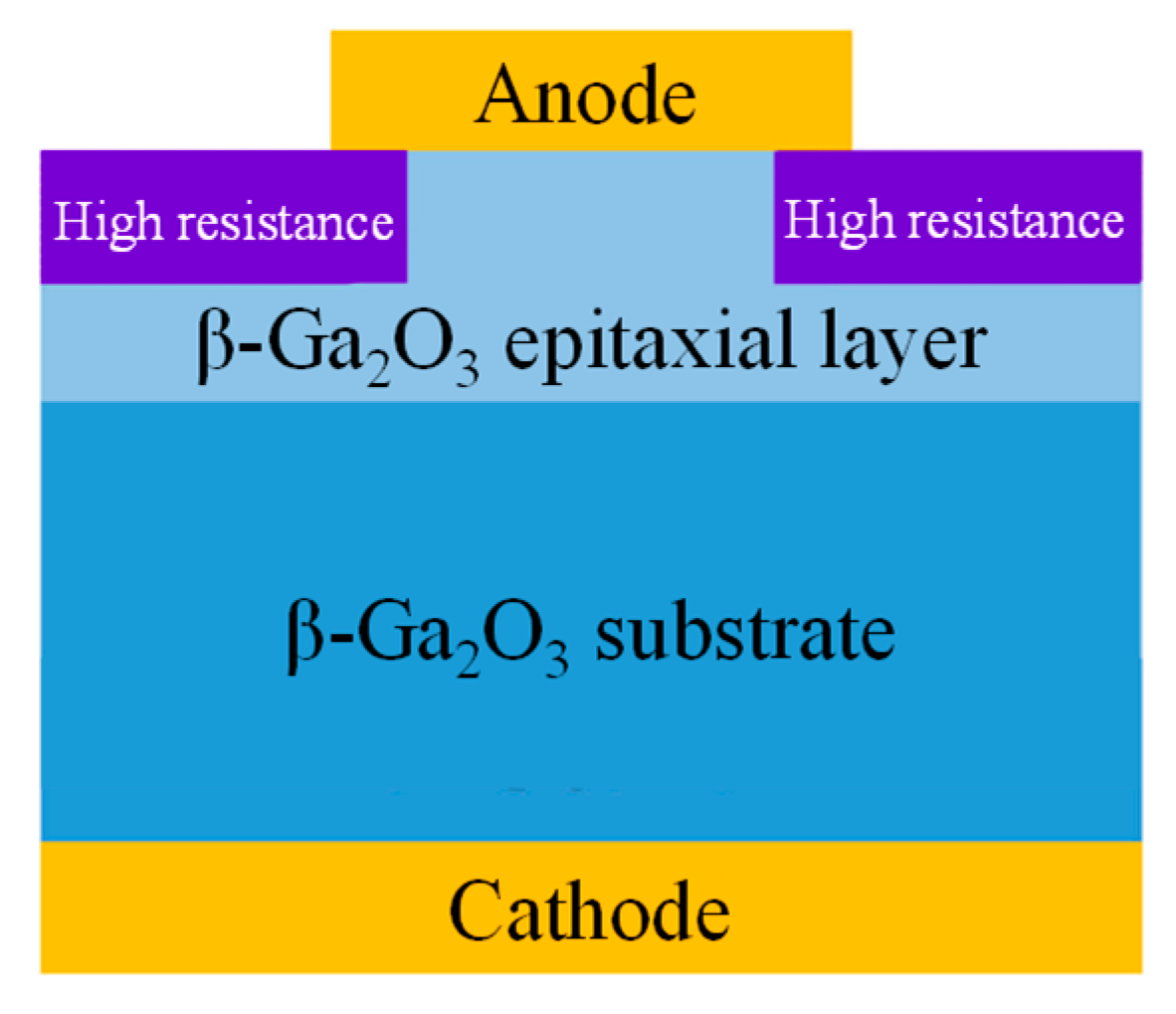
4.1.3. Edge Termination Structure
4.1.4. Trench Structure

4.1.5. Mesa Termination Structure
4.2. Vertical Heterojunction-Structure Diodes
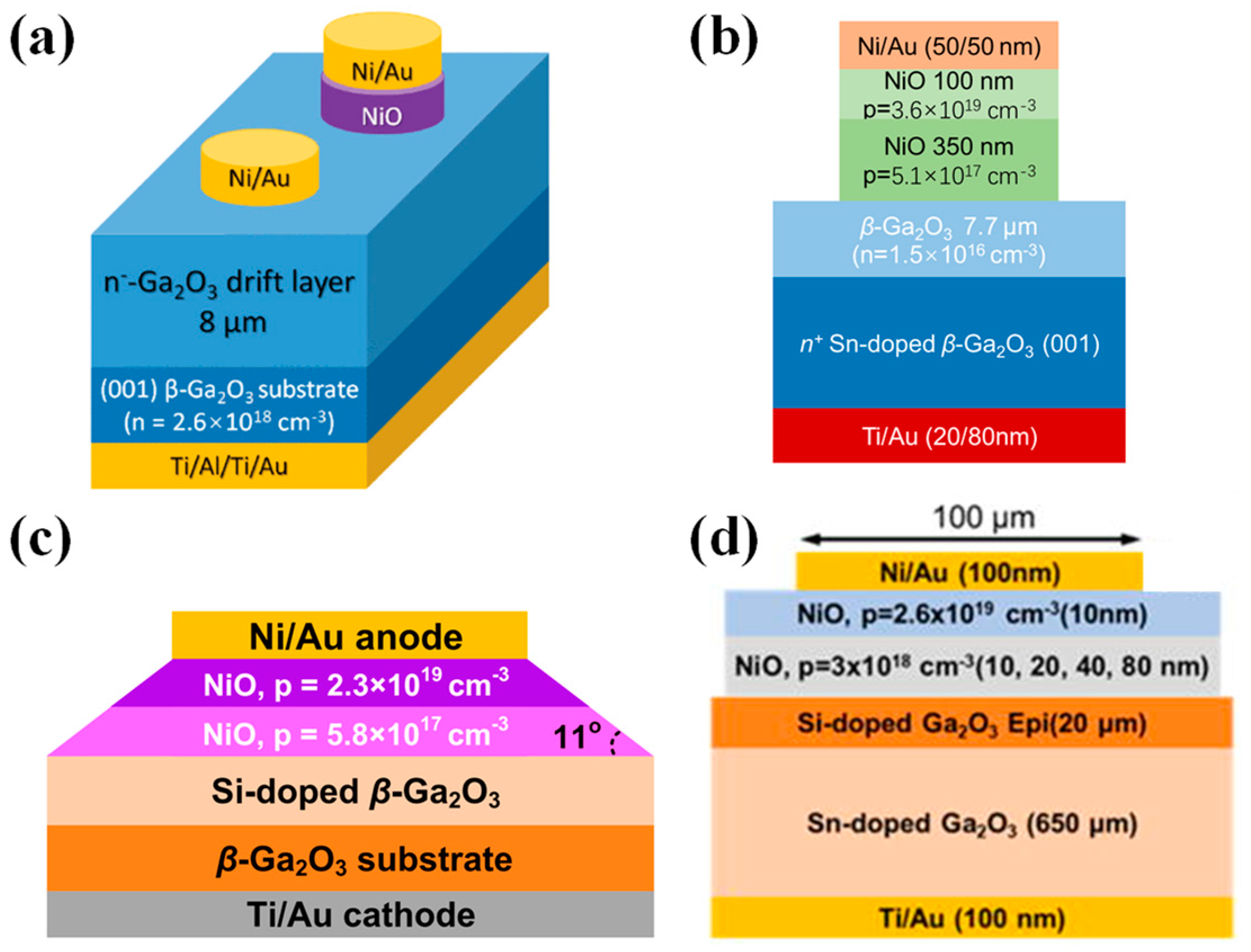
4.2.1. Heterojunction Diodes

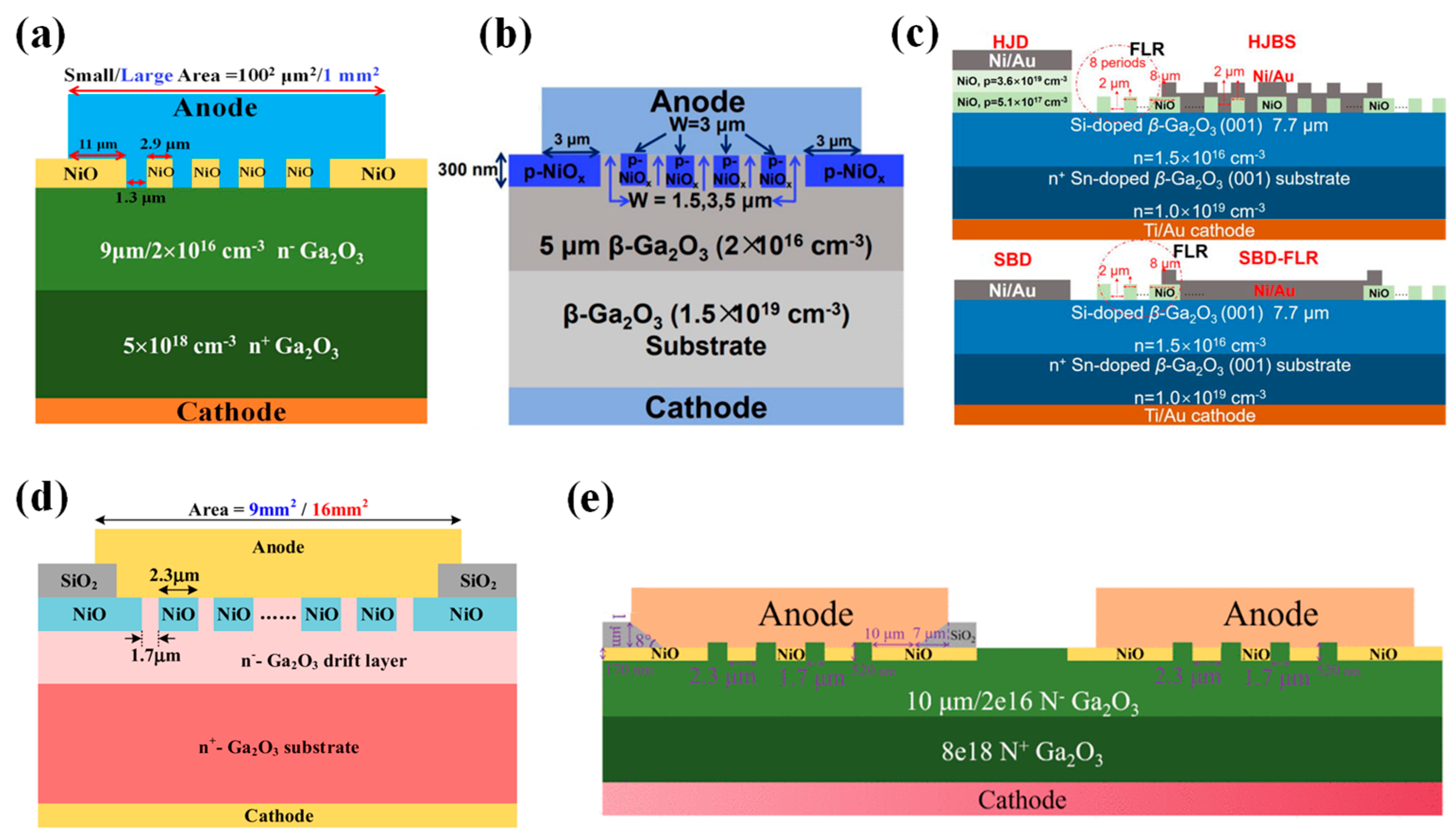
4.2.2. Heterojunction Barrier Schottky Diodes
4.2.3. Junction Termination Extension Structures and Super Junction SBDs
4.3. Lateral-Structure Diodes
4.4. Summary
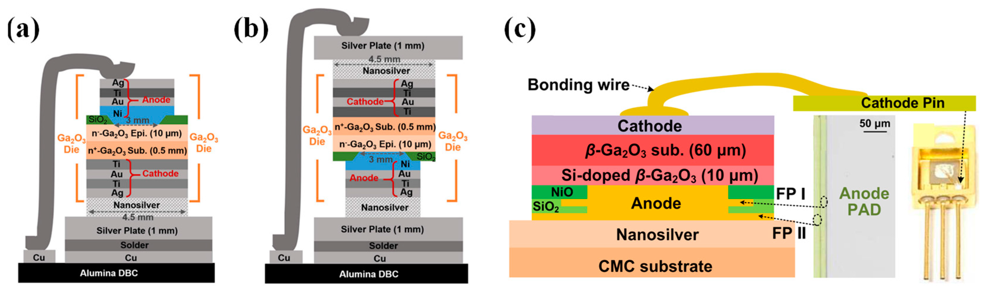
5. Surge Current Ruggedness and Thermal Management
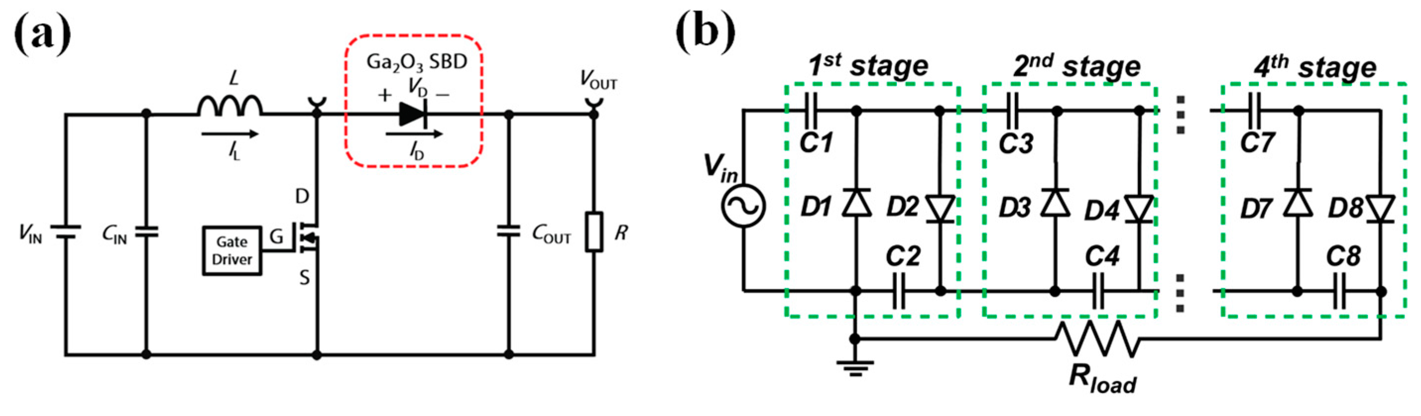
6. Circuit Application and Reliability
7. Summary and Prospect
- (a)
- The development of iridium-free β-Ga2O3 single-crystal manufacturing technologies and the improvement of crystal quality will greatly facilitate the practical application of β-Ga2O3.
- (b)
- The mobility of NiO layers prepared by sputtering is significantly lower compared to β-Ga2O3, which limits the performance of HJDs to some extent. The realization of effective p-type doped Ga2O3, or developing alternative high-performance p-type materials, will further enhance the performance of β-Ga2O3 HJDs.
- (c)
- Due to the very low thermal conductivity of β-Ga2O3 materials, there is still a need for better β-Ga2O3 thermal management methods and further research on device reliability.
Author Contributions
Funding
Data Availability Statement
Conflicts of Interest
References
- Perreault, D.J.; Hu, J.; Rivas, J.M.; Han, Y.; Leitermann, O.; Pilawa-Podgurski, R.C.N.; Sagneri, A.; Sullivan, C.R. Opportunities and Challenges in Very High Frequency Power Conversion. In Proceedings of the 24th Annual IEEE Applied Power Electronics Conference and Exposition, Washington, DC, USA, 15–19 February 2009. [Google Scholar]
- Filchev, T.; Carastro, F.; Wheeler, P.; Clare, J. High Voltage High Frequency Power Transformer for Pulsed Power Application. In Proceedings of the 14th International Power Electronics and Motion Control Conference (EPE-PEMC), Ohrid, Macedonia, 6–8 September 2010; pp. 165–170. [Google Scholar]
- Mao, S.; Wu, T.; Lu, X.; Popovic, J.; Ferreira, J.A. High Frequency High Voltage Power Conversion with Silicon Carbide Power Semiconductor Devices. In Proceedings of the 6th Electronic System-Integration Technology Conference (ESTC), Grenoble, France, 13–16 September 2016. [Google Scholar]
- Dong, D.; Lin, X.; Ravi, L.; Yan, N.; Burgos, R. Advancement of SiC High-frequency Power Conversion Systems for Medium-Voltage High-Power Applications. In Proceedings of the IEEE 9th International Power Electronics and Motion Control Conference (IPEMC-ECCE Asia), Nanjing, China, 29 November–2 December 2020; pp. 717–724. [Google Scholar]
- Hazra, S.; De, A.; Cheng, L.; Palmour, J.; Schupbach, M.; Hull, B.A.; Allen, S.; Bhattacharya, S. High Switching Performance of 1700-V, 50-A SiC Power MOSFET Over Si IGBT/BiMOSFET for Advanced Power Conversion Applications. IEEE Trans. Power Electron. 2016, 31, 4742–4754. [Google Scholar]
- Zhang, L.; Yuan, X.; Wu, X.; Shi, C.; Zhang, J.; Zhang, Y. Performance Evaluation of High-Power SiC MOSFET Modules in Comparison to Si IGBT Modules. IEEE Trans. Power Electron. 2019, 34, 1181–1196. [Google Scholar] [CrossRef]
- Rujas, A.; Lopez, V.M.; Garcia-Bediaga, A.; Berasategi, A.; Nieva, T. Railway traction DC-DC converter: Comparison of Si, SiC-hybrid, and full SiC versions with 1700 V power modules. IET Power Electron. 2019, 12, 3265–3271. [Google Scholar] [CrossRef]
- She, X.; Huang, A.Q.; Lucia, O.; Ozpineci, B. Review of Silicon Carbide Power Devices and Their Applications. IEEE Trans. Ind. Electron. 2017, 64, 8193–8205. [Google Scholar] [CrossRef]
- He, J.; Cheng, W.C.; Wang, Q.; Cheng, K.; Yu, H.; Chai, Y. Recent Advances in GaN-Based Power HEMT Devices. Adv. Electron. Mater. 2021, 7, 2001045. [Google Scholar] [CrossRef]
- Powell, A.R.; Rowland, L.B. SiC materials-Progress, status, and potential roadblocks. Proc. IEEE 2002, 90, 942–955. [Google Scholar] [CrossRef]
- Paskova, T.; Evans, K.R. GaN Substrates-Progress, Status, and Prospects. IEEE J. Sel. Top. Quantum Electron. 2009, 15, 1041–1052. [Google Scholar] [CrossRef]
- Coffa, S.; Saggio, M.; Patti, A. SiC- and GaN-based power devices: Technologies, products and applications. In Proceedings of the IEEE International Electron Devices Meeting (IEDM), Washington, DC, USA, 7–9 December 2015; pp. 438–442. [Google Scholar]
- Roy, R.; Hill, V.G.; Osborn, E.F. Polymorphism of Ga2O3 and the system Ga2O3-H2O. J. Am. Chem. Soc. 1952, 74, 719–722. [Google Scholar] [CrossRef]
- Yoshioka, S.; Hayashi, H.; Kuwabara, A.; Oba, F.; Matsunaga, K.; Tanaka, I. Structures and energetics of Ga2O3 polymorphs. J. Phys. Condens. Matter 2007, 19, 346211. [Google Scholar] [CrossRef]
- Galazka, Z.; Irmscher, K.; Uecker, R.; Bertram, R.; Pietsch, M.; Kwasniewski, A.; Naumann, M.; Schulz, T.; Schewski, R.; Klimm, D.; et al. On the bulk β-Ga2O3 single crystals grown by the Czochralski method. J. Cryst. Growth 2014, 404, 184–191. [Google Scholar] [CrossRef]
- Oishi, T.; Koga, Y.; Harada, K.; Kasu, M. High-mobility β-Ga2O3 (01) single crystals grown by edge-defined film-fed growth method and their Schottky barrier diodes with Ni contact. Appl. Phys. Express 2015, 8, 031101. [Google Scholar] [CrossRef]
- Kuramata, A.; Koshi, K.; Watanabe, S.; Yamaoka, Y.; Masui, T.; Yamakoshi, S. High-quality β-Ga2O3 single crystals grown by edge-defined film-fed growth. Jpn. J. Appl. Phys. 2016, 55, 1202A1202. [Google Scholar] [CrossRef]
- Galazka, Z.; Uecker, R.; Klimm, D.; Irmscher, K.; Naumann, M.; Pietsch, M.; Kwasniewski, A.; Bertram, R.; Ganschow, S.; Bickermann, M. Scaling-Up of Bulk β-Ga2O3 Single Crystals by the Czochralski Method. ECS J. Solid State Sci. Technol. 2017, 6, Q3007–Q3011. [Google Scholar] [CrossRef]
- Pearton, S.J.; Yang, J.; Cary, P.H.; Ren, F.; Kim, J.; Tadjer, M.J.; Mastro, M.A. A review of Ga2O3 materials, processing, and devices. Appl. Phys. Rev. 2018, 5, 011301. [Google Scholar] [CrossRef]
- Reese, S.B.; Remo, T.; Green, J.; Zakutayev, A.J.J. How much will gallium oxide power electronics cost? Joule 2019, 3, 903–907. [Google Scholar] [CrossRef]
- Heinselman, K.N.; Haven, D.; Zakutayev, A.; Reese, S.B. Projected Cost of Gallium Oxide Wafers from Edge-Defined Film-Fed Crystal Growth. Cryst. Growth Des. 2022, 22, 4854–4863. [Google Scholar] [CrossRef]
- The World’s First Practical-Size Gallium Oxide Single Crystals Are Successfully Grown without Precious Metal Crucibles. Available online: https://www.c-and-a.jp/assets/img/News/20220404PressRelease.pdf (accessed on 4 April 2022).
- Higashiwaki, M.; Murakami, H.; Kumagai, Y.; Kuramata, A. Current status of Ga2O3 power devices. Jpn. J. Appl. Phys. 2016, 55, 1202A1. [Google Scholar] [CrossRef]
- Higashiwaki, M.; Kuramata, A.; Murakami, H.; Kumagai, Y. State-of-the-art technologies of gallium oxide power devices. J. Phys. D-Appl. Phys. 2017, 50, 333002. [Google Scholar] [CrossRef]
- Kaur, D.; Ghosh, A.; Kumar, M. A strategic review on gallium oxide based power electronics: Recent progress and future prospects. Mater. Today Commun. 2022, 33, 104244. [Google Scholar] [CrossRef]
- Prasad, C.V.; Rim, Y.S. Review on interface engineering of low leakage current and on-resistance for high-efficiency Ga2O3-based power devices. Mater. Today Phys. 2022, 27, 100777. [Google Scholar] [CrossRef]
- Lyons, J.L. A survey of acceptor dopants for β-Ga2O3. Semicond. Sci. Technol. 2018, 33, 05LT02. [Google Scholar] [CrossRef]
- Wong, M.H.; Lin, C.H.; Kuramata, A.; Yamakoshi, S.; Murakami, H.; Kumagai, Y.; Higashiwaki, M. Acceptor doping of β-Ga2O3 by Mg and N ion implantations. Appl. Phys. Lett. 2018, 113, 102103. [Google Scholar] [CrossRef]
- Su, Y.L.; Guo, D.Y.; Ye, J.H.; Zhao, H.L.; Wang, Z.; Wang, S.L.; Li, P.G.; Tang, W.H. Deep level acceptors of Zn-Mg divalent ions dopants in β-Ga2O3 for the difficulty to p-type conductivity. J. Alloys Compd. 2019, 782, 299–303. [Google Scholar] [CrossRef]
- Li, L.; Liao, F.; Hu, X. The possibility of N-P codoping to realize P type β-Ga2O3. Superlattices Microstruct. 2020, 141, 106502. [Google Scholar] [CrossRef]
- Kananen, B.E.; Giles, N.C.; Halliburton, L.E.; Foundos, G.K.; Chang, K.B.; Stevens, K.T. Self-trapped holes in β-Ga2O3 crystals. J. Appl. Phys. 2017, 122, 215703. [Google Scholar] [CrossRef]
- Gake, T.; Kumagai, Y.; Oba, F. First-principles study of self-trapped holes and acceptor impurities in Ga2O3 polymorphs. Phys. Rev. Mater. 2019, 3, 044603. [Google Scholar] [CrossRef]
- Liu, Z.; Li, P.G.; Zhi, Y.S.; Wang, X.L.; Chu, X.L.; Tang, W.H. Review of gallium oxide based field-effect transistors and Schottky barrier diodes. Chin. Phys. B 2019, 28, 017105. [Google Scholar] [CrossRef]
- Ji, X.; Lu, C.; Yan, Z.; Shan, L.; Yan, X.; Wang, J.; Yue, J.; Qi, X.; Liu, Z.; Tang, W.; et al. A review of gallium oxide-based power Schottky barrier diodes. J. Phys. D-Appl. Phys. 2022, 55, 443002. [Google Scholar] [CrossRef]
- Qiao, R.; Zhang, H.; Zhao, S.; Yuan, L.; Jia, R.; Peng, B.; Zhang, Y. A state-of-art review on gallium oxide field-effect transistors. J. Phys. D-Appl. Phys. 2022, 55, 383003. [Google Scholar] [CrossRef]
- Sasaki, K.; Kuramata, A.; Masui, T.; Villora, E.G.; Shimamura, K.; Yamakoshi, S. Device-Quality β-Ga2O3 Epitaxial Films Fabricated by Ozone Molecular Beam Epitaxy. Appl. Phys. Express 2012, 5, 035502. [Google Scholar] [CrossRef]
- Qin, Y.; Xiao, M.; Porter, M.; Ma, Y.; Spencer, J.; Du, Z.; Jacobs, A.G.; Sasaki, K.; Wang, H.; Tadjer, M.; et al. 10-kV Ga2O3 Charge-Balance Schottky Rectifier Operational at 200 °C. IEEE Electron Device Lett. 2023, 44, 1268–1271. [Google Scholar] [CrossRef]
- Wang, C.; Yan, Q.; Zhang, C.; Su, C.; Zhang, K.; Sun, S.; Liu, Z.; Zhang, W.; Alghamdi, S.; Ghandourah, E.; et al. β-Ga2O3 Lateral Schottky Barrier Diodes With >10 kV Breakdown Voltage and Anode Engineering. IEEE Electron Device Lett. 2023, 44, 1684–1687. [Google Scholar] [CrossRef]
- Zhang, J.; Dong, P.; Dang, K.; Zhang, Y.; Yan, Q.; Xiang, H.; Su, J.; Liu, Z.; Si, M.; Gao, J.; et al. Ultra-wide bandgap semiconductor Ga2O3 power diodes. Nat. Commun. 2022, 13, 3900. [Google Scholar] [CrossRef] [PubMed]
- The World’s First Ampere-Class 1200-V Breakdown-Voltage Gallium Oxide Schottky Barrier Diode. Available online: https://www.novelcrystal.co.jp/eng/2021/1048/ (accessed on 24 December 2021).
- Kim, S.H.; Yang, M.; Lee, H.-Y.; Choi, J.-S.; Lee, H.U.; Kim, U.J.; Lee, M. Structural characteristics of α-Ga2O3 films grown on sapphire by halide vapor phase epitaxy. Mater. Sci. Semicond. Process. 2021, 123, 105534. [Google Scholar] [CrossRef]
- Polyakov, A.; Nikolaev, V.; Stepanov, S.; Almaev, A.; Pechnikov, A.; Yakimov, E.; Kushnarev, B.O.; Shchemerov, I.; Scheglov, M.; Chernykh, A.; et al. Electrical properties of α-Ga2O3 films grown by halide vapor phase epitaxy on sapphire with α-Cr2O3 buffers. J. Appl. Phys. 2022, 131, 215701. [Google Scholar] [CrossRef]
- Yang, D.; Kim, B.; Oh, J.; Lee, T.H.; Ryu, J.; Park, S.; Kim, S.; Yoon, E.; Park, Y.; Jang, H.W. α-Gallium Oxide Films on Microcavity-Embedded Sapphire Substrates Grown by Mist Chemical Vapor Deposition for High-Breakdown Voltage Schottky Diodes. ACS Appl. Mater. Interfaces 2022, 14, 5598–5607. [Google Scholar] [CrossRef] [PubMed]
- Boldbaatar, S.; Janardhanam, V.; Zumuukhorol, M.; Lee, H.K.; Lee, H.Y.; Kim, H.J.; Shim, K.H.; Choi, C.J. Temperature-dependent Schottky diode behavior of Ni Schottky contacts to α-Ga2O3 film epitaxially grown on sapphire substrate. Mater. Sci. Semicond. Process. 2023, 163, 107589. [Google Scholar] [CrossRef]
- Oda, M.; Kikawa, J.; Takatsuka, A.; Tokuda, R.; Sasaki, T.; Kaneko, K.; Fujita, S.; Hitora, T. Vertical Schottky Barrier Diodes of α-Ga2O3 Fabricated by Mist Epitaxy. In Proceedings of the 2015 73rd Annual Device Research Conference (DRC), Ohio State University, Columbus, OH, USA, 21–24 June 2015; pp. 137–138. [Google Scholar]
- Oda, M.; Tokuda, R.; Kambara, H.; Tanikawa, T.; Sasaki, T.; Hitora, T. Schottky barrier diodes of corundum-structured gallium oxide showing on-resistance of 0.1 mΩ·cm2 grown by MIST EPITAXY®. Appl. Phys. Express 2016, 9, 021101. [Google Scholar] [CrossRef]
- Shinohe, T. Development of Corundum-Structured Gallium Oxide Power Devices by MIST EPITAXY®. In Proceedings of the IEEE International Meeting for Future of Electron Devices, Kansai (IMFEDK), Kyoto, Japan, 21–22 June 2018; pp. 1–2. [Google Scholar]
- Kaneko, K.; Fujita, S.; Hitora, T. A power device material of corundum-structured α-Ga2O3 fabricated by MIST EPITAXY® technique. Jpn. J. Appl. Phys. 2018, 57, 02CB18. [Google Scholar] [CrossRef]
- Succeeded in Developing the World’s First Ampere-Class, 1700 V Corundum-Type Gallium Oxide SBD! Available online: https://flosfia.com/20230303/ (accessed on 3 March 2023).
- Zhang, X.; Zhang, Z.; Liang, J.; Zhou, Y.; Tong, Y.; Wang, Y.; Wang, X. Freestanding single layers of non-layered material γ-Ga2O3 as an efficient photocatalyst for overall water splitting. J. Mater. Chem. A 2017, 5, 9702–9708. [Google Scholar] [CrossRef]
- Zhang, X.; Huang, H.; Zhang, Y.; Liu, D.; Tong, N.; Lin, J.; Chen, L.; Zhang, Z.; Wang, X. Phase Transition of Two-Dimensional β-Ga2O3 Nanosheets from Ultrathin γ-Ga2O3 Nanosheets and Their Photocatalytic Hydrogen Evolution Activities. ACS Omega 2018, 3, 14469–14476. [Google Scholar] [CrossRef] [PubMed]
- Huang, H.; Shen, J.; Liu, X.; Zhong, Y.; Zhang, Z.; Wang, X. Self-assembly of Ni2P/γ-Ga2O3 nanosheets for efficient photocatalytic water splitting hydrogen production. Dalton Trans. 2022, 51, 17836–17843. [Google Scholar] [CrossRef] [PubMed]
- Shen, J.; Liu, X.; Zhong, Y.; Qiu, C.; Xu, H.; He, H.; Li, H.; Lin, J.; Zhang, Z.; Wang, X. Photocatalytic Overall Water Splitting Reaction Feature on Photodeposited NixP/γ-Ga2O3 Nanosheets. ACS Appl. Energy Mater. 2023, 6, 4317–4326. [Google Scholar] [CrossRef]
- Cho, S.B.; Mishra, R. Epitaxial engineering of polar ε-Ga2O3 for tunable two-dimensional electron gas at the heterointerface. Appl. Phys. Lett. 2018, 112, 162101. [Google Scholar] [CrossRef]
- Wang, J.; Guo, H.; Zhu, C.; Cai, Q.; Yang, G.; Xue, J.; Chen, D.; Tong, Y.; Liu, B.; Lu, H.; et al. ε-Ga2O3: A Promising Candidate for High-electron-Mobility Transistors. IEEE Electron Device Lett. 2020, 41, 1052–1055. [Google Scholar] [CrossRef]
- Cora, I.; Mezzadri, F.; Boschi, F.; Bosi, M.; Caplovicova, M.; Calestani, G.; Dodony, I.; Pecz, B.; Fornari, R. The real structure of ε-Ga2O3 and its relation to κ-phase. CrystEngComm 2017, 19, 1509–1516. [Google Scholar] [CrossRef]
- Dobrocka, E.; Gucmann, F.; Husekova, K.; Nadazdy, P.; Hrubisak, F.; Egyenes, F.; Rosova, A.; Mikolasek, M.; Tapajna, M. Structure and Thermal Stability of ε/κ-Ga2O3 Films Deposited by Liquid-Injection MOCVD. Materials 2023, 16, 20. [Google Scholar] [CrossRef] [PubMed]
- Lee, J.; Kim, H.; Gautam, L.; Razeghi, M. High Thermal Stability of κ-Ga2O3 Grown by MOCVD. Crystals 2021, 11, 446. [Google Scholar] [CrossRef]
- Girolami, M.; Bosi, M.; Serpente, V.; Mastellone, M.; Seravalli, L.; Pettinato, S.; Salvatori, S.; Trucchi, D.M.M.; Fornari, R. Orthorhombic undoped κ-Ga2O3 epitaxial thin films for sensitive, fast, and stable direct X-ray detectors. J. Mater. Chem. C 2023, 11, 3759–3769. [Google Scholar] [CrossRef]
- Lim, N.; Min, J.; Min, J.H.; Kang, C.H.; Li, K.H.; Park, T.Y.; Kim, W.; Davaasuren, B.; Ng, T.K.; Ooi, B.S.; et al. Ultrasensitive UV-C detection based on MOCVD-grown highly crystalline ultrawide bandgap orthorhombic κ-Ga2O3. Appl. Surf. Sci. 2023, 609, 155350. [Google Scholar] [CrossRef]
- Kang, H.Y.; Kang, H.; Lee, E.; Lee, G.R.; Chung, R.B.K. Sn-Induced Phase Stabilization and Enhanced Thermal Stability of κ-Ga2O3 Grown by Mist Chemical Vapor Deposition. ACS Omega 2021, 6, 31292–31298. [Google Scholar] [CrossRef] [PubMed]
- Peelaers, H.; Van de Walle, C.G. Lack of quantum confinement in Ga2O3 nanolayers. Phys. Rev. B 2017, 96, 081409. [Google Scholar] [CrossRef]
- Feng, W.; Wang, X.; Zhang, J.; Wang, L.; Zheng, W.; Hu, P.; Cao, W.; Yang, B. Synthesis of two-dimensional β-Ga2O3 nanosheets for high-performance solar blind photodetectors. J. Mater. Chem. C 2014, 2, 3254–3259. [Google Scholar] [CrossRef]
- Su, J.; Zhang, J.; Guo, R.; Lin, Z.; Liu, M.; Zhang, J.; Chang, J.; Hao, Y. Mechanical and thermodynamic properties of two-dimensional monoclinic Ga2O3. Mater. Des. 2019, 184, 108197. [Google Scholar] [CrossRef]
- Guo, R.; Su, J.; Yuan, H.; Zhang, P.; Lin, Z.; Zhang, J.; Chang, J.; Hao, Y. Surface functionalization modulates the structural and optoelectronic properties of two-dimensional Ga2O3. Mater. Today Phys. 2020, 12, 100192. [Google Scholar] [CrossRef]
- Deng, Z. Predicting the Raman spectra of ferroelectric phases in two-dimensional Ga2O3 monolayer. Phys. Chem. Chem. Phys. 2022, 24, 13671–13677. [Google Scholar] [CrossRef] [PubMed]
- Seyidov, P.; Varley, J.B.; Frodason, Y.K.; Klimm, D.; Vines, L.; Galazka, Z.; Chou, T.S.; Popp, A.; Irmscher, K.; Fiedler, A. Thermal Stability of Schottky Contacts and Rearrangement of Defects in β-Ga2O3 Crystals. Adv. Electron. Mater. 2023, 2300428. [Google Scholar] [CrossRef]
- Hossain, E.; Kulkarni, R.; Mondal, R.; Guddolian, S.; Rahman, A.A.; Thamizhavel, A.; Bhattacharya, A. Optimization of Gas Ambient for High Quality β-Ga2O3 Single Crystals Grown by the Optical Floating Zone Technique. ECS J. Solid State Sci. Technol. 2019, 8, Q3144–Q3148. [Google Scholar] [CrossRef]
- Fujita, Y.; Nagao, M.; Maruyama, Y.; Watauchi, S.; Miki, K.; Tanaka, I. Solubility of iridium into β-Ga2O3 single crystals grown by floating zone method. J. Cryst. Growth 2022, 584, 126581. [Google Scholar] [CrossRef]
- Perrier, C.; Traore, A.; Ito, T.; Umezawa, H.; Gheeraert, E.; Ferrandis, P. Surface defects related to polishing cycle in β-Ga2O3 crystals grown by floating zone. Appl. Phys. Lett. 2023, 122, 222105. [Google Scholar] [CrossRef]
- Hoshikawa, K.; Ohba, E.; Kobayashi, T.; Yanagisawa, J.; Miyagawa, C.; Nakamura, Y. Growth of β-Ga2O3 single crystals using vertical Bridgman method in ambient air. J. Cryst. Growth 2016, 447, 36–41. [Google Scholar] [CrossRef]
- Hoshikawa, K.; Kobayashi, T.; Matsuki, Y.; Ohba, E. 2-inch diameter (100) β-Ga2O3 crystal growth by the vertical Bridgman technique in a resistance heating furnace in ambient air. J. Cryst. Growth 2020, 545, 125724. [Google Scholar] [CrossRef]
- Ohba, E.; Kobayashi, T.; Taishi, T.; Hoshikawa, K. Growth of (100), (010) and (001) β-Ga2O3 single crystals by vertical Bridgman method. J. Cryst. Growth 2021, 556, 125990. [Google Scholar] [CrossRef]
- Mu, W.; Jia, Z.; Yin, Y.; Hu, Q.; Li, Y.; Wu, B.; Zhang, J.; Tao, X. High quality crystal growth and anisotropic physical characterization of β-Ga2O3 single crystals grown by EFG method. J. Alloys Compd. 2017, 714, 453–458. [Google Scholar] [CrossRef]
- Yao, Y.; Ishikawa, Y.; Sugawara, Y. Revelation of Dislocations in β-Ga2O3 Substrates Grown by Edge-Defined Film-Fed Growth. Phys. Status Solidi A-Appl. Mater. Sci. 2020, 217, 1900630. [Google Scholar] [CrossRef]
- Fu, B.; Jian, G.; Mu, W.; Li, Y.; Wang, H.; Jia, Z.; Li, Y.; Long, S.; Shi, Y.; Tao, X. Crystal growth and design of Sn-doped β-Ga2O3: Morphology, defect and property studies of cylindrical crystal by EFG. J. Alloys Compd. 2022, 896, 162830. [Google Scholar] [CrossRef]
- Bauman, D.A.; Iu Panov, D.; Spiridonov, V.A.; Kremleva, A.V.; Asach, A.V.; Tambulatova, E.V.; Sakharov, A.V.; Romanov, A.E. High quality β-Ga2O3 bulk crystals, grown by edge-defined film-fed growth method: Growth features, structural, and thermal properties. J. Vac. Sci. Technol. A 2023, 41, 053203. [Google Scholar] [CrossRef]
- Pratiyush, A.S.; Xia, Z.; Kumar, S.; Zhang, Y.; Joishi, C.; Muralidharan, R.; Rajan, S.; Nath, D.N. MBE-Grown β-Ga2O3-Based Schottky UV-C Photodetectors With Rectification Ratio ∼107. IEEE Photonics Technol. Lett. 2018, 30, 2025–2028. [Google Scholar] [CrossRef]
- Brooks Tellekamp, M.; Heinselman, K.N.; Harvey, S.; Khan, I.S.; Zakutayev, A. Growth and characterization of homoepitaxial β-Ga2O3 layers. J. Phys. D-Appl. Phys. 2020, 53, 484002. [Google Scholar] [CrossRef]
- Vogt, P.; Hensling, F.V.E.; Azizie, K.; Chang, C.S.; Turner, D.; Park, J.; McCandless, J.P.; Paik, H.; Bocklund, B.J.; Hoffman, G.; et al. Adsorption-controlled growth of Ga2O3 by suboxide molecular-beam epitaxy. APL Mater. 2021, 9, 031101. [Google Scholar] [CrossRef]
- Xiu, X.; Zhang, L.; Li, Y.; Xiong, Z.; Zhang, R.; Zheng, Y. Application of halide vapor phase epitaxy for the growth of ultra-wide band gap Ga2O3. J. Semicond. 2019, 40, 011805. [Google Scholar] [CrossRef]
- Sdoeung, S.; Sasaki, K.; Masuya, S.; Kawasaki, K.; Hirabayashi, J.; Kuramata, A.; Kasu, M. Stacking faults: Origin of leakage current in halide vapor phase epitaxial (001) β-Ga2O3 Schottky barrier diodes. Appl. Phys. Lett. 2021, 118, 172106. [Google Scholar] [CrossRef]
- Sdoeung, S.; Sasaki, K.; Kawasaki, K.; Hirabayashi, J.; Kuramata, A.; Oishi, T.; Kasu, M. Line-shaped defects: Origin of leakage current in halide vapor-phase epitaxial (001) β-Ga2O3 Schottky barrier diodes. Appl. Phys. Lett. 2022, 120, 122107. [Google Scholar] [CrossRef]
- Sdoeung, S.; Otsubo, Y.; Sasaki, K.; Kuramata, A.; Kasu, M. Killer defect responsible for reverse leakage current in halide vapor phase epitaxial (011) β-Ga2O3 Schottky barrier diodes investigated via ultrahigh sensitive emission microscopy and synchrotron x-ray topography. Appl. Phys. Lett. 2023, 123, 122101. [Google Scholar] [CrossRef]
- Ji, X.; Yue, J.; Qi, X.; Yan, Z.; Li, S.; Lu, C.; Li, Z.; Liu, Z.; Qi, S.; Yan, X.; et al. Homoepitaxial Si-doped Gallium Oxide films by MOCVD with tunable electron concentrations and electrical properties. Vacuum 2023, 210, 111902. [Google Scholar] [CrossRef]
- Sood, A.; Wuu, D.S.; Tarntair, F.G.; Sao, N.T.; Wu, T.L.; Tumilty, N.; Kuo, H.C.; Pratap, S.J.; Horng, R.H. Electrical performance study of Schottky barrier diodes using ion implanted β-Ga2O3 epilayers grown on sapphire substrates. Mater. Today Adv. 2023, 17, 100346. [Google Scholar] [CrossRef]
- Sundaram, P.P.; Liu, F.; Alema, F.; Osinsky, A.; Jalan, B.; Koester, S.J. Characterization of (001) β-Ga2O3 Schottky diodes with drift layer grown by MOCVD. Appl. Phys. Lett. 2023, 122, 232105. [Google Scholar] [CrossRef]
- Khartsev, S.; Nordell, N.; Hammar, M.; Purans, J.; Hallen, A. High-Quality Si-Doped β-Ga2O3 Films on Sapphire Fabricated by Pulsed Laser Deposition. Phys. Status Solidi B-Basic Solid State Phys. 2021, 258, 2000362. [Google Scholar] [CrossRef]
- Khartsev, S.; Hammar, M.; Nordell, N.; Zolotarjovs, A.; Purans, J.; Hallen, A. Reverse-Bias Electroluminescence in Er-Doped β-Ga2O3 Schottky Barrier Diodes Manufactured by Pulsed Laser Deposition. Phys. Status Solidi A-Appl. Mater. Sci. 2022, 219, 2100610. [Google Scholar] [CrossRef]
- Koepp, S.; Petersen, C.; Splith, D.; Grundmann, M.; von Wenckstern, H. Properties of Schottky barrier diodes on heteroeptixial α-Ga2O3 thin films. J. Vac. Sci. Technol. A 2023, 41, 043411. [Google Scholar] [CrossRef]
- Zhang, Y.; Feng, Z.; Karim, M.R.; Zhao, H. High-temperature low-pressure chemical vapor deposition of β-Ga2O3. J. Vac. Sci. Technol. A 2020, 38, 050806. [Google Scholar] [CrossRef]
- Saha, S.; Meng, L.; Feng, Z.; Anhar Uddin Bhuiyan, A.F.M.; Zhao, H.; Singisetti, U. Schottky diode characteristics on high-growth rate LPCVD β-Ga2O3 films on (010) and (001) Ga2O3 substrates. Appl. Phys. Lett. 2022, 120, 122106. [Google Scholar] [CrossRef]
- Ghadi, H.; McGlone, J.F.; Cornuelle, E.; Feng, Z.; Zhang, Y.; Meng, L.; Zhao, H.; Arehart, A.R.; Ringel, S.A. Deep level defects in low-pressure chemical vapor deposition grown (010) β-Ga2O3. APL Mater. 2022, 10, 101110. [Google Scholar] [CrossRef]
- Dang, G.T.; Kawaharamura, T.; Furuta, M.; Allen, M.W. Mist-CVD Grown Sn-Doped α-Ga2O3 MESFETs. IEEE Trans. Electron Devices 2015, 62, 3640–3644. [Google Scholar] [CrossRef]
- Maeda, T.; Okigawa, M.; Kato, Y.; Takahashi, I.; Shinohe, T. Defect-insensitive current-voltage characteristics of Schottky barrier diode formed on heteroepitaxial α-Ga2O3 grown by mist chemical vapor deposition. AIP Adv. 2020, 10, 125119. [Google Scholar] [CrossRef]
- Yuan, Y.; Hao, W.; Mu, W.; Wang, Z.; Chen, X.; Liu, Q.; Xu, G.; Wang, C.; Zhou, H.; Zou, Y.; et al. Toward emerging gallium oxide semiconductors: A roadmap. Fundam. Res. 2021, 1, 697–716. [Google Scholar] [CrossRef]
- Chen, X.; Ren, F.; Gu, S.; Ye, J. Review of gallium-oxide-based solar-blind ultraviolet photodetectors. Photonics Res. 2019, 7, 381–415. [Google Scholar] [CrossRef]
- Guo, D.; Guo, Q.; Chen, Z.; Wu, Z.; Li, P.; Tang, W. Review of Ga2O3-based optoelectronic devices. Mater. Today Phys. 2019, 11, 100157. [Google Scholar] [CrossRef]
- Xu, J.; Zheng, W.; Huang, F. Gallium oxide solar-blind ultraviolet photodetectors: A review. J. Mater. Chem. C 2019, 7, 8753–8770. [Google Scholar] [CrossRef]
- Wu, C.; Wu, F.; Hu, H.; Wang, S.; Liu, A.; Guo, D. Review of self-powered solar-blind photodetectors based on Ga2O3. Mater. Today Phys. 2022, 28, 100883. [Google Scholar] [CrossRef]
- Tsao, J.Y.; Chowdhury, S.; Hollis, M.A.; Jena, D.; Johnson, N.M.; Jones, K.A.; Kaplar, R.J.; Rajan, S.; Van de Walle, C.G.; Bellotti, E.; et al. Ultrawide-Bandgap Semiconductors: Research Opportunities and Challenges. Adv. Electron. Mater. 2018, 4, 1600501. [Google Scholar] [CrossRef]
- Yang, J.; Liu, K.; Chen, X.; Shen, D. Recent advances in optoelectronic and microelectronic devices based on ultrawide-bandgap semiconductors. Prog. Quantum Electron. 2022, 83, 100397. [Google Scholar] [CrossRef]
- Matsumae, T.; Kurashima, Y.; Umezawa, H.; Tanaka, K.; Ito, T.; Watanabe, H.; Takagi, H. Low-temperature direct bonding of β-Ga2O3 and diamond substrates under atmospheric conditions. Appl. Phys. Lett. 2020, 116, 141602. [Google Scholar] [CrossRef]
- Sittimart, P.; Ohmagari, S.; Matsumae, T.; Umezawa, H.; Yoshitake, T. Diamond/β-Ga2O3 pn heterojunction diodes fabricated by low-temperature direct-bonding. AIP Adv. 2021, 11, 105114. [Google Scholar] [CrossRef]
- Lu, X.; Deng, Y.; Pei, Y.; Chen, Z.; Wang, G. Recent advances in NiO/Ga2O3 heterojunctions for power electronics. J. Semicond. 2023, 44, 061802. [Google Scholar] [CrossRef]
- Ghosh, K.; Singisetti, U. Ab initio velocity-field curves in monoclinic β-Ga2O3. J. Appl. Phys. 2017, 122, 035702. [Google Scholar] [CrossRef]
- Zhang, Y.; Xia, Z.; McGlone, J.; Sun, W.; Joishi, C.; Arehart, A.R.; Ringel, S.A.; Rajan, S. Evaluation of Low-Temperature Saturation Velocity in β-(AlxGa1-x)2O3/Ga2O3 Modulation-Doped Field-Effect Transistors. IEEE Trans. Electron Devices 2019, 66, 1574–1578. [Google Scholar] [CrossRef]
- Lu, C.; Ji, X.; Liu, Z.; Yan, X.; Lu, N.; Li, P.; Tang, W. A review of metal-semiconductor contacts for β-Ga2O3. J. Phys. D-Appl. Phys. 2022, 55, 463002. [Google Scholar] [CrossRef]
- Mott, N.F. Metal-insulator transltion. Rev. Mod. Phys. 1968, 40, 1039–1263. [Google Scholar] [CrossRef]
- Huan, Y.W.; Sun, S.M.; Gu, C.J.; Liu, W.J.; Ding, S.J.; Yu, H.Y.; Xia, C.T.; Zhang, D.W. Recent Advances in β-Ga2O3-Metal Contacts. Nanoscale Res. Lett. 2018, 13, 246. [Google Scholar] [CrossRef]
- Lyle, L.A.M. Critical review of Ohmic and Schottky contacts to β-Ga2O3. J. Vac. Sci. Technol. A 2022, 40, 060802. [Google Scholar] [CrossRef]
- Sheoran, H.; Kumar, V.; Singh, R. A Comprehensive Review on Recent Developments in Ohmic and Schottky Contacts on Ga2O3 for Device Applications. ACS Appl. Electron. Mater. 2022, 4, 2589–2628. [Google Scholar] [CrossRef]
- Zhang, L.Q.; Miao, W.Q.; Wu, X.L.; Ding, J.Y.; Qin, S.Y.; Liu, J.J.; Tian, Y.T.; Wu, Z.Y.; Zhang, Y.; Xing, Q.; et al. Recent Progress in Source/Drain Ohmic Contact with β-Ga2O3. Inorganics 2023, 11, 397. [Google Scholar] [CrossRef]
- Yao, Y.; Gangireddy, R.; Kim, J.; Das, K.K.; Davis, R.F.; Porter, L.M. Electrical behavior of β-Ga2O3 Schottky diodes with different Schottky metals. J. Vac. Sci. Technol. B 2017, 35, 03d113. [Google Scholar] [CrossRef]
- Bardeen, J. Surface states and rectification at a metal semi-conductor contact. Phys. Rev. 1947, 71, 717–727. [Google Scholar] [CrossRef]
- Yang, J.; Ahn, S.; Ren, F.; Khanna, R.; Bevlin, K.; Geerpuram, D.; Pearton, S.J.; Kuramata, A. Inductively coupled plasma etch damage in (01) Ga2O3 Schottky diodes. Appl. Phys. Lett. 2017, 110, 142101. [Google Scholar] [CrossRef]
- Lingaparthi, R.; Thieu, Q.T.; Sasaki, K.; Takatsuka, A.; Otsuka, F.; Yamakoshi, S.; Kuramata, A. Effects of Oxygen Annealing of β-Ga2O3 Epilayers on the Properties of Vertical Schottky Barrier Diodes. ECS J. Solid State Sci. Technol. 2020, 9, 024004. [Google Scholar] [CrossRef]
- Chen, H.; Wan, H.; Wang, C.; Sheng, K. Low Specific On-Resistance and Low Leakage Current β-Ga2O3 (001) Schottky Barrier Diode through Contact Pre-Treatment. In Proceedings of the 34th IEEE International Symposium on Power Semiconductor Devices and ICs (ISPSD), Vancouver, BC, Canada, 22–25 May 2022; pp. 145–148. [Google Scholar]
- Wang, Z.; Yu, X.; Gong, H.; Hu, T.; Zhang, Y.; Ji, X.; Ren, F.; Gu, S.; Zheng, Y.; Zhang, R.; et al. Identification and Suppression of Majority Surface States in the Dry-Etched β-Ga2O3. J. Phys. Chem. Lett. 2022, 13, 7094–7099. [Google Scholar] [CrossRef]
- Fang, P.; Rao, C.; Liao, C.; Chen, S.; Wu, Z.; Lu, X.; Chen, Z.; Wang, G.; Liang, J.; Pei, Y. Effects of microwave plasma treatment on β-Ga2O3 Schottky barrier diodes. Semicond. Sci. Technol. 2022, 37, 115007. [Google Scholar] [CrossRef]
- He, Y.L.; Sheng, B.S.; Hong, Y.H.; Liu, P.; Lu, X.L.; Zhang, F.; Wang, X.C.; Li, Y.; Zheng, X.F.; Ma, X.H.; et al. Research on the β-Ga2O3 Schottky barrier diodes with oxygen-containing plasma treatment. Appl. Phys. Lett. 2023, 122, 163503. [Google Scholar] [CrossRef]
- Ahn, S.; Ren, F.; Yuan, L.; Pearton, S.J.; Kuramata, A. Temperature-Dependent Characteristics of Ni/Au and Pt/Au Schottky Diodes on β-Ga2O3. ECS J. Solid State Sci. Technol. 2017, 6, P68–P72. [Google Scholar] [CrossRef]
- Chatterjee, B.; Jayawardena, A.; Heller, E.; Snyder, D.W.; Dhar, S.; Choi, S. Thermal characterization of gallium oxide Schottky barrier diodes. Rev. Sci. Instrum. 2018, 89, 114903. [Google Scholar] [CrossRef] [PubMed]
- Yang, T.H.; Fu, H.; Chen, H.; Huang, X.; Montes, J.; Baranowski, I.; Fu, K.; Zhao, Y. Temperature-dependent electrical properties of β-Ga2O3 Schottky barrier diodes on highly doped single-crystal substrates. J. Semicond. 2019, 40, 012801. [Google Scholar] [CrossRef]
- Du, L.; Xin, Q.; Xu, M.; Liu, Y.; Liang, G.; Mu, W.; Jia, Z.; Wang, X.; Xin, G.; Tao, X.T.; et al. Achieving high performance Ga2O3 diodes by adjusting chemical composition of tin oxide Schottky electrode. Semicond. Sci. Technol. 2019, 34, 075001. [Google Scholar] [CrossRef]
- Taube, A.; Borysiewicz, M.A.; Sadowski, O.; Wójcicka, A.; Tarenko, J.; Piskorski, K.; Wzorek, M. Investigation of amorphous (Ir,Ru)-Si and (Ir,Ru)-Si-O Schottky contacts to (001) β-Ga2O3. Mater. Sci. Semicond. Process. 2023, 154, 107218. [Google Scholar] [CrossRef]
- Farzana, E.; Roy, S.; Hendricks, N.S.; Krishnamoorthy, S.; Speck, J.S. Vertical PtOx/Pt/β-Ga2O3 Schottky diodes with high permittivity dielectric field plate for low leakage and high breakdown voltage. Appl. Phys. Lett. 2023, 123, 192102. [Google Scholar] [CrossRef]
- Hou, C.; Makin, R.A.; York, K.R.; Durbin, S.M.; Scott, J.I.; Gazoni, R.M.; Reeves, R.J.; Allen, M.W. High-temperature (350°C) oxidized iridium Schottky contacts on β-Ga2O3. Appl. Phys. Lett. 2019, 114, 233503. [Google Scholar] [CrossRef]
- Dela Cruz, Z.; Hou, C.; Martinez-Gazoni, R.F.; Reeves, R.J.; Allen, M.W. Performance of in situ oxidized platinum/iridium alloy Schottky contacts on (001), (01), and (010) β-Ga2O3. Appl. Phys. Lett. 2022, 120, 083503. [Google Scholar] [CrossRef]
- Higashiwaki, M.; Sasaki, K.; Kuramata, A.; Masui, T.; Yamakoshi, S. Gallium oxide (Ga2O3) metal-semiconductor field-effect transistors on single-crystal β-Ga2O3 (010) substrates. Appl. Phys. Lett. 2012, 100, 013504. [Google Scholar] [CrossRef]
- Higashiwaki, M.; Sasaki, K.; Kamimura, T.; Wong, M.H.; Krishnamurthy, D.; Kuramata, A.; Masui, T.; Yamakoshi, S. Depletion-mode Ga2O3 metal-oxide-semiconductor field-effect transistors on β-Ga2O3 (010) substrates and temperature dependence of their device characteristics. Appl. Phys. Lett. 2013, 103, 123511. [Google Scholar] [CrossRef]
- Bhattacharyya, A.; Roy, S.; Ranga, P.; Shoemaker, D.; Song, Y.; Lundh, J.S.; Choi, S.; Krishnamoorthy, S. 130 mA·mm−1 β-Ga2O3 metal semiconductor field effect transistor with low-temperature metalorganic vapor phase epitaxy-regrown ohmic contacts. Appl. Phys. Express 2021, 14, 076502. [Google Scholar] [CrossRef]
- Higashiwaki, M.; Sasaki, K.; Goto, K.; Nomura, K.; Quang Tu, T.; Togashi, R.; Murakami, H.; Kumagai, Y.; Monemar, B.; Koukitu, A.; et al. Ga2O3 Schottky Barrier Diodes with n−-Ga2O3 Drift Layers Grown by HVPE. In Proceedings of the 2015 73rd Annual Device Research Conference (DRC), Ohio State University, Columbus, OH, USA, 21–24 June 2015; pp. 29–30. [Google Scholar]
- Yang, J.; Ahn, S.; Ren, F.; Pearton, S.J.; Jang, S.; Kim, J.; Kuramata, A. High reverse breakdown voltage Schottky rectifiers without edge termination on Ga2O3. Appl. Phys. Lett. 2017, 110, 192101. [Google Scholar] [CrossRef]
- Yang, J.; Ren, F.; Pearton, S.J.; Kuramata, A. Vertical Geometry, 2-A Forward Current Ga2O3 Schottky Rectifiers on Bulk Ga2O3 Substrates. IEEE Trans. Electron Devices 2018, 65, 2790–2796. [Google Scholar] [CrossRef]
- Yang, J.; Ahn, S.; Ren, F.; Pearton, S.J.; Jang, S.; Kuramata, A. High Breakdown Voltage (01) β-Ga2O3 Schottky Rectifiers. IEEE Electron Device Lett. 2017, 38, 906–909. [Google Scholar] [CrossRef]
- Fu, H.; Chen, H.; Huang, X.; Baranowski, I.; Montes, J.; Yang, T.H.; Zhao, Y. A Comparative Study on the Electrical Properties of Vertical (01) and (010) β-Ga2O3 Schottky Barrier Diodes on EFG Single-Crystal Substrates. IEEE Trans. Electron Devices 2018, 65, 3507–3513. [Google Scholar] [CrossRef]
- He, Q.; Hao, W.; Zhou, X.; Li, Y.; Zhou, K.; Chen, C.; Xiong, W.; Jian, G.; Xu, G.; Zhao, X.; et al. Over 1 GW/cm2 Vertical Ga2O3 Schottky Barrier Diodes Without Edge Termination. IEEE Electron Device Lett. 2022, 43, 264–267. [Google Scholar] [CrossRef]
- Tarplee, M.C.; Madangarli, V.P.; Zhang, Q.C.; Sudarshan, T.S. Design rules for field plate edge termination in SiC Schottky diodes. IEEE Trans. Electron Devices 2001, 48, 2659–2664. [Google Scholar] [CrossRef]
- Kumar, V.; Chen, G.; Guo, S.; Adesida, I. Field-plated 0.25-μm gate-length AlGaN/GaN HEMTs with varying field-plate length. IEEE Trans. Electron Devices 2006, 53, 1477–1480. [Google Scholar] [CrossRef]
- Luo, W.; Wei, K.; Chen, X.; Li, C.; Liu, X.; Wang, X. Structure optimization of field-plate AlGaN/GaN HEMTs. Microelectron. J. 2007, 38, 272–274. [Google Scholar] [CrossRef]
- Nilsson, P.A.; Allerstam, F.; Sudow, M.; Andersson, K.; Hjelmgren, H.; Sveinbjornsson, E.O.; Rorsman, N. Influence of field plates and surface traps on microwave silicon carbide MESFETs. IEEE Trans. Electron Devices 2008, 55, 1875–1879. [Google Scholar] [CrossRef]
- Konishi, K.; Goto, K.; Thieu, Q.T.; Togashi, R.; Murakami, H.; Kumagai, Y.; Monemar, B.; Kuramata, A.; Yamakoshi, S.; Higashiwaki, M. Ga2O3 Field-Plated Schottky Barrier Diodes with a Breakdown Voltage of Over 1 kV. In Proceedings of the 2016 74th Annual Device Research Conference (DRC), University of Delaware, Newark, DE, USA, 19–22 June 2016. [Google Scholar]
- Konishi, K.; Goto, K.; Murakami, H.; Kumagai, Y.; Kuramata, A.; Yamakoshi, S.; Higashiwaki, M. 1-kV vertical Ga2O3 field-plated Schottky barrier diodes. Appl. Phys. Lett. 2017, 110, 103506. [Google Scholar] [CrossRef]
- Yang, J.; Ren, F.; Tadjer, M.; Pearton, S.J.; Kuramata, A. 2300V Reverse Breakdown Voltage Ga2O3 Schottky Rectifiers. ECS J. Solid State Sci. Technol. 2018, 7, Q92–Q96. [Google Scholar] [CrossRef]
- Yang, J.; Ren, F.; Tadjer, M.; Pearton, S.J.; Kuramata, A. 2.3 kV Field-Plated Vertical Ga2O3 Schottky Rectifiers and 1 A Forward Current with 650 V Reverse Breakdown Ga2O3 Field-Plated Schottky Barrier Diodes. In Proceedings of the 76th Device Research Conference (DRC), Santa Barbara, CA, USA, 24–27 June 2018. [Google Scholar]
- Yang, J.; Ren, F.; Tadjer, M.; Pearton, S.J.; Kuramata, A. Ga2O3 Schottky rectifiers with 1 ampere forward current, 650 V reverse breakdown and 26.5 MW·cm2 figure-of-merit. AIP Adv. 2018, 8, 055026. [Google Scholar] [CrossRef]
- Yang, J.; Fares, C.; Elhassani, R.; Xian, M.; Ren, F.; Pearton, S.J.; Tadjer, M.; Kuramata, A. Reverse Breakdown in Large Area, Field-Plated, Vertical β-Ga2O3 Rectifiers. ECS J. Solid State Sci. Technol. 2019, 8, Q3159–Q3164. [Google Scholar] [CrossRef]
- Liu, D.; Huang, Y.; Zhang, Z.; Chen, D.; Feng, Q.; You, H.; Zhang, J.; Zhang, C.; Hao, Y. Enhancing Breakdown Voltage of a Ga2O3 Schottky Barrier Diode with Small-Angle Beveled and High-k Oxide Field Plate. ECS J. Solid State Sci. Technol. 2021, 10, 125001. [Google Scholar] [CrossRef]
- Sun, Z.; Wang, Y.; Lv, Y.; Dun, S.; Liu, H.; Feng, Z.; Cai, S. High Performance β-Ga2O3 Vertical Rectifier With Double Step Structure Termination Using Thermally Oxided TiOx Dielectrics. In Proceedings of the 5th IEEE Electron Devices Technology and Manufacturing Conference (EDTM), Chengdu, China, 8–11 April 2021. [Google Scholar]
- Yang, J.; Ren, F.; Chen, Y.T.; Liao, Y.T.; Chang, C.W.; Lin, J.; Tadjer, M.J.; Pearton, S.J.; Kuramata, A. Dynamic Switching Characteristics of 1 A Forward Current β-Ga2O3 Rectifiers. IEEE J. Electron Devices Soc. 2019, 7, 57–61. [Google Scholar] [CrossRef]
- Yang, J.; Fares, C.; Ren, F.; Chen, Y.T.; Liao, Y.T.; Chang, C.W.; Lin, J.; Tadjer, M.; Smith, D.J.; Pearton, S.J.; et al. Switching Behavior and Forward Bias Degradation of 700V, 0.2A, β-Ga2O3 Vertical Geometry Rectifiers. ECS J. Solid State Sci. Technol. 2019, 8, Q3028–Q3033. [Google Scholar] [CrossRef]
- Chen, Y.T.; Yang, J.; Ren, F.; Chang, C.W.; Lin, J.; Pearton, S.J.; Tadjer, M.J.; Kuramata, A.; Liao, Y.T. Implementation of a 900 V Switching Circuit for High Breakdown Voltage β-Ga2O3 Schottky Diodes. ECS J. Solid State Sci. Technol. 2019, 8, Q3229–Q3234. [Google Scholar] [CrossRef]
- Carey, P.H.; Yang, J.; Ren, F.; Sharma, R.; Law, M.; Pearton, S.J. Comparison of Dual-Stack Dielectric Field Plates on β-Ga2O3 Schottky Rectifiers. ECS J. Solid State Sci. Technol. 2019, 8, Q3221–Q3225. [Google Scholar] [CrossRef]
- Guo, W.; Jian, G.; Hao, W.; Wu, F.; Zhou, K.; Du, J.; Zhou, X.; He, Q.; Yu, Z.; Zhao, X.; et al. β-Ga2O3 Field Plate Schottky Barrier Diode With Superb Reverse Recovery for High-Efficiency DC-DC Converter. IEEE J. Electron Devices Soc. 2022, 10, 933–941. [Google Scholar] [CrossRef]
- Roy, S.; Bhattacharyya, A.; Ranga, P.; Splawn, H.; Leach, J.; Krishnamoorthy, S. High-k Oxide Field-Plated Vertical (001) β-Ga2O3 Schottky Barrier Diode With Baliga’s Figure of Merit Over 1 GW/cm2. IEEE Electron Device Lett. 2021, 42, 1140–1143. [Google Scholar] [CrossRef]
- Roy, S.; Bhattacharyya, A.; Peterson, C.; Krishnamoorthy, S. 2.1 kV (001)-β-Ga2O3 vertical Schottky barrier diode with high-k oxide field plate. Appl. Phys. Lett. 2023, 122, 152101. [Google Scholar] [CrossRef]
- Kumar, S.; Murakami, H.; Kumagai, Y.; Higashiwaki, M. Vertical β-Ga2O3 Schottky barrier diodes with trench staircase field plate. Appl. Phys. Express 2022, 15, 054001. [Google Scholar] [CrossRef]
- Fan, J.; Ke, D.; Xue, F.; Chen, J. A modeling of parasitic capacitances between gate and the source/drain for a high-k dielectric gate MOSFET. Sci. Sin. Inf. 2014, 44, 931–945. [Google Scholar] [CrossRef]
- Sehra, K.; Kumari, V.; Gupta, M.; Saxena, M. Investigation of Field Plate Misalignment on Electrical Characteristics of AlGaN/GaN HEMT. In Proceedings of the 5th IEEE Uttar Pradesh Section International Conference on Electrical, Electronics and Computer Engineering (UPCON), Gorakhpur, India, 2–4 November 2018; pp. 764–769. [Google Scholar]
- Kumar, J.S.R.; Du John, H.V.; Jebalin, I.V.B.K.; Ajayan, J.; Delighta, A.A.; Nirmal, D. A comprehensive review of AlGaN/GaN High electron mobility transistors: Architectures and field plate techniques for high power/high frequency applications. Microelectron. J. 2023, 140, 105951. [Google Scholar] [CrossRef]
- Pattnaik, G.; Mohapatra, M. Effect of Field Plate on Device Performance of Wide Bandgap HEMT. Recent. Adv. Electr. Electron. 2023, 16, 460–470. [Google Scholar] [CrossRef]
- Gao, Y.; Li, A.; Feng, Q.; Hu, Z.; Feng, Z.; Zhang, K.; Lu, X.; Zhang, C.; Zhou, H.; Mu, W.; et al. High-Voltage β-Ga2O3 Schottky Diode with Argon-Implanted Edge Termination. Nanoscale Res. Lett. 2019, 14, 8. [Google Scholar] [CrossRef] [PubMed]
- Lu, X.; Zhang, X.; Jiang, H.; Zou, X.; Lau, K.M. Vertical Schottky barrier diodes based on a bulk β-Ga2O3 substrate with high switching performance. In Proceedings of the Compound Semiconductor Week (CSW) Conference, Nara, Japan, 19–23 May 2019. [Google Scholar]
- Zhou, H.; Yan, Q.; Zhang, J.; Lv, Y.; Liu, Z.; Zhang, Y.; Dang, K.; Dong, P.; Feng, Z.; Feng, Q.; et al. High-Performance Vertical β-Ga2O3 Schottky Barrier Diode With Implanted Edge Termination. IEEE Electron Device Lett. 2019, 40, 1788–1791. [Google Scholar] [CrossRef]
- Zhang, Y.; Zhang, J.; Feng, Z.; Hu, Z.; Chen, J.; Dang, K.; Yan, Q.; Dong, P.; Zhou, H.; Hao, Y. Impact of Implanted Edge Termination on Vertical β-Ga2O3 Schottky Barrier Diodes Under OFF-State Stressing. IEEE Trans. Electron Devices 2020, 67, 3948–3953. [Google Scholar] [CrossRef]
- Jesenovec, J.; Weber, M.H.; Pansegrau, C.; McCluskey, M.D.; Lynn, K.G.; McCloy, J.S. Gallium vacancy formation in oxygen annealed β-Ga2O3. J. Appl. Phys. 2021, 129, 245701. [Google Scholar] [CrossRef]
- Swain, S.K.; Weber, M.H.; Jesenovec, J.; Saleh, M.; Lynn, K.G.; McCloy, J.S. Compensation of Shallow Donors by Gallium Vacancies in Monoclinic β-Ga2O3. Phys. Rev. Appl. 2021, 15, 054010. [Google Scholar] [CrossRef]
- Sun, R.; Ooi, Y.K.; Ranga, P.; Bhattacharyya, A.; Krishnamoorthy, S.; Scarpulla, M.A. Oxygen annealing induced changes in defects within β-Ga2O3 epitaxial films measured using photoluminescence. J. Phys. D Appl. Phys. 2021, 54, 174004. [Google Scholar] [CrossRef]
- Feng, B.; He, G.; Zhang, X.; Chen, X.; Li, Z.; Xu, L.; Huang, R.; Feng, J.; Wu, Y.; Jia, Z.; et al. The effect of annealing on the Sn-doped (01) β-Ga2O3 bulk. Mater. Sci. Semicond. Process. 2022, 147, 106752. [Google Scholar] [CrossRef]
- Wang, Y.; Cai, S.; Liu, M.; Lv, Y.; Long, S.; Zhou, X.; Song, X.; Liang, S.; Han, T.; Tan, X.; et al. High-Voltage (01) β-Ga2O3 Vertical Schottky Barrier Diode With Thermally-Oxidized Termination. IEEE Electron Device Lett. 2020, 41, 131–134. [Google Scholar] [CrossRef]
- He, Q.; Zhou, X.; Li, Q.; Hao, W.; Liu, Q.; Han, Z.; Zhou, K.; Chen, C.; Peng, J.; Xu, G.; et al. Selective High-Resistance Zones Formed by Oxygen Annealing for β-Ga2O3 Schottky Diode Applications. IEEE Electron Device Lett. 2022, 43, 1933–1936. [Google Scholar] [CrossRef]
- Dong, P.; Zhang, J.; Yan, Q.; Liu, Z.; Ma, P.; Zhou, H.; Hao, Y. 6 kV/3.4 mΩ·cm2 Vertical β-Ga2O3 Schottky Barrier Diode With BV2/Ron,sp Performance Exceeding 1-D Unipolar Limit of GaN and SiC. IEEE Electron Device Lett. 2022, 43, 765–768. [Google Scholar] [CrossRef]
- Lee, S.C.; Ha, M.W.; Her, J.C.; Kim, S.S.; Lim, J.Y.; Seo, K.S.; Han, M.K. High breakdown voltage GaN Schottky barrier diode employing floating metal rings on AlGaN/GaN hetero-junction. In Proceedings of the 17th International Symposium on Power Semiconductor Devices and ICs (ISPSD 05), Santa Barbara, CA, USA, 23–26 May 2005; pp. 247–250. [Google Scholar]
- Chang, S.C.; Wang, S.J.; Uang, K.M.; Liou, B.W. Design and fabrication of high breakdown voltage 4H-SiC Schottky barrier diodes with floating metal ring edge terminations. Solid-State Electron. 2005, 49, 437–444. [Google Scholar] [CrossRef]
- Li, W.; Saraswat, D.; Long, Y.; Nomoto, K.; Jena, D.; Xing, H.G. Near-ideal reverse leakage current and practical maximum electric field in β-Ga2O3 Schottky barrier diodes. Appl. Phys. Lett. 2020, 116, 192101. [Google Scholar] [CrossRef]
- Khemka, V.; Ananthan, V.; Chow, T.P. A fully planarized 4H-SiC trench MOS barrier Schottky (TMBS) rectifier. IEEE Electron Device Lett. 2000, 21, 286–288. [Google Scholar] [CrossRef]
- Li, W.; Nomoto, K.; Pilla, M.; Pan, M.; Gao, X.; Jena, D.; Xing, H.G. Design and Realization of GaN Trench Junction-Barrier-Schottky-Diodes. IEEE Trans. Electron Devices 2017, 64, 1635–1641. [Google Scholar] [CrossRef]
- Li, W.; Nomoto, K.; Hu, Z.; Jena, D.; Xing, H.G. Guiding Principles for Trench Schottky Barrier Diodes Based on Ultrawide Bandgap Semiconductors: A Case Study in Ga2O3. IEEE Trans. Electron Devices 2020, 67, 3938–3947. [Google Scholar] [CrossRef]
- Sasaki, K.; Wakimoto, D.; Thieu, Q.T.; Koishikawa, Y.; Kuramata, A.; Higashiwaki, M.; Yamakoshi, S. Demonstration of Ga2O3 Trench MOS-Type Schottky Barrier Diodes. In Proceedings of the 75th Annual Device Research Conference (DRC), University Notre Dame, South Bend, IN, USA, 25–28 June 2017. [Google Scholar]
- Sasaki, K.; Wakimoto, D.; Thieu, Q.T.; Koishikawa, Y.; Kuramata, A.; Higashiwaki, M.; Yamakoshi, S. First Demonstration of Ga2O3 Trench MOS-Type Schottky Barrier Diodes. IEEE Electron Device Lett. 2017, 38, 783–785. [Google Scholar] [CrossRef]
- Takatsuka, A.; Sasaki, K.; Wakimoto, D.; Quang Tu, T.; Koishikawa, Y.; Arima, J.; Hirabayashi, J.; Inokuchi, D.; Fukumitsu, Y.; Kuramata, A.; et al. Fast Recovery Performance of β-Ga2O3 Trench MOS Schottky Barrier Diodes. In Proceedings of the 76th Device Research Conference (DRC), Santa Barbara, CA, USA, 24–27 June 2018. [Google Scholar]
- Li, W.; Nomoto, K.; Hu, Z.; Tanen, N.; Sasaki, K.; Kuramata, A.; Jena, D.; Xing, H.G. 1.5 kV Vertical Ga2O3 Trench-MIS Schottky Barrier Diodes. In Proceedings of the 76th Device Research Conference (DRC), Santa Barbara, CA, USA, 24–27 June 2018. [Google Scholar]
- Li, W.; Hu, Z.; Nomoto, K.; Zhang, Z.; Hsu, J.-Y.; Thieu, Q.T.; Sasaki, K.; Kuramata, A.; Jena, D.; Xing, H.G. 1230 V β-Ga2O3 trench Schottky barrier diodes with an ultra-low leakage current of 1 μA/cm2. Appl. Phys. Lett. 2018, 113, 202101. [Google Scholar] [CrossRef]
- Li, W.; Nomoto, K.; Hu, Z.; Jen, D.; Xing, H.G. Fin-channel orientation dependence of forward conduction in kV-class Ga2O3 trench Schottky barrier diodes. Appl. Phys. Express 2019, 12, 061007. [Google Scholar] [CrossRef]
- Li, W.; Hu, Z.; Nomoto, K.; Jinno, R.; Zhang, Z.; Tu, T.Q.; Sasaki, K.; Kuramata, A.; Jena, D.; Xing, H.G. 2.44 kV Ga2O3 vertical trench Schottky barrier diodes with very low reverse leakage current. In Proceedings of the 64th IEEE Annual International Electron Devices Meeting (IEDM), San Francisco, CA, USA, 1–5 December 2018; pp. 193–196. [Google Scholar]
- Huang, X.; Liao, F.; Li, L.; Liang, X.; Liu, Q.; Zhang, C.; Hu, X. 3.4 kV Breakdown Voltage Ga2O3 Trench Schottky Diode with Optimized Trench Corner Radius. ECS J. Solid State Sci. Technol. 2020, 9, 045012. [Google Scholar] [CrossRef]
- Li, W.; Nomoto, K.; Hu, Z.; Jena, D.; Xing, H.G. Field-Plated Ga2O3 Trench Schottky Barrier Diodes With a BV2/Ron,sp of up to 0.95 GW/cm2. IEEE Electron Device Lett. 2020, 41, 107–110. [Google Scholar] [CrossRef]
- Otsuka, F.; Miyamoto, H.; Takatsuka, A.; Kunori, S.; Sasaki, K.; Kuramata, A. Large-size (17 × 1.7 mm2) β-Ga2O3 field-plated trench MOS-type Schottky barrier diodes with 1.2 kV breakdown voltage and 109 high on/off current ratio. Appl. Phys. Express 2022, 15, 016501. [Google Scholar] [CrossRef]
- Roy, S.; Kostroun, B.; Cooke, J.; Liu, Y.; Bhattacharyya, A.; Peterson, C.; Sensale-Rodriguez, B.; Krishnamoorthy, S. Ultra-low reverse leakage in large area kilo-volt class β-Ga2O3 trench Schottky barrier diode with high-k dielectric RESURF. Appl. Phys. Lett. 2023, 123, 243502. [Google Scholar] [CrossRef]
- Li, W.; Nomoto, K.; Hu, Z.; Jena, D.; Xing, H.G. ON-Resistance of Ga2O3 Trench-MOS Schottky Barrier Diodes: Role of Sidewall Interface Trapping. IEEE Trans. Electron Devices 2021, 68, 2420–2426. [Google Scholar] [CrossRef]
- Tang, W.; Zhang, X.; He, T.; Ma, Y.; Wei, X.; Cai, Y.; He, G.; Ding, S.; Zhang, B. Self-Reactive Etching of β-Ga2O3 for Fabricating Trench Schottky Barrier Diodes. In Proceedings of the 5th IEEE Electron Devices Technology and Manufacturing Conference (EDTM), Chengdu, China, 8–11 April 2021. [Google Scholar]
- Tang, W.; Zhang, X.; He, T.; Ma, Y.; Feng, B.; Wei, X.; He, G.; Zhang, S.; Huo, X.; Cai, Y.; et al. Temperature-dependent electrical characteristics of β-Ga2O3 trench Schottky barrier diodes via self-reactive etching. J. Phys. D Appl. Phys. 2021, 54, 425104. [Google Scholar] [CrossRef]
- Dhara, S.; Kalarickal, N.K.; Dheenan, A.; Rahman, S.I.; Joishi, C.; Rajan, S. β-Ga2O3 trench Schottky diodes by low-damage Ga-atomic beam etching. Appl. Phys. Lett. 2023, 123, 023503. [Google Scholar] [CrossRef]
- Dhara, S.; Kalarickal, N.K.; Dheenan, A.; Joishi, C.; Rajan, S. β-Ga2O3 Schottky barrier diodes with 4.1 MV/cm field strength by deep plasma etching field-termination. Appl. Phys. Lett. 2022, 121, 203501. [Google Scholar] [CrossRef]
- Han, Z.; Jian, G.; Zhou, X.; He, Q.; Hao, W.; Liu, J.; Li, B.; Huang, H.; Li, Q.; Zhao, X.; et al. 2.7 kV Low Leakage Vertical PtOx/β-Ga2O3 Schottky Barrier Diodes With Self-Aligned Mesa Termination. IEEE Electron Device Lett. 2023, 44, 1680–1683. [Google Scholar] [CrossRef]
- Hu, Z.; Zhou, H.; Kang, X.; Zhang, J.; Hao, Y.; Lv, Y.; Zhao, C.; Feng, Q.; Feng, Z.; Dang, K.; et al. Beveled Fluoride Plasma Treatment for Vertical β-Ga2O3 Schottky Barrier Diode With High Reverse Blocking Voltage and Low Turn-On Voltage. IEEE Electron Device Lett. 2020, 41, 441–444. [Google Scholar] [CrossRef]
- Wei, Y.; Luo, X.; Wang, Y.; Peng, X.; Hao, L.; Zhao, K.; Wei, J.; Li, X.; Jiang, Z.; Dun, S.; et al. 600 V/7 A Large-Size RESURF β-Ga2O3 Schottky Barrier Diode With High-Temperature Storage Test. IEEE Trans. Electron Devices 2024, 71, 1320–1324. [Google Scholar] [CrossRef]
- Chen, H.; Wang, H.; Sheng, K. Vertical β-Ga2O3 Schottky Barrier Diodes With Field Plate Assisted Negative Beveled Termination and Positive Beveled Termination. IEEE Electron Device Lett. 2023, 44, 21–24. [Google Scholar] [CrossRef]
- Allen, N.; Xiao, M.; Yan, X.; Sasaki, K.; Tadjer, M.J.; Ma, J.; Zhang, R.; Wang, H.; Zhang, Y. Vertical Ga2O3 Schottky Barrier Diodes With Small-Angle Beveled Field Plates: A Baliga’s Figure-of-Merit of 0.6 GW/cm2. IEEE Electron Device Lett. 2019, 40, 1399–1402. [Google Scholar] [CrossRef]
- Lu, X.; Zhou, X.; Jiang, H.; Ng, K.W.; Chen, Z.; Pei, Y.; Lau, K.M.; Wang, G. 1-kV Sputtered p-NiO/n-Ga2O3 Heterojunction Diodes With an Ultra-Low Leakage Current Below 1 uA/cm2. IEEE Electron Device Lett. 2020, 41, 449–452. [Google Scholar] [CrossRef]
- Watahiki, T.; Yuda, Y.; Furukawa, A.; Yamamuka, M.; Takiguchi, Y.; Miyajima, S. Heterojunction p-Cu2O/n-Ga2O3 diode with high breakdown voltage. Appl. Phys. Lett. 2017, 111, 222104. [Google Scholar] [CrossRef]
- Kokubun, Y.; Kubo, S.; Nakagomi, S. All-oxide p–n heterojunction diodes comprising p-type NiO and n-type β-Ga2O3. Appl. Phys. Express 2016, 9, 091101. [Google Scholar] [CrossRef]
- Tadjer, M.J.; Mahadik, N.A.; Freitas, J.A., Jr.; Glaser, E.R.; Koehler, A.D.; Luna, L.E.; Feigelson, B.N.; Hobart, K.D.; Kub, F.J.; Kuramata, A. Ga2O3 Schottky barrier and heterojunction diodes for power electronics applications. In Proceedings of the Conference on Gallium Nitride Materials and Devices XIII, San Francisco, CA, USA, 29 January–1 February 2018; pp. 1–12. [Google Scholar]
- Montes, J.; Yang, C.; Fu, H.; Yang, T.H.; Fu, K.; Chen, H.; Zhou, J.; Huang, X.; Zhao, Y. Demonstration of mechanically exfoliated β-Ga2O3/GaN p-n heterojunction. Appl. Phys. Lett. 2019, 114, 162103. [Google Scholar] [CrossRef]
- Liu, Y.; Wang, L.; Zhang, Y.; Dong, X.; Sun, X.; Hao, Z.; Luo, Y.; Sun, C.; Han, Y.; Xiong, B.; et al. Demonstration of n-Ga2O3/p-GaN Diodes by Wet-Etching Lift-Off and Transfer-Print Technique. IEEE Electron Device Lett. 2021, 42, 509–512. [Google Scholar] [CrossRef]
- Tetzner, K.; Egbo, K.; Klupsch, M.; Unger, R.-S.; Popp, A.; Chou, T.S.; Anooz, S.B.; Galazka, Z.; Trampert, A.; Bierwagen, O.; et al. SnO/β-Ga2O3 heterojunction field-effect transistors and vertical p-n diodes. Appl. Phys. Lett. 2022, 120, 112110. [Google Scholar] [CrossRef]
- Prasad, C.V.; Park, J.H.; Min, J.Y.; Song, W.; Labed, M.; Jung, Y.; Kyoung, S.; Kim, S.; Sengouga, N.; Rim, Y.S. Interface engineering of p-type quaternary metal oxide semiconductor interlayer-embedded β-Ga2O3 Schottky barrier diode. Mater. Today Phys. 2023, 30, 100932. [Google Scholar] [CrossRef]
- Lin, T.; Li, X.; Jang, J. High performance p-type NiOx thin-film transistor by Sn doping. Appl. Phys. Lett. 2016, 108, 233503. [Google Scholar] [CrossRef]
- Gong, H.; Chen, X.; Xu, Y.; Chen, Y.; Ren, F.; Liu, B.; Gu, S.; Zhang, R.; Ye, J. Band Alignment and Interface Recombination in NiO/β-Ga2O3 Type-II p-n Heterojunctions. IEEE Trans. Electron Devices 2020, 67, 3341–3347. [Google Scholar] [CrossRef]
- Shan, F.; Liu, A.; Zhu, H.; Kong, W.; Liu, J.; Shin, B.; Fortunato, E.; Martins, R.; Liu, G. High-mobility p-type NiOx thin-film transistors processed at low temperatures with Al2O3 high-k dielectric. J. Mater. Chem. C 2016, 4, 9438–9444. [Google Scholar] [CrossRef]
- Shimbori, A.; Wong, H.Y.; Huang, A.Q. Fabrication and Analysis of a Novel High Voltage Heterojunction p-NiO/n-Ga2O3 Diode. In Proceedings of the 32nd International Symposium on Power Semiconductor Devices and ICs (ISPSD), Electr Network, Vienna, Austria, 13–18 September 2020; pp. 218–221. [Google Scholar]
- Seibertz, B.B.O.; Szyszka, B. P-type nickel oxide deposited by reactive hollow cathode gas flow sputtering for the potential usage in thin-film transistors. Thin Solid Films 2023, 778, 139887. [Google Scholar] [CrossRef]
- Huang, Y.; Yang, W.; Wang, Q.; Gao, S.; Chen, W.Z.; Tang, X.S.; Zhang, H.S.; Liu, B. NiO/β-Ga2O3 heterojunction diodes with ultra-low leakage current below 10−10 A and high thermostability. Chin. Phys. B 2023, 32, 098502. [Google Scholar] [CrossRef]
- Gong, H.H.; Chen, X.H.; Xu, Y.; Ren, F.F.; Gu, S.L.; Ye, J.D. A 1.86-kV double-layered NiO/β-Ga2O3 vertical p-n heterojunction diode. Appl. Phys. Lett. 2020, 117, 022104. [Google Scholar] [CrossRef]
- Luo, H.; Zhou, X.; Chen, Z.; Pei, Y.; Lu, X.; Wang, G. Fabrication and Characterization of High-Voltage NiO/β-Ga2O3 Heterojunction Power Diodes. IEEE Trans. Electron Devices 2021, 68, 3991–3996. [Google Scholar] [CrossRef]
- Hao, W.; He, Q.; Zhou, K.; Xu, G.; Xiong, W.; Zhou, X.; Jian, G.; Chen, C.; Zhao, X.; Long, S. Low defect density and small I−V curve hysteresis in NiO/β-Ga2O3 pn diode with a high PFOM of 0.65 GW/cm2. Appl. Phys. Lett. 2021, 118, 043501. [Google Scholar] [CrossRef]
- Hao, W.; He, Q.; Zhou, X.; Zhao, X.; Xu, G.; Long, S. 2.6 kV NiO/Ga2O3 Heterojunction Diode with Superior High-Temperature Voltage Blocking Capability. In Proceedings of the 34th IEEE International Symposium on Power Semiconductor Devices and ICs (ISPSD), Vancouver, BC, Canada, 22–25 May 2022; pp. 105–108. [Google Scholar]
- Zhou, F.; Gong, H.; Xu, W.; Yu, X.; Xu, Y.; Yang, Y.; Ren, F.; Gu, S.; Zheng, Y.; Zhang, R.; et al. 1.95-kV Beveled-Mesa NiO/β-Ga2O3 Heterojunction Diode With 98.5% Conversion Efficiency and Over Million-Times Overvoltage Ruggedness. IEEE Trans. Power Electron. 2022, 37, 1223–1227. [Google Scholar] [CrossRef]
- Zhou, F.; Gong, H.H.; Wang, Z.P.; Xu, W.Z.; Yu, X.X.; Yang, Y.; Ren, F.F.; Gu, S.L.; Zhang, R.; Zheng, Y.D.; et al. Over 1.8 GW/cm2 beveled-mesa NiO/β-Ga2O3 heterojunction diode with 800 V/10 A nanosecond switching capability. Appl. Phys. Lett. 2021, 119, 262103. [Google Scholar] [CrossRef]
- Li, J.S.; Chiang, C.C.; Xia, X.; Yoo, T.J.; Ren, F.; Kim, H.; Pearton, S.J. Demonstration of 4.7 kV breakdown voltage in NiO/β-Ga2O3 vertical rectifiers. Appl. Phys. Lett. 2022, 121, 042105. [Google Scholar] [CrossRef]
- Liao, C.; Lu, X.; Xu, T.; Fang, P.; Deng, Y.; Luo, H.; Wu, Z.; Chen, Z.; Liang, J.; Pei, Y.; et al. Optimization of NiO/β-Ga2O3 Heterojunction Diodes for High-Power Application. IEEE Trans. Electron Devices 2022, 69, 5722–5727. [Google Scholar] [CrossRef]
- Han, T.; Wang, Y.; Lv, Y.; Dun, S.; Liu, H.; Bu, A.; Feng, Z. 2.83-kV double-layered NiO/β-Ga2O3 vertical p-n heterojunction diode with a power figure-of-merit of 5.98 GW/cm2. J. Semicond. 2023, 44, 072802. [Google Scholar] [CrossRef]
- Li, J.S.; Chiang, C.C.; Xia, X.; Tsai, C.T.; Ren, F.; Liao, Y.T.; Pearton, S.J. Dynamic Switching of 1.9 A/1.76 kV Forward Current NiO/β-Ga2O3 Rectifiers. ECS J. Solid State Sci. Technol. 2022, 11, 105003. [Google Scholar] [CrossRef]
- Li, J.S.; Wan, H.H.; Chiang, C.C.; Xia, X.; Yoo, T.J.; Kim, H.; Ren, F.; Pearton, S.J. Reproducible NiO/Ga2O3 Vertical Rectifiers with Breakdown Voltage >8 kV. Crystals 2023, 13, 886. [Google Scholar] [CrossRef]
- Li, J.S.; Chiang, C.C.; Xia, X.; Wan, H.H.; Ren, F.; Pearton, S.J. Effect of drift layer doping and NiO parameters in achieving 8.9 kV breakdown in 100 μm diameter and 4 kV/4 A in 1 mm diameter NiO/β-Ga2O3 rectifiers. J. Vac. Sci. Technol. A 2023, 41, 043404. [Google Scholar] [CrossRef]
- Li, J.S.; Chiang, C.C.; Xia, X.; Wan, H.H.; Ren, F.; Pearton, S.J. 1 mm2, 3.6 kV, 4.8 A NiO/Ga2O3 Heterojunction Rectifiers. ECS J. Solid State Sci. Technol. 2023, 12, 085001. [Google Scholar] [CrossRef]
- Li, J.S.; Wan, H.H.; Chiang, C.C.; Yoo, T.J.; Ren, F.; Kim, H.; Pearton, S.J. NiO/Ga2O3 Vertical Rectifiers of 7 kV and 1 mm2 with 5.5 A Forward Conduction Current. Crystals 2023, 13, 1624. [Google Scholar] [CrossRef]
- Wang, Y.; Gong, H.; Lv, Y.; Fu, X.; Dun, S.; Han, T.; Liu, H.; Zhou, X.; Liang, S.; Ye, J.; et al. 2.41 kV Vertical p-NiO/n-Ga2O3 Heterojunction Diodes With a Record Baliga’s Figure-of-Merit of 5.18 GW/cm2. IEEE Trans. Power Electron. 2022, 37, 3743–3746. [Google Scholar] [CrossRef]
- Hu, Z.; Li, J.; Zhao, C.; Feng, Z.; Tian, X.; Zhang, Y.; Zhang, Y.; Ning, J.; Zhou, H.; Zhang, C.; et al. Design and Fabrication of Vertical Metal/TiO2/β-Ga2O3 Dielectric Heterojunction Diode With Reverse Blocking Voltage of 1010 V. IEEE Trans. Electron Devices 2020, 67, 5628–5632. [Google Scholar] [CrossRef]
- Labed, M.; Min, J.Y.; Hong, J.Y.; Jung, Y.K.; Kyoung, S.; Kim, K.W.; Heo, K.; Kim, H.; Choi, K.; Sengouga, N.; et al. Interface engineering of β-Ga2O3 MOS-type Schottky barrier diode using an ultrathin HfO2 interlayer. Surf. Interfaces 2022, 33, 102267. [Google Scholar] [CrossRef]
- Labed, M.; Min, J.Y.; Jo, E.S.; Sengouga, N.; Venkata Prasad, C.; Rim, Y.S. Reduction of Fermi-Level Pinning and Controlling of Ni/β-Ga2O3 Schottky Barrier Height Using an Ultrathin HfO2 Interlayer. ACS Appl. Electron. Mater. 2023, 5, 3198–3205. [Google Scholar] [CrossRef]
- Hendricks, N.S.; Farzana, E.; Islam, A.E.; Leedy, K.D.; Liddy, K.J.; Williams, J.; Dryden, D.M.; Adams, A.M.; Speck, J.S.; Chabak, K.D.; et al. Vertical metal-dielectric-semiconductor diode on (001) β-Ga2O3 with high-k TiO2 interlayer exhibiting reduced turn-on voltage and leakage current and improved breakdown. Appl. Phys. Express 2023, 16, 071002. [Google Scholar] [CrossRef]
- Xu, M.; Biswas, A.; Li, T.; He, Z.; Luo, S.; Mei, Z.; Zhou, J.; Chang, C.; Puthirath, A.B.; Vajtai, R.; et al. Vertical β-Ga2O3 metal-insulator-semiconductor diodes with an ultrathin boron nitride interlayer. Appl. Phys. Lett. 2023, 123, 232107. [Google Scholar] [CrossRef]
- Lv, Y.; Wang, Y.; Fu, X.; Dun, S.; Sun, Z.; Liu, H.; Zhou, X.; Song, X.; Dang, K.; Liang, S.; et al. Demonstration of β-Ga2O3 Junction Barrier Schottky Diodes With a Baliga’s Figure of Merit of 0.85 GW/cm2 or a 5 A/700 V Handling Capabilities. IEEE Trans. Power Electron. 2021, 36, 6179–6182. [Google Scholar] [CrossRef]
- Yan, Q.; Gong, H.; Zhang, J.; Ye, J.; Zhou, H.; Liu, Z.; Xu, S.; Wang, C.; Hu, Z.; Feng, Q.; et al. β-Ga2O3 hetero-junction barrier Schottky diode with reverse leakage current modulation and BV2/Ron,sp value of 0.93 GW/cm2. Appl. Phys. Lett. 2021, 118, 122102. [Google Scholar] [CrossRef]
- Gong, H.H.; Yu, X.X.; Xu, Y.; Chen, X.H.; Kuang, Y.; Lv, Y.J.; Yang, Y.; Ren, F.F.; Feng, Z.H.; Gu, S.L.; et al. β-Ga2O3 vertical heterojunction barrier Schottky diodes terminated with p-NiO field limiting rings. Appl. Phys. Lett. 2021, 118, 202102. [Google Scholar] [CrossRef]
- Wei, J.; Wei, Y.; Lu, J.; Peng, X.; Jiang, Z.; Yang, K.; Luo, X. Experimental Study on Electrical Characteristics of Large-Size Vertical β-Ga2O3 Junction Barrier Schottky Diodes. In Proceedings of the 34th IEEE International Symposium on Power Semiconductor Devices and ICs (ISPSD), Vancouver, Canada, 22–25 May 2022; pp. 97–100. [Google Scholar]
- Wu, F.; Wang, Y.; Jian, G.; Xu, G.; Zhou, X.; Guo, W.; Du, J.; Liu, Q.; Dun, S.; Yu, Z.; et al. Superior Performance β-Ga2O3 Junction Barrier Schottky Diodes Implementing p-NiO Heterojunction and Beveled Field Plate for Hybrid Cockcroft–Walton Voltage Multiplier. IEEE Trans. Electron Devices 2023, 70, 1199–1205. [Google Scholar] [CrossRef]
- Zhang, F.; Zheng, X.; He, Y.; Wang, X.; Hong, Y.; Zhang, X.; Yuan, Z.; Wang, Y.; Lu, X.; Yin, J.; et al. The Impact of Anode p+ Islands Layout on the Performance of NiOx/β-Ga2O3 Hetero-Junction Barrier Schottky Diodes. IEEE Trans. Electron Devices 2023, 70, 5603–5608. [Google Scholar] [CrossRef]
- Hao, W.; Wu, F.; Li, W.; Xu, G.; Xie, X.; Zhou, K.; Guo, W.; Zhou, X.; He, Q.; Zhao, X.; et al. High-Performance Vertical β-Ga2O3 Schottky Barrier Diodes Featuring P-NiO JTE with Adjustable Conductivity. In Proceedings of the International Electron Devices Meeting (IEDM), San Francisco, CA, USA, 3–7 December 2022; pp. 210–213. [Google Scholar]
- Hao, W.; Wu, F.; Li, W.; Xu, G.; Xie, X.; Zhou, K.; Guo, W.; Zhou, X.; He, Q.; Zhao, X.; et al. Improved Vertical β-Ga2O3 Schottky Barrier Diodes With Conductivity-Modulated p-NiO Junction Termination Extension. IEEE Trans. Electron Devices 2023, 70, 2129–2134. [Google Scholar] [CrossRef]
- Wang, B.; Xiao, M.; Spencer, J.; Qin, Y.; Sasaki, K.; Tadjer, M.J.; Zhang, Y. 2.5 kV Vertical Ga2O3 Schottky Rectifier With Graded Junction Termination Extension. IEEE Electron Device Lett. 2023, 44, 221–224. [Google Scholar] [CrossRef]
- Xiao, M.; Wang, B.; Spencer, J.; Qin, Y.; Porter, M.; Ma, Y.; Wang, Y.; Sasaki, K.; Tadjer, M.; Zhang, Y. NiO junction termination extension for high-voltage (>3 kV) Ga2O3 devices. Appl. Phys. Lett. 2023, 122, 183501. [Google Scholar] [CrossRef]
- Hong, Y.H.; Zheng, X.F.; He, Y.L.; Zhang, H.; Yuan, Z.J.; Zhang, X.Y.; Zhang, F.; Wang, Y.Z.; Lu, X.L.; Mao, W.; et al. Leakage current reduction in β-Ga2O3 Schottky barrier diode with p-NiOx guard ring. Appl. Phys. Lett. 2022, 121, 212102. [Google Scholar] [CrossRef]
- Yan, Q.; Gong, H.; Zhou, H.; Zhang, J.; Ye, J.; Liu, Z.; Wang, C.; Zheng, X.; Zhang, R.; Hao, Y. Low density of interface trap states and temperature dependence study of Ga2O3 Schottky barrier diode with p-NiOx termination. Appl. Phys. Lett. 2022, 120, 092106. [Google Scholar] [CrossRef]
- Qin, Y.; Porter, M.; Xiao, M.; Du, Z.; Zhang, H.; Ma, Y.; Spencer, J.; Wang, B.; Song, Q.; Sasaki, K.; et al. 2 kV, 0.7 mΩ·cm2 Vertical Ga2O3 Superjunction Schottky Rectifier with Dynamic Robustness. In Proceedings of the 2023 International Electron Devices Meeting (IEDM), San Francisco, CA, USA, 9–13 December 2023; pp. 1–4. [Google Scholar]
- Hu, Z.; Zhou, H.; Dang, K.; Cai, Y.; Feng, Z.; Gao, Y.; Feng, Q.; Zhang, J.; Hao, Y. Lateral β-Ga2O3 Schottky Barrier Diode on Sapphire Substrate With Reverse Blocking Voltage of 1.7 kV. IEEE J. Electron Devices Soc. 2018, 6, 815–820. [Google Scholar] [CrossRef]
- Hu, Z.; Zhou, H.; Feng, Q.; Zhang, J.; Zhang, C.; Dang, K.; Cai, Y.; Feng, Z.; Gao, Y.; Kang, X.; et al. Field-Plated Lateral β-Ga2O3 Schottky Barrie Diode With High Reverse Blocking Voltage of More Than 3 kV and High DC Power Figure-of-Merit of 500 MW/cm2. IEEE Electron Device Lett. 2018, 39, 1564–1567. [Google Scholar]
- Roy, S.; Bhattacharyya, A.; Peterson, C.; Krishnamoorthy, S. β-Ga2O3 Lateral High-Permittivity Dielectric Superjunction Schottky Barrier Diode With 1.34 GW/cm2 Power Figure of Merit. IEEE Electron Device Lett. 2022, 43, 2037–2040. [Google Scholar] [CrossRef]
- Liu, Q.; Zhou, X.; He, Q.; Hao, W.; Zhao, X.; Hua, M.; Xu, G.; Long, S. Demonstration of β-Ga2O3 Heterojunction Gate Field-Effect Rectifier. IEEE Trans. Electron Devices 2023, 70, 3762–3767. [Google Scholar] [CrossRef]
- Swinnich, E.; Hasan, M.N.; Zeng, K.; Dove, Y.; Singisetti, U.; Mazumder, B.; Seo, J.H. Flexible β-Ga2O3 Nanomembrane Schottky Barrier Diodes. Adv. Electron. Mater. 2019, 5, 1800714. [Google Scholar] [CrossRef]
- Zhang, D.; Chen, H.; He, W.; Hong, Z.; Lu, Q.; Guo, L.; Liu, T.; Liu, X.; Hao, Y. Characteristic of flexible β-Ga2O3 Schottky barrier diode based on mechanical stripping process. Superlattices Microstruct. 2021, 160, 107078. [Google Scholar] [CrossRef]
- Zhou, H.; Maize, K.; Noh, J.; Shakouri, A.; Ye, P.D. Thermodynamic Studies of β-Ga2O3 Nanomembrane Field-Effect Transistors on a Sapphire Substrate. ACS Omega 2017, 2, 7723–7729. [Google Scholar] [CrossRef]
- Zhou, H.; Maize, K.; Qiu, G.; Shakouri, A.; Ye, P.D. β-Ga2O3 on insulator field-effect transistors with drain currents exceeding 1.5 A/mm and their self-heating effect. Appl. Phys. Lett. 2017, 111, 092102. [Google Scholar] [CrossRef]
- Noh, J.; Si, M.; Zhou, H.; Tadjer, M.J.; Ye, P.D. The Impact of Substrates on the Performance of Top-Gate β-Ga2O3 Field-Effect Transistors: Record High Drain Current of 980 mA/mm on Diamond. In Proceedings of the 76th Device Research Conference (DRC), Santa Barbara, CA, USA, 24–27 June 2018. [Google Scholar]
- Lai, J.; Seo, J.H. Transient characteristics of β-Ga2O3 nanomembrane Schottky barrier diodes on various substrates. J. Phys. D Appl. Phys. 2022, 55, 395101. [Google Scholar] [CrossRef]
- Girolami, M.; Bosi, M.; Pettinato, S.; Ferrari, C.; Lolli, R.; Seravalli, L.; Serpente, V.; Mastellone, M.; Trucchi, D.M.; Fornari, R. Structural and Photoelectronic Properties of κ-Ga2O3 Thin Films Grown on Polycrystalline Diamond Substrates. Materials 2024, 17, 519. [Google Scholar] [CrossRef] [PubMed]
- Polyakov, A.Y.; Nikolaev, V.I.; Tarelkin, S.A.; Pechnikov, A.I.; Stepanov, S.I.; Nikolaev, A.E.; Shchemerov, I.V.; Yakimov, E.B.; Luparev, N.V.; Kuznetsov, M.S.; et al. Electrical properties and deep trap spectra in Ga2O3 films grown by halide vapor phase epitaxy on p-type diamond substrates. J. Appl. Phys. 2021, 129, 215701. [Google Scholar] [CrossRef]
- Byun, D.W.; Lee, Y.J.; Oh, J.M.; Schweitz, M.A.; Koo, S.M. Morphological and Electrical Properties of β-Ga2O3/4H-SiC Heterojunction Diodes. Electron. Mater. Lett. 2021, 17, 479–484. [Google Scholar] [CrossRef]
- Yadav, M.K.; Mondal, A.; Sharma, S.K.; Bag, A. Unveiling Thermal Effects on Sn-Doped β-Ga2O3 Schottky Barrier Diodes on Sapphire for High-Temperature Power Electronics. IEEE Trans. Electron Devices 2024, 71, 1529–1534. [Google Scholar] [CrossRef]
- Xu, W.; Wang, Y.; You, T.; Ou, X.; Han, G.; Hu, H.; Zhang, S.; Mu, F.; Suga, T.; Zhang, Y.; et al. First Demonstration of Waferscale Heterogeneous Integration of Ga2O3 MOSFETs on SiC and Si Substrates by Ion-Cutting Process. In Proceedings of the 65th IEEE Annual International Electron Devices Meeting (IEDM), San Francisco, CA, USA, 9–11 December 2019; pp. 274–277. [Google Scholar]
- Xu, W.; You, T.; Wang, Y.; Shen, Z.; Liu, K.; Zhang, L.; Sun, H.; Qian, R.; An, Z.; Mu, F.; et al. Efficient thermal dissipation in wafer-scale heterogeneous integration of single-crystalline β-Ga2O3 thin film on SiC. Fundam. Res. 2021, 1, 691–696. [Google Scholar] [CrossRef]
- Buttay, C.; Wong, H.Y.; Wang, B.; Xiao, M.; Dimarino, C.; Zhang, Y. Surge current capability of ultra-wide-bandgap Ga2O3 Schottky diodes. Microelectron. Reliab. 2020, 114, 113743. [Google Scholar] [CrossRef]
- Yu, Y.T.; Xiang, X.Q.; Zhou, X.Z.; Zhou, K.; Xu, G.W.; Zhao, X.L.; Long, S.B. Device topological thermal management of β-Ga2O3 Schottky barrier diodes. Chin. Phys. B 2021, 30, 067302. [Google Scholar] [CrossRef]
- Wilhelmi, F.; Komatsu, Y.; Yamaguchi, S.; Uchida, Y.; Nemoto, R.; Lindemann, A. Effect of Substrate Thinning and Junction-Side Cooling on Thermal Properties of Ga2O3 Diodes. In Proceedings of the International Conference on Electronics Packaging (ICEP), Sapporo, Japan, 11–14 May 2022; pp. 145–146. [Google Scholar]
- Wilhelmi, F.; Komatsu, Y.; Yamaguchi, S.; Uchida, Y.; Kase, T.; Kunori, S.; Lindemann, A. Improving the Heat Dissipation and Current Rating of Ga2O3 Schottky Diodes by Substrate Thinning and Junction-Side Cooling. IEEE Trans. Power Electron. 2023, 38, 7107–7117. [Google Scholar] [CrossRef]
- Zhou, F.; Gong, H.; Xiao, M.; Ma, Y.; Wang, Z.; Yu, X.; Li, L.; Fu, L.; Tan, H.H.; Yang, Y.; et al. An avalanche-and-surge robust ultrawide-bandgap heterojunction for power electronics. Nat. Commun. 2023, 14, 4459. [Google Scholar] [CrossRef] [PubMed]
- Xiao, M.; Wang, B.; Liu, J.; Zhang, R.; Zhang, Z.; Ding, C.; Lu, S.; Sasaki, K.; Lu, G.Q.; Buttay, C.; et al. Packaged Ga2O3 Schottky Rectifiers With Over 60-A Surge Current Capability. IEEE Trans. Power Electron. 2021, 36, 8565–8569. [Google Scholar] [CrossRef]
- Wang, B.; Xiao, M.; Knoll, J.; Buttay, C.; Sasaki, K.; Lu, G.-Q.; Dimarino, C.; Zhang, Y. Low Thermal Resistance (0.5 K/W) Ga2O3 Schottky Rectifiers With Double-Side Packaging. IEEE Electron Device Lett. 2021, 42, 1132–1135. [Google Scholar] [CrossRef]
- Gong, H.; Zhou, F.; Yu, X.; Xu, W.; Ren, F.-F.; Gu, S.; Lu, H.; Ye, J.; Zhang, R. 70-μm-Body Ga2O3 Schottky Barrier Diode With 1.48 K/W Thermal Resistance, 59 A Surge Current and 98.9% Conversion Efficiency. IEEE Electron Device Lett. 2022, 43, 773–776. [Google Scholar] [CrossRef]
- Oishi, T.; Urata, K.; Hashikawa, M.; Ajiro, K.; Oshima, T. Microwave Power Rectification Using β-Ga2O3 Schottky Barrier Diodes. IEEE Electron Device Lett. 2019, 40, 1393–1395. [Google Scholar] [CrossRef]
- Guo, W.; Jian, G.; Wu, F.; Zhou, K.; Xu, G.; Zhou, X.; He, Q.; Zhao, X.; Long, S. A DC-DC converter utilizing β-Ga2O3 Schottky barrier diode. In Proceedings of the 5th IEEE Electron Devices Technology and Manufacturing Conference (EDTM), Chengdu, China, 8–11 April 2021. [Google Scholar]
- Guo, W.; Han, Z.; Zhao, X.; Xu, G.; Long, S. Large-area β-Ga2O3 Schottky barrier diode and its application in DC–DC converters. J. Semicond. 2023, 44, 072805. [Google Scholar] [CrossRef]
- Wilhelmi, F.; Komatsu, Y.; Yamaguchi, S.; Uchida, Y.; Kase, T.; Kunori, S.; Lindemann, A. Switching Properties of 600 V Ga2O3 Diodes With Different Chip Sizes and Thicknesses. IEEE Trans. Power Electron. 2023, 38, 8406–8418. [Google Scholar] [CrossRef]


| Material Parameters | Si | GaAs | 4H-SiC | GaN | β-Ga2O3 | Diamond |
|---|---|---|---|---|---|---|
| Bandgap, Eg (eV) | 1.1 | 1.43 | 3.25 | 3.4 | 4.7–4.9 | 5.5 |
| Electron mobility, µ (cm2/V·s) | 1480 | 8400 | 1000 | 1250 | 300 | 2000 |
| Breakdown field, Ec (MV/cm) | 0.3 | 0.4 | 2.5 | 3.3 | 8 | 10 |
| Saturation velocity, vs (107 cm/s) | 1 | 1.2 | 2 | 2.5 | 1.8–2 | 1 |
| Dielectric constant, ε | 11.8 | 12.9 | 9.7 | 9 | 10 | 5.5 |
| Thermal conductivity, λ (W/cm·K) | 1.5 | 0.5 | 4.9 | 2.3 | 0.1–0.3 | 20 |
| Baliga, εµEc3 | 1 | 14.7 | 317 | 846 | 3444 | 24,660 |
| Device Structure | Anode Area | Von (V) | IF | Ron | BV | PFOM (GW/cm2) | References |
|---|---|---|---|---|---|---|---|
| (mΩ·cm2) | (kV) | ||||||
| w/o unreliable surface | Φ100 µm | — | — | 2.25 | 1.72 | 1.32 | [138] |
| BTO FP | Φ50–300 µm | — | — | 6.9–8.7 | 2.1 | 0.51–0.64 | [157] |
| Mg ion implantation ET | Φ180 µm | — | 200 A/cm2@2 V | 5.1 | 1.55 | 0.47 | [165] |
| Oxygen-annealing ET | Φ110 µm | — | — | 4.1 | 1.8 | 0.78 | [172] |
| SiO2 ET | Φ180 µm | 1.45 | 400 A/cm2@3 V | 3.4 | 6 | 10.6 | [173] |
| Trench with FP | 100 × 150 µm2 | — | — | 8.8 (pulsed) | 2.89 | 0.95 (pulsed) | [188] |
| Trench with BTO dielectric | 200 × 200 µm2 | — | — | 6.8 | >3 | >1.32 | [190] |
| 1 × 1 mm2 | 0.9 | 3.7 A@5 V (pulsed) | 7.1 | 1.8 | 0.46 | ||
| 2 × 2 mm2 | — | 15 A@5 V (pulsed) | 10.8 | 1.4 | 0.18 | ||
| MT with PtOx | Φ100 µm | 1.45 | — | 7.33 | 2.74 | 1.02 | [196] |
| MT with PBT | Φ100 µm | 1.48 | — | 3.6 | 1.71 | 0.8 | [199] |
| AHJD | Φ100 µm | 1.72 | — | 2.5 | 2.66 | 2.83 | [218] |
| Beveled-mesa HJD | 1 × 1 mm2 | 1.82 | 20 A@ < 12 V | 1.9 | 1.95 | 2 | [219] |
| Double-layered NiO HJD | Φ100 µm | 1.9–2.1 | >100 A/cm2@3 V | 7.9 | 8.9 | 10.2 | [226] |
| 1 × 1 mm2 | — | 4.1 A@10 V | 1.8 | >4 | 9 | ||
| HJD with SiOx/SiOx FP | 1 × 1 mm2 | ~2 | 1 A@3 V | 5.4 | 7 | 9.2 | [228] |
| HJD with BFP | Φ60 µm | 1.6 | — | 1.12 | 2.41 | 5.18 | [229] |
| HJD with FP and ET | Φ150 µm | 1.8 | ~400 A/cm2@5 V | 5.24 | 8.32 | 13.2 | [39] |
| HJD with JTE | Φ100 µm | — | — | 3.9 | >3.2 | 2.5–2.7 | [244] |
| Vertical SJ | — | 1 | — | 0.7 | 2 | 5.71 | [247] |
| Lateral with dual FP and PAAT | LAC=90 µm | 1.02 | 7.43 mA/mm@5 V | 485 | >10 | >0.21 | [38] |
| Lateral SJ with BTO | LAC/WFin = 5 µm/2 µm | — | — | 1.65 | 1.49 | 1.34 | [250] |
| Lateral with charge balance | LAC>30 µm | 1 | — | 270 | >10 | >0.37 | [37] |
Disclaimer/Publisher’s Note: The statements, opinions and data contained in all publications are solely those of the individual author(s) and contributor(s) and not of MDPI and/or the editor(s). MDPI and/or the editor(s) disclaim responsibility for any injury to people or property resulting from any ideas, methods, instructions or products referred to in the content. |
© 2024 by the authors. Licensee MDPI, Basel, Switzerland. This article is an open access article distributed under the terms and conditions of the Creative Commons Attribution (CC BY) license (https://creativecommons.org/licenses/by/4.0/).
Share and Cite
He, Y.; Zhao, F.; Huang, B.; Zhang, T.; Zhu, H. A Review of β-Ga2O3 Power Diodes. Materials 2024, 17, 1870. https://doi.org/10.3390/ma17081870
He Y, Zhao F, Huang B, Zhang T, Zhu H. A Review of β-Ga2O3 Power Diodes. Materials. 2024; 17(8):1870. https://doi.org/10.3390/ma17081870
Chicago/Turabian StyleHe, Yongjie, Feiyang Zhao, Bin Huang, Tianyi Zhang, and Hao Zhu. 2024. "A Review of β-Ga2O3 Power Diodes" Materials 17, no. 8: 1870. https://doi.org/10.3390/ma17081870
APA StyleHe, Y., Zhao, F., Huang, B., Zhang, T., & Zhu, H. (2024). A Review of β-Ga2O3 Power Diodes. Materials, 17(8), 1870. https://doi.org/10.3390/ma17081870