Abstract
This paper presents an advanced dielectric engineering approach utilizing a composition-dependent hafnium zirconium oxide (Hf1-xZrxO2) superlattice (SL) structure for Si nanosheet gate-all-around field-effect transistors (Si NSGAAFETs). The dielectric (DE) properties of solid solution (SS) and SL Hf1-xZrxO2 capacitors were systematically characterized through capacitance-voltage (C-V) and polarization-voltage (P-V) measurements under varying annealing conditions. A high dielectric constant (k-value) of 59 was achieved in SL-Hf0.3Zr0.7O2, leading to a substantial reduction in equivalent oxide thickness (EOT). Furthermore, the SL-Hf0.3Zr0.7O2 dielectric was integrated into Si NSGAAFETs, with the interfacial layer (IL) further optimized via NH3 plasma treatment. The resulting devices exhibited superior electrical performance, including an enhanced ON-OFF current ratio (ION/IOFF) reaching 107, an increased drive current, and significantly reduced gate leakage. These results highlight the potential of SL-Hf0.3Zr0.7O2 as a high-k dielectric solution for overcoming EOT scaling challenges in advanced CMOS technology and enabling further innovation in next-generation logic applications.
Keywords:
high-k; k-value; EOT; hafnium oxide; zirconium oxide; nanosheet; GAAFET; Si; superlattice; NH3 plasma; interfacial layers 1. Introduction
As device scaling progresses, maintaining Moore’s Law becomes increasingly challenging, particularly for logic applications at the 2 nm node and beyond [1,2]. A key obstacle lies in reducing the equivalent oxide thickness (EOT) while simultaneously enhancing the drive current to meet stringent performance and miniaturization demands [3,4]. In this regard, ferroelectric (FE) materials such as HfO2-ZrO2 (HZO) have attracted significant attention due to their higher dielectric constant (k-value) compared to conventional HfO2, enabling substantial EOT scaling [5,6,7]. The k-value for HfO2 typically ranges from 16 to 20, while FE materials like HZO can achieve k-values in the range of 25 to 40. Studies have shown that increasing the ZrO2 content in SS-HZO further enhances the k-value [8,9,10]. However, the intrinsic hysteresis effects of ferroelectric materials can induce threshold voltage (VTH) shifts, complicating their integration into logic transistors [11,12].
To address these challenges, recent advancements in high-k dielectrics—particularly HfO2/ZrO2 SL—have demonstrated significant potential [13,14,15]. The enhanced k-value in SL structures originates from the morphotropic phase boundary (MPB) between orthorhombic(o-phase) and tetragonal (t-phase) phases, which not only improve the dielectric constant but also mitigate hysteresis and leakage current, making them highly suitable for advanced semiconductor devices [16,17].
In this work, we propose an optimized SL-Hf0.3Zr0.7O2 dielectric for Si NSGAAFETs targeting the 2 nm technology node. The optimization process involves a systematic investigation of key parameters, including the selection of the Zr molar fraction in the HfO2-ZrO2 system and a comparative analysis between SL and SS structures. This approach allowed us to identify the optimal conditions for achieving the highest k-value and the best overall device performance. The Hf1-xZrxO2 dielectric properties of capacitors were systematically analyzed through capacitance-voltage (C-V) and polarization-voltage (P-V) measurements, with SS and SL configurations compared across varying annealing temperatures. The proposed SL-Hf0.3Zr0.7O2 dielectric was then integrated into Si NSGAAFETs, with the IL further optimized via NH3 plasma treatment. The resulting devices exhibited superior electrical performance, including an improved ION/IOFF ratio, an increased drive current, and a significantly reduced leakage current. These findings highlight the potential of SL-Hf0.3Zr0.7O2 in overcoming critical challenges in CMOS scaling, paving the way for further innovations in next-generation logic applications.
2. Device Fabrication
Initially, the single-crystal Si layer on the SOI wafer was thinned down to 25 nm. The Ge/Si/Ge/Si/Ge SL layers were then epitaxially grown using low-pressure chemical vapor deposition (LPCVD), with each layer approximately 25 nm thick. The active region of the device was defined via electron beam lithography (EBL), followed by patterning through reactive ion etching (RIE) as isotropic etching gases Cl2 for downward etching. After cleaning, the Ge sacrificial layers were selectively removed using an H2O2-based solution, enabling the release of the nanosheet (NS) channel. The Si NS had a thickness of 25 nm each, and the channel direction was oriented along the <110> crystallographic direction. The Si layer was grown without additional doping during the epitaxy process.
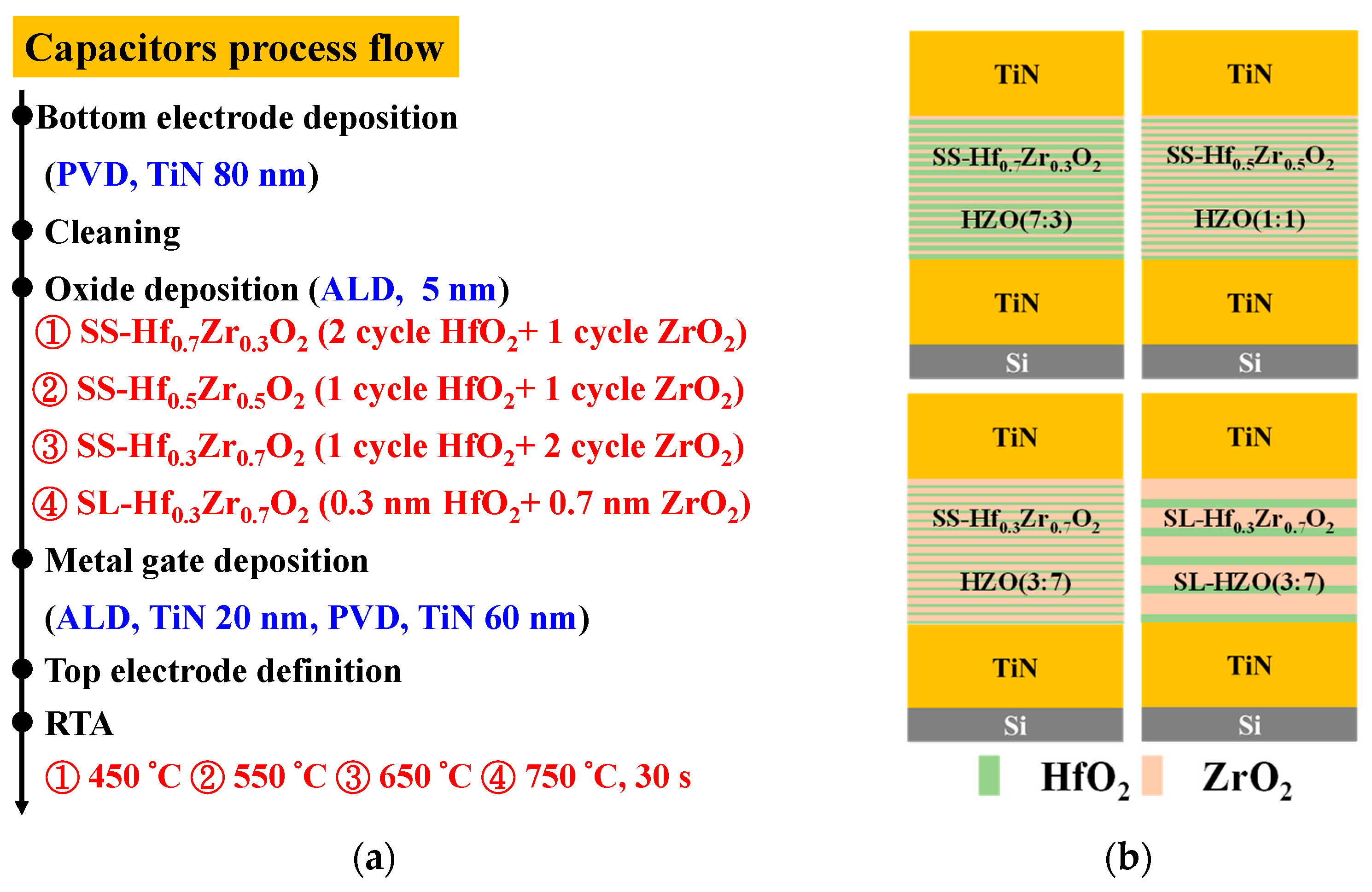
The wafer was transferred to an atomic layer deposition (ALD) chamber, where the native IL underwent NH3 plasma treatment to enhance interface quality and reduce defect formation. This treatment was performed at 250 °C with a power setting of 200 watts for 120 s, utilizing ammonia gas. Subsequently, a 5 nm thick SL-Hf0.3Zr0.7O2 dielectric was deposited via ALD, consisting of alternating 0.3 nm and 0.7 nm layers. The Hf1-xZrxO2 structure was engineered using a cycle-controlled layer-by-layer deposition process to ensure precise composition modulation. Gate metal deposition was then carried out using a combination of ALD and physical vapor deposition (PVD) to ensure full NS gate encapsulation.
The gate pattern was subsequently transferred onto the substrate through EBL and RIE (also with isotropic etching gases Cl2). Following gate formation, the source/drain (S/D) regions were doped with n-type impurities using phosphorus ion implantation at doses of 1 × 1015 cm−2, with implantation energies of 10 keV, 20 keV, and 30 keV to achieve optimized doping profiles. Finally, dielectric crystallization and dopant activation were performed in a nitrogen ambient using rapid thermal annealing (RTA) at 550 °C for 30 s. This systematic fabrication process ensures the realization of high-performance Si NSGAAFET devices with the optimized SL-Hf0.3Zr0.7O2 dielectric, demonstrating its feasibility for advanced CMOS scaling.
Figure 1a illustrates the process flow of capacitor fabrication, while Figure 1b shows the schematic cross-sectional view of the Hf1-xZrxO2 metal-insulator-metal (MIM) capacitors with SS and SL configurations. Figure 2a illustrates the Si NSGAAFETs process flow, while Figure 2b shows the schematic cross-sectional view of the Si NSGAAFET, clearly depicting the structural configuration of the device. Figure 2c presents the transmission electron microscope (TEM) image and energy-dispersive X-ray spectroscopy (EDS) mapping of the Si NSGAAFET. The high-k dielectric layer, consisting of cycle-controlled SS-Hf0.3Zr0.7O2 and SL-Hf0.3Zr0.7O2, features individual layer thicknesses of 0.3 nm for HfO2 and 0.7 nm for ZrO2, resulting in a final stack thickness of nearly 5.13 nm.
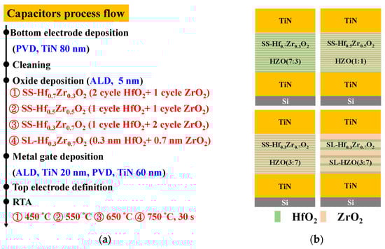
Figure 1.
(a) Fabrication process flow and (b) cross-sectional schematic of Hf1-xZrxO2 MIM capacitors with SS and SL configurations.
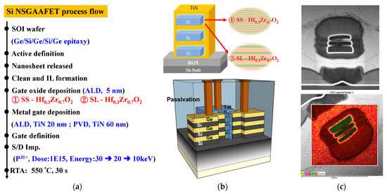
Figure 2.
(a) Process flow and (b) cross-sectional schematic of Si NSGAAFET. (c) TEM image and EDS mapping of Si NSGAAFET, showing devices with a final high-k stack of 5.13 nm and NS structure.
3. Results and Discussion
3.1. Investigation of Composition-Dependent Hafnium Zirconium Oxide Capacitors with Solid Solution and Superlattice Structure
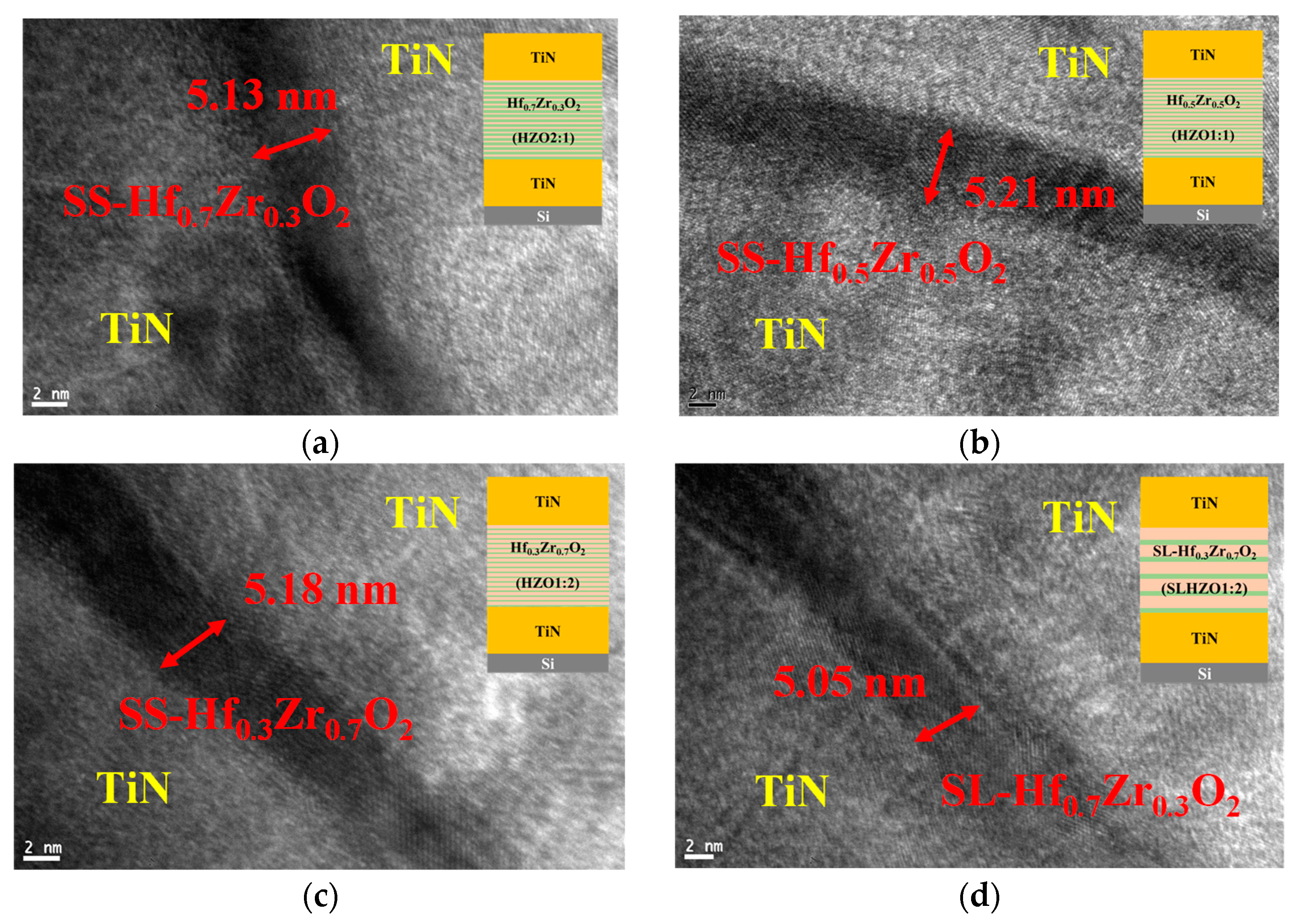
Figure 3a–d show the transmission electron microscope (TEM) images of the four conditions: SS-Hf0.7Zr0.3O2, SS-Hf0.5Zr0.5O2, SS-Hf0.3Zr0.7O2, and SL-Hf0.3Zr0.7O2 MIM capacitors, respectively, had a total thickness of approximately 5 nm. All devices in this study were fabricated and tested alongside control samples to ensure consistency and mitigate potential variations.

Figure 3.
Cross-sectional TEM images of MIM capacitors with approximately 5 nm thick (a) SS-Hf0.7Zr0.3O2; (b) SS-Hf0.5Zr0.5O2; (c) SS-Hf0.3Zr0.7O2; and (d) SL-Hf0.3Zr0.7O2 dielectric layers. The thickness of dielectric layers and materials as shown in the figures.
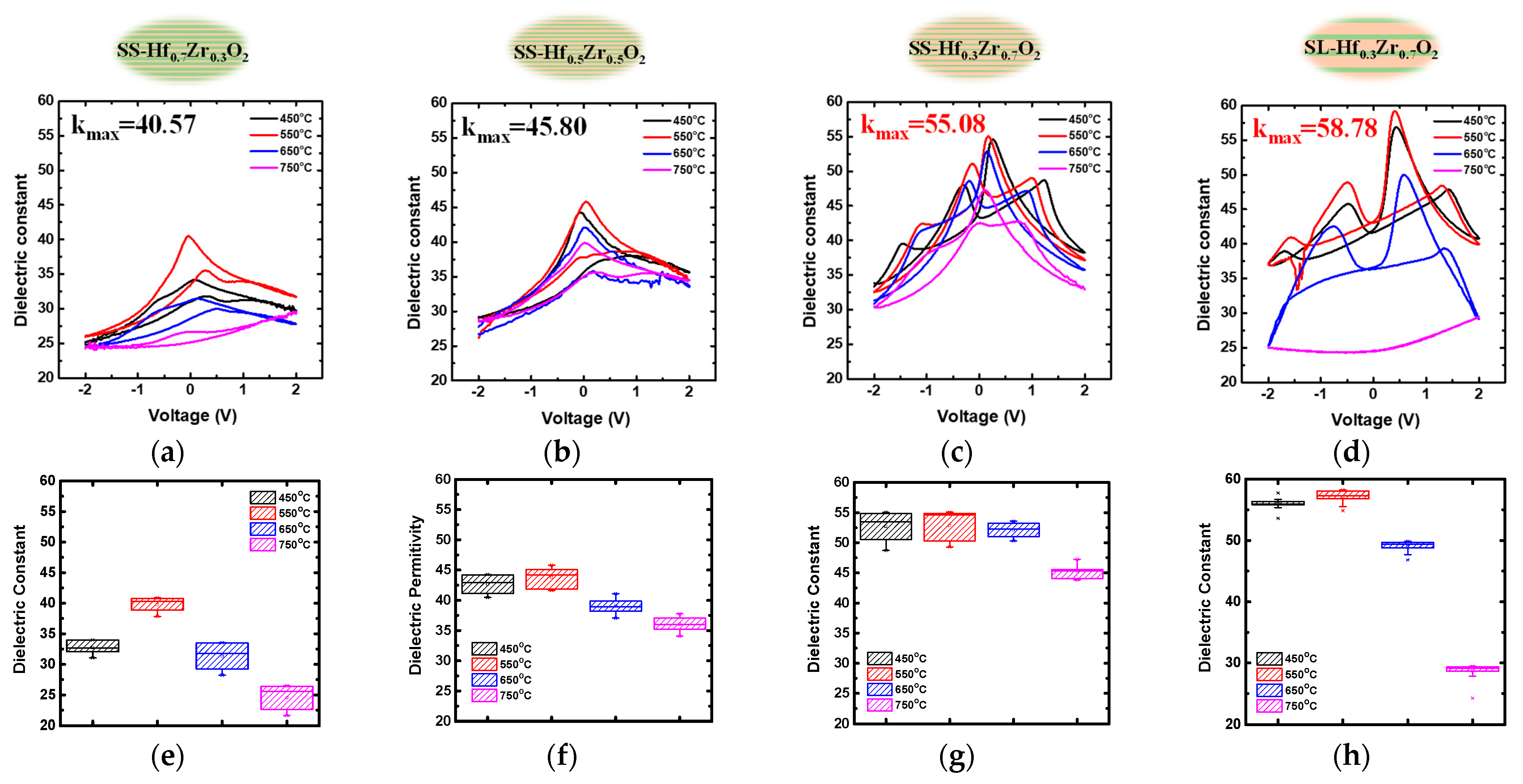
Figure 4a–d present the dielectric constant versus voltage characteristics calculated from the C-V curves of MIM capacitors incorporating Hf1-xZrxO2 dielectrics with both SS and SL structures at different temperatures. The SS-Hf0.7Zr0.3O2 dielectric exhibits behavior similar to conventional HfO2 dielectrics, while SS-Hf0.5Zr0.5O2 demonstrates characteristics typical of ferroelectric materials, with a peak capacitance near 0 V due to dipole polarization. Corresponding box plots of k-values further validate these findings in Figure 4e–h, respectively. The SS-Hf0.3Zr0.7O2 dielectric shows a high k-value of 55 at 550 °C, which is primarily attributed to the morphotropic phase boundary (MPB) effect, where the coexistence of the o-phase and t-phase enhances dielectric performance [18]. As the ZrO2 content increases, the observed shift in the peak k-value with temperature suggests a phase transition between the o-phase and t-phase [19]. This boundary not only improves the dielectric constant but also reduces the hysteresis and leakage current, making SL structures highly suitable for advanced semiconductor devices. Furthermore, the statistical analysis of the phase diagrams shows that the distribution in Figure 4h is denser than that in Figure 4g, confirming that the presence of the MPB enhances the stability of the dielectric layer.
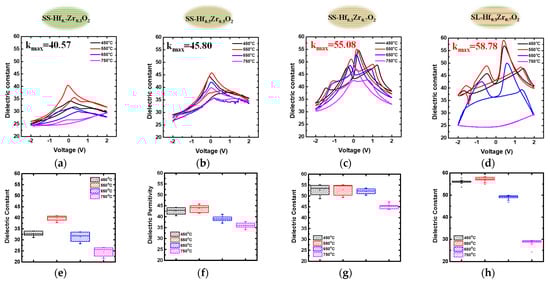
Figure 4.
Temperature-dependent dielectric constant versus voltage characteristics of Hf1-xZrxO2 MIM capacitors: (a–d) k-V curves and (e–h) corresponding k-value distribution box plots for (a,e) SS-Hf0.7Zr0.3O2, (b,f) SS-Hf0.5Zr0.5O2, (c,g) SS-Hf0.3Zr0.7O2, and (d,h) SL-Hf0.3Zr0.7O2. The SL-Hf0.3Zr0.7O2 exhibits an enhanced k-value (~59) at 550 °C due to MPB-induced o-phase and t-phase coexistence.
When utilizing the SL stacking structure, the SL-Hf0.3Zr0.7O2 dielectric achieves a higher k-value of 59 at 550 °C, and the statistical data show a more concentrated and stable distribution. These results indicate that the SL stacking method significantly enhances both the k-value and electrical stability compared to the SS approach. This improvement is attributed to the mechanical stress and changes in free energy at the interfaces, which promote superior electrical performance. However, at high annealing temperatures of 750 °C, there is a significant decrease in both the dielectric constant. The capacitance values markedly decrease, leading to a noticeable reduction in the k-value.
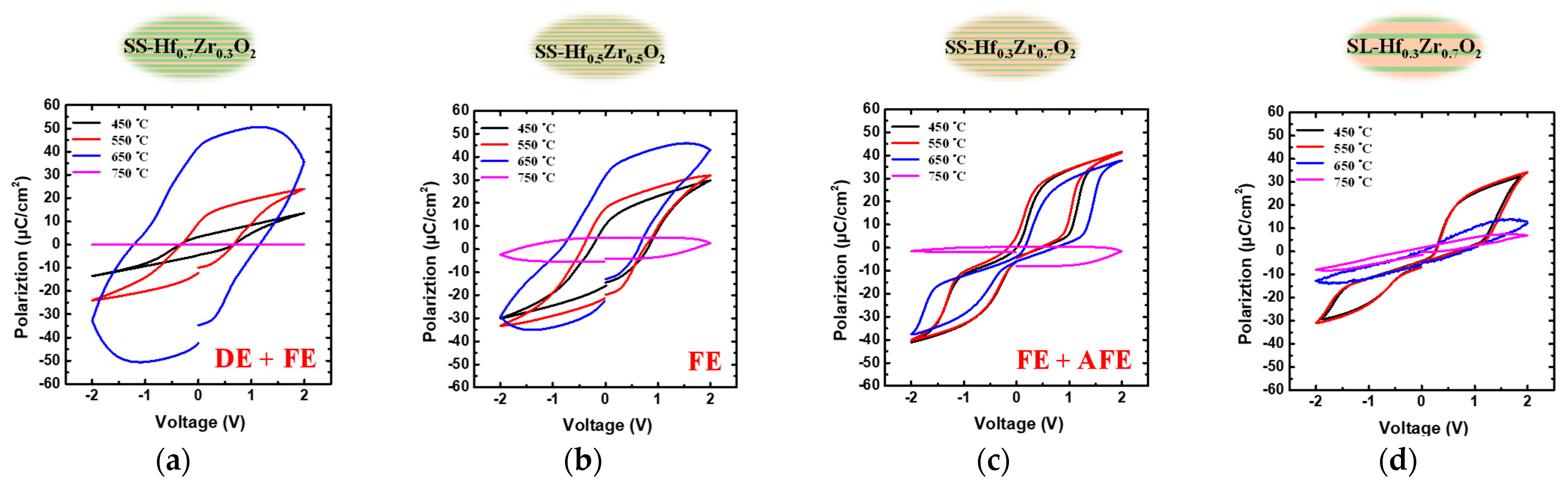
Figure 5a–d present the P-V characteristics of MIM structures incorporating Hf1-xZrxO2 dielectrics at various annealing temperatures. The SS-Hf0.7Zr0.3O2 film demonstrates a combination of dielectric and ferroelectric phases, particularly at 450 °C. The SS-Hf0.7Zr0.3O2 sample exhibits a reduced hysteresis loop with a remanent polarization (2Pr) of approximately 20 µC/cm2. In contrast, the SS-Hf0.5Zr0.5O2 sample displays a typical ferroelectric hysteresis loop with a 2Pr value of around 40 µC/cm2, making it suitable for ferroelectric memory applications. Both the SS-Hf0.3Zr0.7O2 and SL-Hf0.3Zr0.7O2 samples exhibit a combination of ferroelectric and antiferroelectric (AFE) phases, with a 2Pr value of approximately 10 µC/cm2 and 0 µC/cm2 near 0 V. The primary challenge with FE logic devices lies in the internal electric fields generated by dipoles, which lead to hysteresis effects. This hysteresis can cause significant shifts in the VTH, making these devices less suitable for logic applications where precise control over switching is critical. The proposed characteristics of the capacitance can effectively reduce VTH shift, making it suitable for logic device applications. Notably, the SL-Hf0.3Zr0.7O2 dielectric shows minimal leakage current as the temperature increases, indicating the structural stability of this material [20]. The residual polarization decreases significantly at this elevated temperature, indicating that high thermal conditions adversely affect the dielectric properties of the material. These findings further correlate with the peak capacitance observed in Figure 4, where the position of the capacitance peak is attributed to the interplay between the different phases.
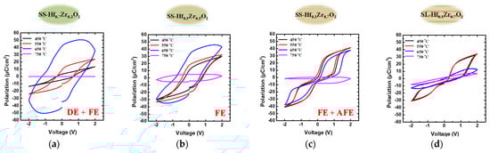
Figure 5.
Temperature-dependent P-V characteristics of Hf1-xZrxO2 MIM capacitors with (a) SS-Hf0.7Zr0.3O2 showing mixed DE/FE phases with 2Pr ~20 µC/cm2; (b) SS-Hf0.5Zr0.5O2 exhibiting ferroelectric behavior with 2Pr ~40 µC/cm2; (c) SS-Hf0.3Zr0.7O2; and (d) SL-Hf0.3Zr0.7O2 demonstrating FE/AFE phase coexistence with 2Pr ~10 µC/cm2 and 0 µC/cm2.
3.2. Comparison and Enhancement of Silicon Nanosheet Gate-All-Around Field-Effect Transistors with Solid Solution and Superlattice Structures
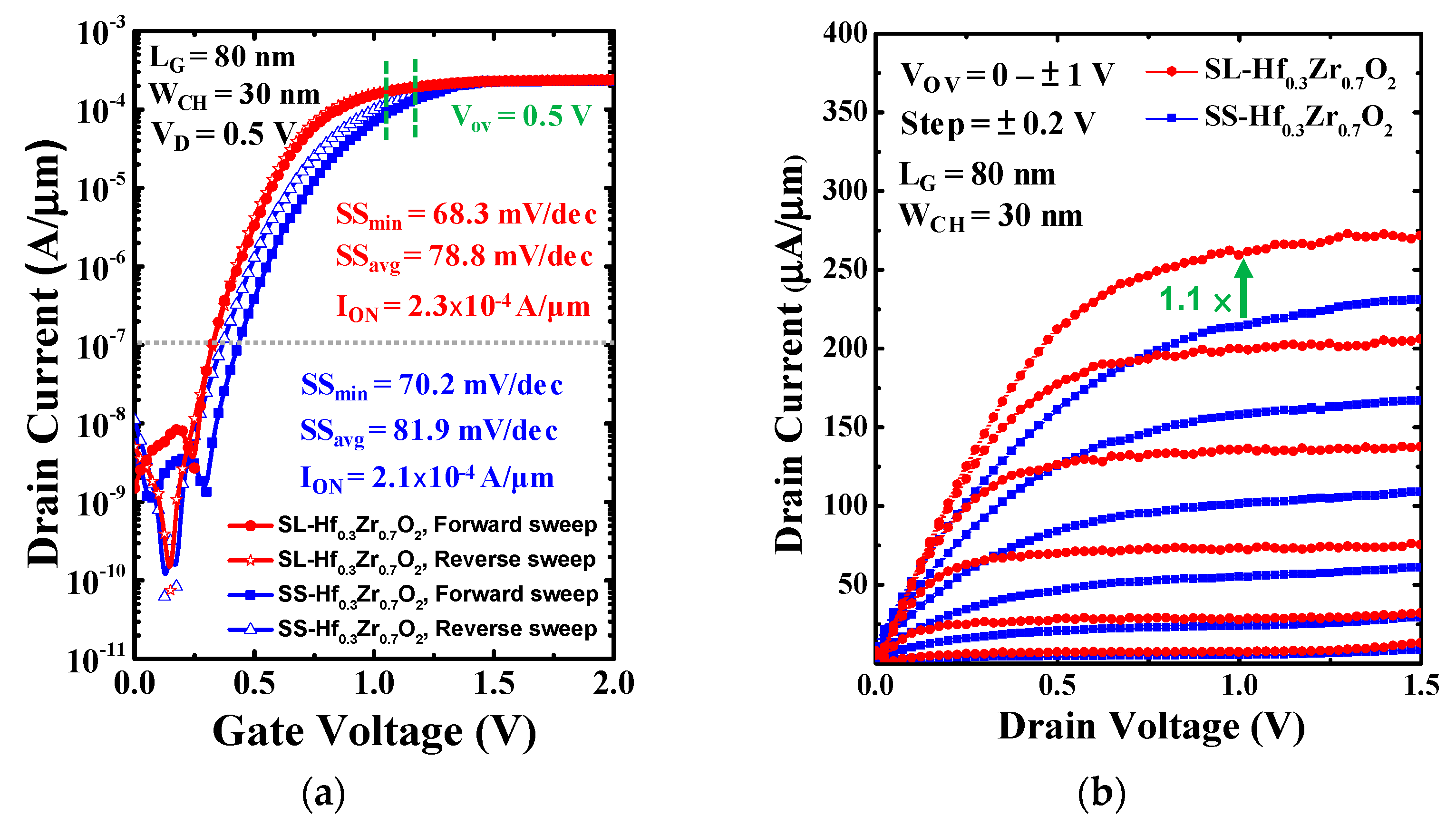
Figure 6a demonstrates the drain current (ID) versus gate voltage (VG), and Figure 6b demonstrates the ID versus drain voltage (VD) characteristics of N-type Si NSGAAFETs incorporating SS-Hf0.3Zr0.7O2 and SL-Hf0.3Zr0.7O2 dielectrics. The device dimensions include a channel width (WCH) of 30 nm and a gate length (LG) of 80 nm. Both forward (solid line) and reverse (dashed line) sweeps are shown, confirming minimal hysteresis. Compared to the SS-Hf0.3Zr0.7O2 dielectric, the SL structure significantly reduces hysteresis while maintaining a higher ION. Specifically, the SS-Hf0.3Zr0.7O2 sample exhibits an average subthreshold swing (SSavg = 81.9 mV/dec), a minimum subthreshold swing (SSmin = 70.2 mV/dec), and ION of 2.1 × 10⁻⁴. In contrast, the SL-Hf0.3Zr0.7O2 sample shows an average subthreshold swing (SSavg = 78.8 mV/dec), minimum subthreshold swing (SSmin = 68.3 mV/dec), and ION of 2.3 × 10⁻⁴, further confirming the enhanced performance. However, the off-current reached a relatively large value of 10−9 A/µm at VG = 0 and VD = 0.5 V. This significant off-current may be attributed to poor interface quality, which can lead to enhanced leakage effects. Defects at the interface can create additional pathways for current flow, resulting in increased off-current levels in the device. The normalized ID, divided by the footprint width and VTH, was determined at a constant ID of 10−7 A/µm.

Figure 6.
(a) ID-VG and (b) ID-VD characteristics of N-type Si NSGAAFETs (WCH = 30 nm, LG = 80 nm) with SS and SL-Hf0.3Zr0.7O2 forward (solid) and reverse (dashed) sweeps. The SL structure exhibits improved performance compared to the SS structure.
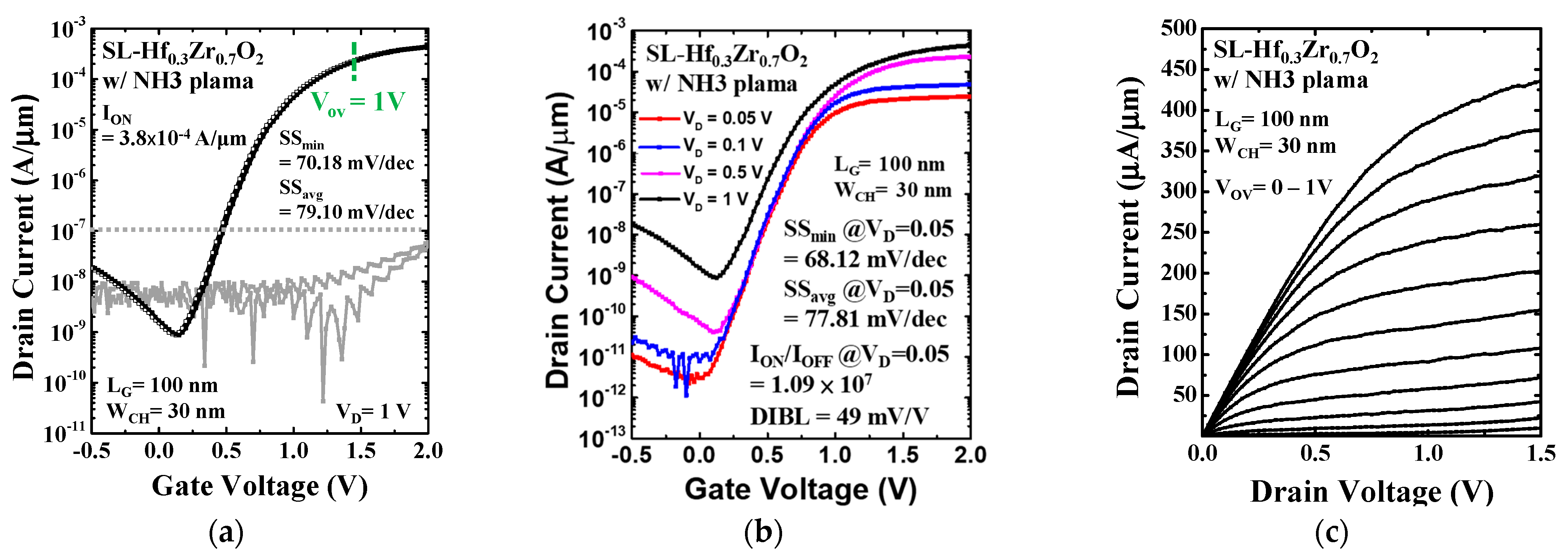
To further suppress IOFF in NMOS devices, NH3 plasma treatment was employed to enhance the quality of the IL. As shown in Figure 7a, the electrical characteristics of devices treated with NH3 plasma show that SSavg = 79.10 mV/dec and SSmin = 70.18 mV/dec with an ION of 3.8 × 10⁻⁴ and the gate leakage current (IG) (shown by the gray curve). Figure 7b shows an improvement in IOFF (shown by a purple curve) and showcases leakage currents as low as 10−10A/μm at VG = 0 and VD = 0.5 V. An ION/IOFF of up to 107, SSavg = 77.81 mV/dec, SSmin = 68.12 mV/dec, and drain-induced barrier-lowering (DIBL = 49 mV/V) at VD = 0.5 V alongside the ID-VD characteristics are demonstrated in Figure 7c. This enhancement underscores the effectiveness of NH3 plasma treatment in improving the electrical performance of the devices, making this approach highly compatible with CMOS technology platforms.
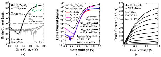
Figure 7.
(a) ID-VG characteristics of the SL-Hf0.3Zr0.7O2 dielectric applied on N-type Si NSGAAFETs with NH3 plasma treatment showing reduced IG and high ION. (b) ID-VG characteristics with different drain voltage levels, exhibiting enhanced ION/IOFF ratios (~107) with (c) corresponding ID-VD curves.
Table 1 highlights the performance metrics in comparison with other contemporary devices reported in the literature. Key parameters such as on-off current ratios, subthreshold slopes, and overall device stability are systematically compared. This approach allows for a clearer understanding of the proposed device standards relative to existing technologies.

Table 1.
Comparison with other contemporary devices.
4. Conclusions
This study introduces an optimized SL-Hf0.3Zr0.7O2 dielectric for Si NSGAAFETS, demonstrating its potential to address challenges associated with CMOS scaling and advanced logic applications. The dielectric properties of Hf1-xZrxO2 with SS and SL structures were systematically investigated and compared through C-V and P-V measurements under various annealing conditions. The optimized composition achieved a high dielectric constant of 59, leading to a significant reduction in EOT. When integrated into Si NSGAAFETs, the SL dielectric combined this with the NH3 plasma treatment of the IL and exhibited superior electrical performance, including a higher ION/IOFF, enhanced drive current, and notably reduced leakage current. These results validate the effectiveness of the SL-Hf0.3Zr0.7O2 dielectric in enhancing the performance of next-generation logic devices.
Author Contributions
Conceptualization and methodology, Y.-J.Y., G.-L.L., F.-J.H., Y.-S.L. and Y.-C.W.; investigation, Y.-J.Y., Y.-M.F. and Y.-H.C.; writing—original draft preparation, Y.-J.Y.; writing—review and editing, Y.-J.Y., C.-Y.W. and K.-T.H.; supervision, Y.-C.W. All authors have read and agreed to the published version of the manuscript.
Funding
This research was financially supported in part by the National Science and Technology Council with grant number NSTC 112-2221-E-007-110-MY3, NSTC 113-2119-M-007-014-MBK, NSTC 113-2218-E-A49-021-MBK and NSTC 113-2221-E-492-008-MBK.
Institutional Review Board Statement
Not applicable.
Informed Consent Statement
Not applicable.
Data Availability Statement
The data presented in this study are available on request from the corresponding author.
Acknowledgments
The authors are grateful for the support of the Taiwan Semiconductor Research Institute (TSRI), the National Yang Ming Chiao Tung University Nano Facility Center (NFC) and United Microelectronics Corporation (UMC) Fellowship, Taiwan.
Conflicts of Interest
The authors declare no conflicts of interest.
References
- Kuhn, K.J.; Murthy, A.; Kotlyar, R.; Kuhn, M. (Invited) Past, Present and Future: SiGe and CMOS Transistor Scaling. ECS Trans. 2010, 33, 3. [Google Scholar] [CrossRef]
- Ando, T. Ultimate Scaling of High-κ Gate Dielectrics: Higher-κ or Interfacial Layer Scavenging? Materials 2012, 5, 478–500. [Google Scholar] [CrossRef] [PubMed]
- Si, M.; Lin, Z.; Chen, Z.; Sun, X.; Wang, H.; Ye, P.D. Scaled indium oxide transistors fabricated using atomic layer deposition. Nat. Electron. 2022, 5, 164–170. [Google Scholar] [CrossRef]
- Ni, K.; Saha, A.; Chakraborty, W.; Ye, H.; Grisafe, B.; Smith, J.; Rayner, G.B.; Gupta, S.; Datta, S. In Equivalent Oxide Thickness (EOT) Scaling With Hafnium Zirconium Oxide High-κ Dielectric Near Morphotropic Phase Boundary. In Proceedings of the 2019 IEEE International Electron Devices Meeting (IEDM), San Francisco, CA, USA, 7–11 December 2019; pp. 7.4.1–7.4.4. [Google Scholar] [CrossRef]
- Chakraborty, W.; Jose, M.S.; Gomez, J.; Saha, A.; Aabrar, K.A.; Fay, P.; Gupta, S.; Datta, S. In Higher-k Zirconium Doped Hafnium Oxide (HZO) Trigate Transistors with Higher DC and RF Performance and Improved Reliability. In Proceedings of the 2021 Symposium on VLSI Technology, Kyoto, Japan, 13–19 June 2021; pp. 1–2. [Google Scholar]
- Wong, H.; Iwai, H. On the scaling of subnanometer EOT gate dielectrics for ultimate nano CMOS technology. Microelectron. Eng. 2015, 138, 57–76. [Google Scholar] [CrossRef]
- Weng, Z.; Zhao, L.; Lee, C.; Zhao, Y. Phase Transitions and Anti-Ferroelectric Behaviors in Hf1-xZrxO2 Films. IEEE Electron. Device Lett. 2023, 44, 1780–1783. [Google Scholar] [CrossRef]
- Müller, J.; Böscke, T.S.; Schröder, U.; Mueller, S.; Bräuhaus, D.; Böttger, U.; Frey, L.; Mikolajick, T. Ferroelectricity in Simple Binary ZrO2 and HfO2. Nano Lett. 2012, 12, 4318–4323. [Google Scholar] [CrossRef] [PubMed]
- Park, M.H.; Hwang, C.S. Fluorite-structure antiferroelectrics. Rep. Prog. Phys. 2019, 82, 124502. [Google Scholar] [CrossRef] [PubMed]
- Ali, T.; Polakowski, P.; Riedel, S.; Büttner, T.; Kämpfe, T.; Rudolph, M.; Pätzold, B.; Seidel, K.; Löhr, D.; Hoffmann, R.; et al. Silicon doped hafnium oxide (HSO) and hafnium zirconium oxide (HZO) based FeFET: A material relation to device physics. Appl. Phys. Lett. 2018, 112. [Google Scholar] [CrossRef]
- Ferrari, S.; Scarel, G. Oxygen diffusion in atomic layer deposited ZrO2 and HfO2 thin films on Si (100). J. Appl. Phys. 2004, 96, 144–149. [Google Scholar] [CrossRef]
- Gong, Z.; Chen, J.; Peng, Y.; Liu, Y.; Yu, X.; Han, G. Physical origin of the endurance improvement for HfO2-ZrO2 superlattice ferroelectric film. Appl. Phys. Lett. 2022, 121, 242901. [Google Scholar] [CrossRef]
- Park, M.H.; Kim, H.J.; Lee, G.; Park, J.; Lee, Y.H.; Kim, Y.J.; Moon, T.; Kim, K.D.; Hyun, S.D.; Park, H.W.; et al. A comprehensive study on the mechanism of ferroelectric phase formation in hafnia-zirconia nanolaminates and superlattices. Appl. Phys. Rev. 2019, 6, 041403. [Google Scholar] [CrossRef]
- Liang, Y.K.; Li, W.L.; Wang, Y.J.; Peng, L.C.; Lu, C.C.; Huang, H.Y.; Yeong, S.H.; Lin, Y.M.; Chu, Y.H.; Chang, E.Y.; et al. ZrO2-HfO2 Superlattice Ferroelectric Capacitors with Optimized Annealing to Achieve Extremely High Polarization Stability. IEEE Electron. Device Lett. 2022, 43, 1451–1454. [Google Scholar] [CrossRef]
- Cheema, S.S.; Shanker, N.; Wang, L.-C.; Hsu, C.-H.; Hsu, S.-L.; Liao, Y.-H.; San Jose, M.; Gomez, J.; Chakraborty, W.; Li, W.; et al. Ultrathin ferroic HfO2–ZrO2 superlattice gate stack for advanced transistors. Nature 2022, 604, 65–71. [Google Scholar] [CrossRef] [PubMed]
- Oh, S.; Jang, H.; Hwang, H. Accurate Evaluation of High-k HZO/ZrO2 Films by Morphotropic Phase Boundary. IEEE Electron. Device Lett. 2024, 45, 28–31. [Google Scholar] [CrossRef]
- Saha, A.K.; Grisafe, B.; Datta, S.; Gupta, S.K. In Microscopic Crystal Phase Inspired Modeling of Zr Concentration Effects in Hf1-xZrxO2 Thin Films. In Proceedings of the 2019 Symposium on VLSI Technology, Kyoto, Japan, 9–14 June 2019; pp. T226–T227. [Google Scholar] [CrossRef]
- Das, D.; Buyantogtokh, B.; Gaddam, V.; Jeon, S. Sub 5 Å-EOT HfₓZr1–xO₂ for Next-Generation DRAM Capacitors Using Morphotropic Phase Boundary and High-Pressure (200 atm) Annealing with Rapid Cooling Process. IEEE Trans. Electron. Devices 2022, 69, 103–108. [Google Scholar] [CrossRef]
- Lehninger, D.; Prabhu, A.; Sünbül, A.; Ali, T.; Schöne, F.; Kämpfe, T.; Biedermann, K.; Roy, L.; Seidel, K.; Lederer, M.; et al. Ferroelectric [HfO2/ZrO2] Superlattices with Enhanced Polarization, Tailored Coercive Field, and Improved High Temperature Reliability. Adv. Phys. Res. 2023, 2, 2200108. [Google Scholar] [CrossRef]
- Huang, C.-Y.; Dewey, G.; Mannebach, E.; Phan, A.; Morrow, P.; Rachmady, W.; Tung, I.-C.; Thomas, N.; Alaan, U.; Paul, R.; et al. 3-D Self-aligned Stacked NMOS-on-PMOS Nanoribbon Transistors for Continued Moore’s Law Scaling. In Proceedings of the 2020 IEEE International Electron Devices Meeting (IEDM), San Francisco, CA, USA, 12–18 December 2020; pp. 20.6.1–20.6.4. [Google Scholar] [CrossRef]
- Jagannathan, H.; Anderson, B.; Sohn, C.-W.; Tsutsui, G.; Strane, J.; Xie, R.; Fan, S.; Kim, K.-I.; Song, S.; Sieg, S.; et al. Vertical-Transport Nanosheet Technology for CMOS Scaling beyond Lateral-Transport Devices. In Proceedings of the 2021 IEEE International Electron Devices Meeting (IEDM), San Francisco, CA, USA, 11–15 December 2021; pp. 26.1.1–26.1.4. [Google Scholar] [CrossRef]
- Mertens, H.; Ritzenthaler, R.; Chasin, A.; Schram, T.; Kunnen, E.; Hikavyy, A.; Ragnarsson, L.-Å.; Dekkers, H.; Hopf, T.; Wostyn, K.; et al. Vertically stacked gate-all-around Si nanowire CMOS transistors with dual work function metal gates. In Proceedings of the 2016 IEEE International Electron Devices Meeting (IEDM), San Francisco, CA, USA, 3–7 December 2016; pp. 19.7.1–19.7.4. [Google Scholar] [CrossRef]

Disclaimer/Publisher’s Note: The statements, opinions and data contained in all publications are solely those of the individual author(s) and contributor(s) and not of MDPI and/or the editor(s). MDPI and/or the editor(s) disclaim responsibility for any injury to people or property resulting from any ideas, methods, instructions or products referred to in the content. |
© 2025 by the authors. Licensee MDPI, Basel, Switzerland. This article is an open access article distributed under the terms and conditions of the Creative Commons Attribution (CC BY) license (https://creativecommons.org/licenses/by/4.0/).