2.3.1. Cation Doping in Polycrystalline In3.9M0.1Se2.95
In the crystal structure of In
4Se
3, the average charge of indium within the layer (In1, In2, and In3 site) is ~1.67+ while that of indium between the layers (In4 site) is 1+. In the solid state chemistry point of view, the carrier concentration in In
4Se
3 based materials could be controlled through replacing the indium by other metals because of their different valence states. It is likely that the In4 site replacement is more susceptible than the other indium site replacements because of strong covalent-ionic interaction between indium at In1, In2, and In3 sites and selenium within the layer. A formation energy calculation using the density functional theory (DFT) was carried out in order to predict the most preferential indium site among In1, In2, In3, and In4 sites for each substituted metal atom we studied here. The formation energies of In
4−xM
xSe
3 (
x = 0.25) were calculated at each possible indium site as follows:
where
Ef is the formation energy and
Et the total energy of each material.
The formation energies of In
4−xMxSe
3 (
x = 0.25) at each indium site are tabulated in
Table 2. This shows that the metal substitution at the In4 site is energetically most favorable for M = Na, Ca, and Pb while other sites are most preferable for M = Sn (In2 site) and M = Zn and Ga (In3 site). In
Figure 10, the crystal structure of In
3.9Zn
0.1Se
2.95 was refined by a full profile Rietveld refinement technique using an LHPM-Rietica program. It can be estimated from the refinement result that the major phase (>97 wt%) is the 4:3 In–Se phase and the minor phase is the 1:1 In–Se phase (<3 wt%). Regarding the metallic radii of the elements (Na, Ca, Zn, Ga, Sn, Pb) studied here, compared to the metallic radius of 1.58 Å for indium, the largest and smallest radius are 1.97 Å for Ca and 1.36 Å for Zn, respectively. A certain amount of metal substitution for indium in the 4:3 indium selenide should affect the variation of the lattice parameters. However, the lattice parameters of In
4−xM
xSe
2.95 samples are fairly similar to each other. Also, these are almost same as that of In
4Se
2.95 (
a = 15.281(1) Å,
b = 12.301(1) Å,
c = 4.075(1) Å). This indicates that the small amount of metal doping below 2.5 at.% for indium on In
4Se
2.95 shows a negligible influence on the lattice parameters.
Table 2.
Formation energies in eV at each indium site for In4−xMxSe3 (x = 0.25).
Table 2.
Formation energies in eV at each indium site for In4−xMxSe3 (x = 0.25).
| In-sites | Na | Ca | Zn | Ga | Sn | Pb |
|---|
| In1 | −0.430 | −1.913 | 0.065 | −0.423 | 0.157 | 0.173 |
| In2 | −0.776 | −1.831 | 0.215 | −0.422 | 0.022 | 0.065 |
| In3 | −0.527 | −1.913 | 0.011 | −0.518 | 0.139 | 0.234 |
| In4 | −1.716 | −2.618 | 0.246 | −0.243 | 0.056 | −0.144 |
Figure 10.
The observed (dots) and calculated (line) powder diffraction patterns of polycrystalline In3.9Zn0.1Se2.95 after the completion of Rietveld refinements. The upper sets of vertical bars located just below the plots of the observed and calculated intensities indicate the calculated positions of the Bragg peaks of the majority 4:3 In–Se phase, while the lower sets of bars correspond to the calculated positions of the Bragg peaks of the 1:1 In–Se impurity. The difference, Yobs – Ycalc, is shown at the bottom of the plot.
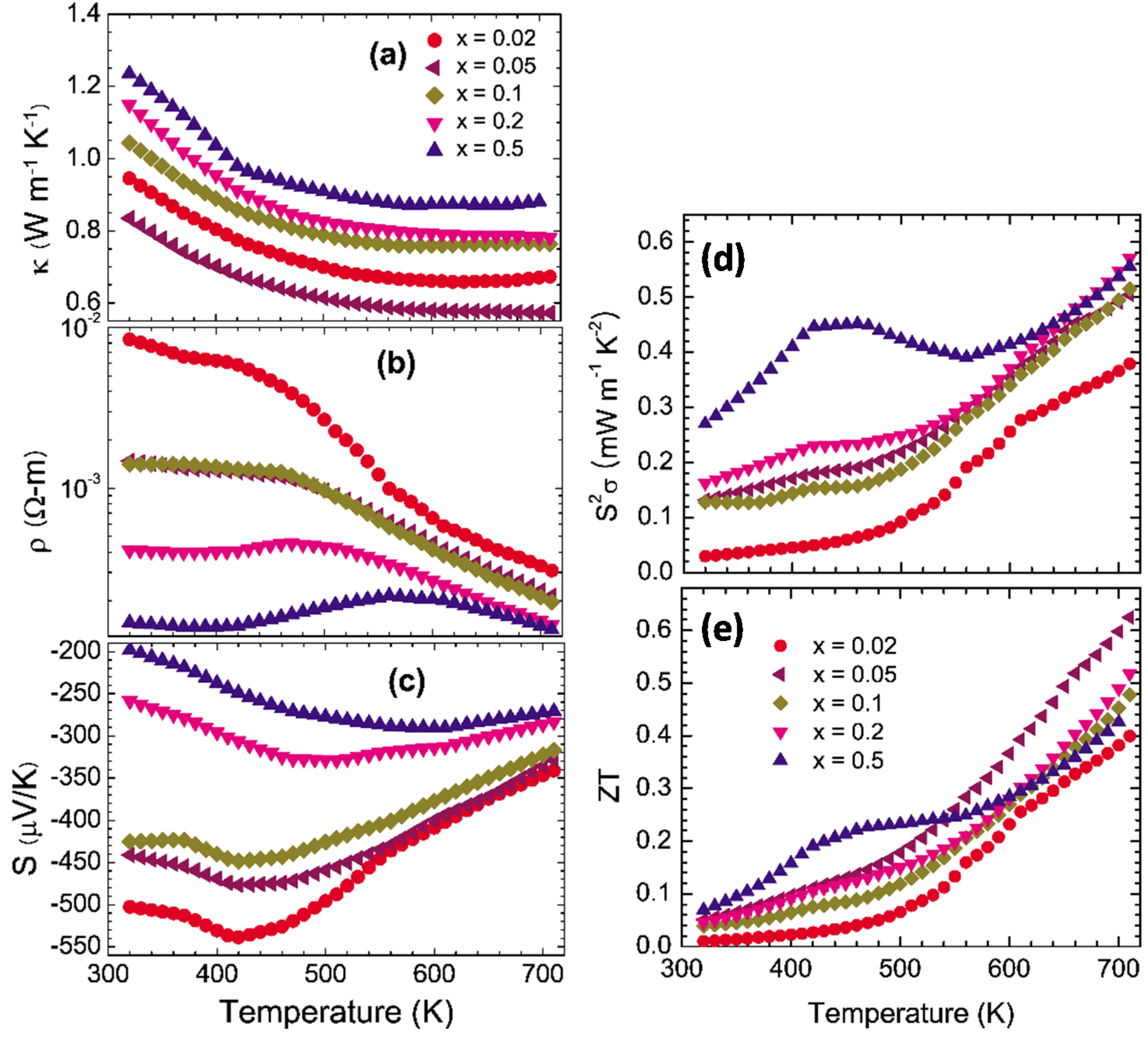
The thermoelectric properties of polycrystalline In
3.9M
0.1Se
2.95 (M = Na, Ca, Zn, Ga, Sn, Pb) samples were investigated in order to explore the effect of cationic (metallic) substitution on thermoelectric performance of In
4Se
2.95 [
21] which was reported to the optimal Se-deficient composition for a high
ZT among In
4Se
3-x polycrystalline materials.
Figure 11a shows the electrical conductivity σ as a function of temperature for polycrystalline In
3.9M0.1Se
2.95 (M = Na, Ca, Zn, Ga, Sn, Pb) and In
4Se
2.95 samples. Compared to the electrical conductivity at ~320 K of ~7 S/cm for In
4Se
2.95, those at ~320 K for In
3.9Na
0.1Se
2.95, In
3.9Ca
0.1Se
2.95, In
3.9Zn
0.1Se
2.95, In
3.9Ga
0.1Se
2.95, In
3.9Sn
0.1Se
2.95, and In
3.9Pb
0.1Se
2.95 are ~33, ~95, ~0.5, ~4, ~1, and ~37 S/cm, respectively. The Hall mobility μ
H can be expressed as
, where σ is the electrical conductivity,
nH the Hall carrier concentration, and
e the electron charge.
The Hall carrier concentrations of In
3.9M
0.1Se
2.95 polycrystalline samples are measured at room temperature (
Table 3). Thus, compared to the room temperature Hall mobility of ~242.7 cm
2/V·s for In
4Se
2.95, those for In
3.9Na
0.1Se
2.95, In
3.9Ca
0.1Se
2.95, In
3.9Zn
0.1Se
2.95, In
3.9Ga
0.1Se
2.95, In
3.9Sn
0.1Se
2.95, and In
3.9Pb
0.1Se
2.95 are ~17.2, ~6.8, ~36.8, ~45.5, ~8.3, and ~45.3 cm
2/V·s, respectively (
Table 3). For most of our samples the electrical conductivities increase with increasing temperature indicative of semiconducting behavior. However, the sample of In
3.9Na
0.1Se
2.95 and In
3.9Ca
0.1Se
2.95 show metal-semiconductor-like transitions at ~470 K, which probably comes from a thermal stability issue (
i.e., decomposition of the compounds at a certain temperature). Compared to ~43 S/cm at ~700 K for In
4Se
2.95, the respective electrical conductivities at ~700 K for M = Na, Ca, Zn, Ga, Sn, and Pb are ~70, ~102, ~40, ~39, ~40, and ~77 S/cm. Especially, it is noted that the electrical conductivity at ~320 K for In
3.9Ca
0.1Se
2.95 is ~15 times higher than In
4Se
2.95 indicating that the Ca substitution should be effective for increasing the carrier concentration. This is supported by the room temperature electron concentration of 8.7 × 10
19 cm
−3 for In
3.9Ca
0.1Se
2.95 compared to that of 1.74 × 10
17 cm
−3 for In
4Se
2.95 (
Table 3). The most preferential site for metal substitution in the In
3.9M
0.1Se
2.95 compounds (
Table 2) may be associated with the carrier concentration. The Na, Ca, and Pb substituted compounds show much higher room temperature electron concentrations than the Zn, Ga, and Sn substituted ones. This implies that metal substitutions at the In4 site are more effective to increase the carrier concentration than those at other indium sites.
Figure 11.
Temperature dependence of (
a) electrical conductivity, (
b) Seebeck coefficient, (
c) power factor, and (
d) calculated Seebeck coefficient by Boltzmann transport equation of polycrystalline samples of In
3.9M
0.1Se
2.95 (M = Na, Ca, Zn, Ga, Sn, Pb) and In
4Se
2.95. Reproduced with permission from AIP Publishing LLC, 2011 [
27].
Table 3.
Room temperature carrier concentrations and Hall mobilities of the polycrystalline samples of In3.9M0.1Se2.95 (M = Na, Ca, Zn, Ga, Sn, Pb) and In4Se2.95.
Table 3.
Room temperature carrier concentrations and Hall mobilities of the polycrystalline samples of In3.9M0.1Se2.95 (M = Na, Ca, Zn, Ga, Sn, Pb) and In4Se2.95.
| Composition | Electron Concentration (cm−3) | Hall Mobility (cm2/V s) |
|---|
| In4Se2.95 | 1.7 × 10¹⁷ | 242.7 |
| In3.9Na0.1Se2.95 | 1.2 × 10¹⁹ | 17.2 |
| In3.9Ca0.1Se2.95 | 8.7 × 10¹⁹ | 6.8 |
| In3.9Zn0.1Se2.95 | 8.5 × 10¹⁶ | 36.8 |
| In3.9Ga0.1Se2.95 | 5.5 × 10¹⁷ | 45.5 |
| In3.9Sn0.1Se2.95 | 7.5 × 10¹⁷ | 8.3 |
| In3.9Pb0.1Se2.95 | 5.1 × 10¹⁸ | 45.3 |
Figure 11b shows the temperature dependent Seebeck coefficient
S of the polycrystalline samples of In
3.9M
0.1Se
2.95 (M = Na, Ca, Zn, Ga, Sn, Pb) and In
4Se
2.95. All samples exhibit negative values of Seebeck coefficient indicating the electron as a major charge carrier. In particular, the samples of In
3.9Na
0.1Se
2.95 and In
3.9Ca
0.1Se
2.95 exhibit significantly lower absolute values of Seebeck coefficient over the measured temperature range compared to In
4Se
2.95. For instance, the absolute value of Seebeck coefficient at ~320 K for In
3.9Ca
0.1Se
2.95 is ~1/22 times smaller than In
4Se
2.95 when its electrical conductivity at the same temperature is ~15 times higher than In
4Se
2.95. We can expect that the calcium substitution on In
4Se
2.95 should lower its power factor. For degenerate semiconductors the Seebeck coefficient is inversely proportional to the carrier concentration according to the below equation [
22]:
where
kB is the Boltzmann constant,
e the electron charge,
h the Planck constant,
md* the effective mass, and
n the carrier concentration.
We utilized a Boltzmann transport equation (BTE) using a rigid band approximation in order to calculate the Seebeck coefficient as a function of temperature at the experimentally measured each carrier concentration of the polycrystalline samples of In
3.9M
0.1Se
2.95. In this calculation, the band gap of 0.4 eV was taken into account because of the empirical band gap of ~0.4 eV for polycrystalline In
4Se
2.95 according to the equation
Eg = 2
e│
Smax│
Tmax where
Eg is the band gap,
e the electron charge, │
Smax│ the maximum absolute value of Seebeck coefficient, and
Tmax the temperature at which the maximum occurs (
i.e., │
Smax│~ 480 μV/K and
Tmax ~ 420 K for polycrystalline In
4Se
2.95). The calculated temperature dependent Seebeck coefficients of In
3.9M
0.1Se
2.95 compounds using BTE are shown in
Figure 11d. It is noted that for each sample the temperature dependence of Seebeck coefficient by BTE are nearly similar to those by experimental measurement. Thus, this strongly indicates that the cationic (metallic) substitution on In
4Se
2.95 decreases (or increases) its Seebeck coefficient in absolute magnitude with increasing (or decreasing) the electron concentration because of the substituted metals located at indium sites in light of the formation energy calculation results and their role on the control of carrier concentration. The quantum confinement effect of quasi-one-dimensional chains on the Seebeck coefficient for the 4:3 indium selenide may not be either somewhat weakened or lost by the metal substitutions for indium sites in the lattice of the 4:3 indium selenide.
The corresponding temperature dependent power factors σ
S2 of the polycrystalline samples of In
3.9M
0.1Se
2.95 (M = Na, Ca, Zn, Ga, Sn, Pb) and In
4Se
2.95 are plotted in
Figure 11c. For all samples the power factor increases with increasing temperature, which is similar to In
4Se
2.95. As expected, all the samples show lower power factors than ~1.3 μW/cm·K
2 at ~320 K for polycrystalline In
4Se
2.95. It is noted that the cationic (metallic) replacement on In
4Se
2.95 lowers its power factor due to the larger reduction on the absolute value of Seebeck coefficient with the smaller increase in the electrical conductivity.
Figure 12a shows the thermal conductivity κ as a function of temperature for the polycrystalline samples of In
3.9M
0.1Se
2.95 (M = Na, Ca, Zn, Ga, Sn, Pb) and In
4Se
2.95. The thermal conductivities of In
3.9M
0.1Se
2.95 are higher than that of In
4Se
2.95 over the measured temperature range. Normally, the thermal conductivity is the sum of the electronic thermal conductivity κ
elec and the lattice thermal conductivity κ
latt. The κ
elec can be calculated from the Wiedemann-Franz law, κ
elec =
Lσ
T, where
L is the Lorenz number. Subtracting the electronic term from the total thermal conductivity one obtains an estimate of the lattice thermal conductivity of a sample. However, for all the samples in this work their lattice thermal conductivities are approximately same as their total thermal conductivities because their electronic thermal conductivities are quite low (
i.e., for In
3.9Na
0.1Se
2.95 the electronic thermal conductivity κ
elec at ~320 K is ~0.03 W/m·K when we take the Lorenz number
L as 2.45 × 10
−8 V
2/K
2 for metals). It is noted that the room temperature lattice thermal conductivity of In
4Se
2.95 is comparable to that of nanostructured bulk thermoelectric materials such as Ag
1−xPb
18SbTe
20 and Bi
xSb
2−xTe
3 (
i.e., ~0.8 W/m·K for Ag
1−xPb
18SbTe
20 and ~0.6 W/m·K for Bi
xSb
2−xTe
3) [
25,
28].
Figure 12.
(
a) Temperature dependence of thermal conductivity, and (
b) the thermoelectric figure of merit of polycrystalline samples of In
3.9M
0.1Se
2.95 (M = Na, Ca, Zn, Ga, Sn, Pb) and In
4Se
2.95. Reproduced with permission from AIP Publishing LLC, 2011 [
27].
Figure 12.
(
a) Temperature dependence of thermal conductivity, and (
b) the thermoelectric figure of merit of polycrystalline samples of In
3.9M
0.1Se
2.95 (M = Na, Ca, Zn, Ga, Sn, Pb) and In
4Se
2.95. Reproduced with permission from AIP Publishing LLC, 2011 [
27].
In general, the alloying/solid solution (point defect scattering) in a compound should decrease its lattice thermal conductivity further compared to the compound having no point defect. However, in the case of the 4:3 indium selenide, the point defects do not reduce the lattice thermal conductivities further compared to that of polycrystalline In
4Se
2.95, and those of In
3.9M
0.1Se
2.95 are rather higher than that of In
4Se
2.95. The reasons should be as follows: the 4:3 indium selenide is a charge density wave system in which a strong electron-phonon coupling breaks the translational symmetry of lattice (
i.e., Peierls distortion) [
7,
15]. We speculate that the cationic (metallic) substitution on the bulk low-dimensional layered In
4Se
3−x crystal either significantly weakens or removes the effect of the Peierls distortion on the reduction in lattice thermal conductivity probably due to the metal substitution at the indium sites. Thus, the main reduction in the lattice thermal conductivity of polycrystalline In
4−xMxSe
2.95 does not result from the Peierls distortion while the lattice thermal conductivity of In
4Se
2.95 is quite suppressed mainly by the Peierls distortion. This can explain why the point defects do not further reduce the lattice thermal conductivity of In
4Se
2.95.
Finally, the dimensionless thermoelectric figure of merit
ZTs for the polycrystalline samples of In
3.9M
0.1Se
2.95 (M = Na, Ca, Zn, Ga, Sn, Pb) and In
4Se
2.95 are plotted in
Figure 11b. For all samples, the
ZT increases with increasing temperature. Compared to the
ZT of ~0.05 at ~320 K for In
4Se
2.95, those at ~320 K for In
3.9Na
0.1Se
2.95, In
3.9Ca
0.1Se
2.95, In
3.9Zn
0.1Se
2.95, In
3.9Ga
0.1Se
2.95, In
3.9Sn
0.1Se
2.95, and In
3.9Pb
0.1Se
2.95 are ~0.0003, ~0.0012, ~0.0033, ~0.013, ~0.0022, and ~0.020, respectively. Compared to the
ZT of ~0.60 at ~700 K for In
4Se
2.95, the respective
ZTs at ~700 K are ~0.27, ~0.27, ~0.40, ~0.37, ~0.50, and ~0.28.
Thus, the indium replacement by various metals such as Na, Ca, Zn, Ga, Sn, and Pb on In4Se2.95 degrades the thermoelectric performance of In4Se2.95 mainly due to the reduction in the power factor and the increase in the lattice thermal conductivity by either quite weak Peierls distortion or no Peierls distortion by the metal substitutions at the indium sites. For the 4:3 indium selenide the quasi-one-dimensional In–Se chain in the CDW plane is a main factor for the thermoelectric performance because of the enhancement on the Seebeck coefficient due to the In–Se chain (quantum confinement) as well as the reduction on the lattice thermal conductivity due to the Peierls distortion in the CDW plane. In our work, the metal substitutions change the normal physical trend for thermal properties of In4Se2.95 while they maintain the same trend for electrical properties of In4Se2.95 with different carrier concentrations. Unlike the cationic substitution, the anionic substitution on the 4:3 indium selenide could be promising for high efficient thermoelectric properties if the above mentioned roles of the chain in the CDW plane kept unchanged or even improved with the anionic substitution. The substitution of isovalent and nonisoelectronic elements for selenium on the 4:3 indium selenide will be investigated in the future.
2.3.2. High ZT over a Wide Temperature Range in Halogenated In4Se3−xH0.03 (H = Cl, Br, and I) Bulk Crystals
In spite of high
ZT (1.48) in In
4Se
3−δ crystal, two challenges remain for practical applications. Firstly, the reported
ZT could be increased further if we could increase the carrier concentration of the In
4Se
3−δ crystals because it is far from the carrier concentration of a heavily doped semiconductor (on the order of 10
19 cm
−3) that is generally considered to be optimal for thermoelectric materials. Secondly,
ZT decreases significantly as the temperature decreases, which limits the operational temperature range to within 350~430 °C. By incorporating chlorine, a significantly increase of
ZT (maximum
ZT (
ZTmax) = 1.53) was observed over a wide temperature range in chlorine-doped In
4Se
3−δCl
0.03 crystal mainly as a result of the increase in the electrical conductivity because of the increase of both the carrier density and Hall mobility [
29].
Figure 13 shows the thermoelectric properties of the chlorine-doped compounds of In
4Se
2.32Cl
0.03, In
4Se
2.67Cl
0.03 bulk single crystals, and the previously reported [
15] In
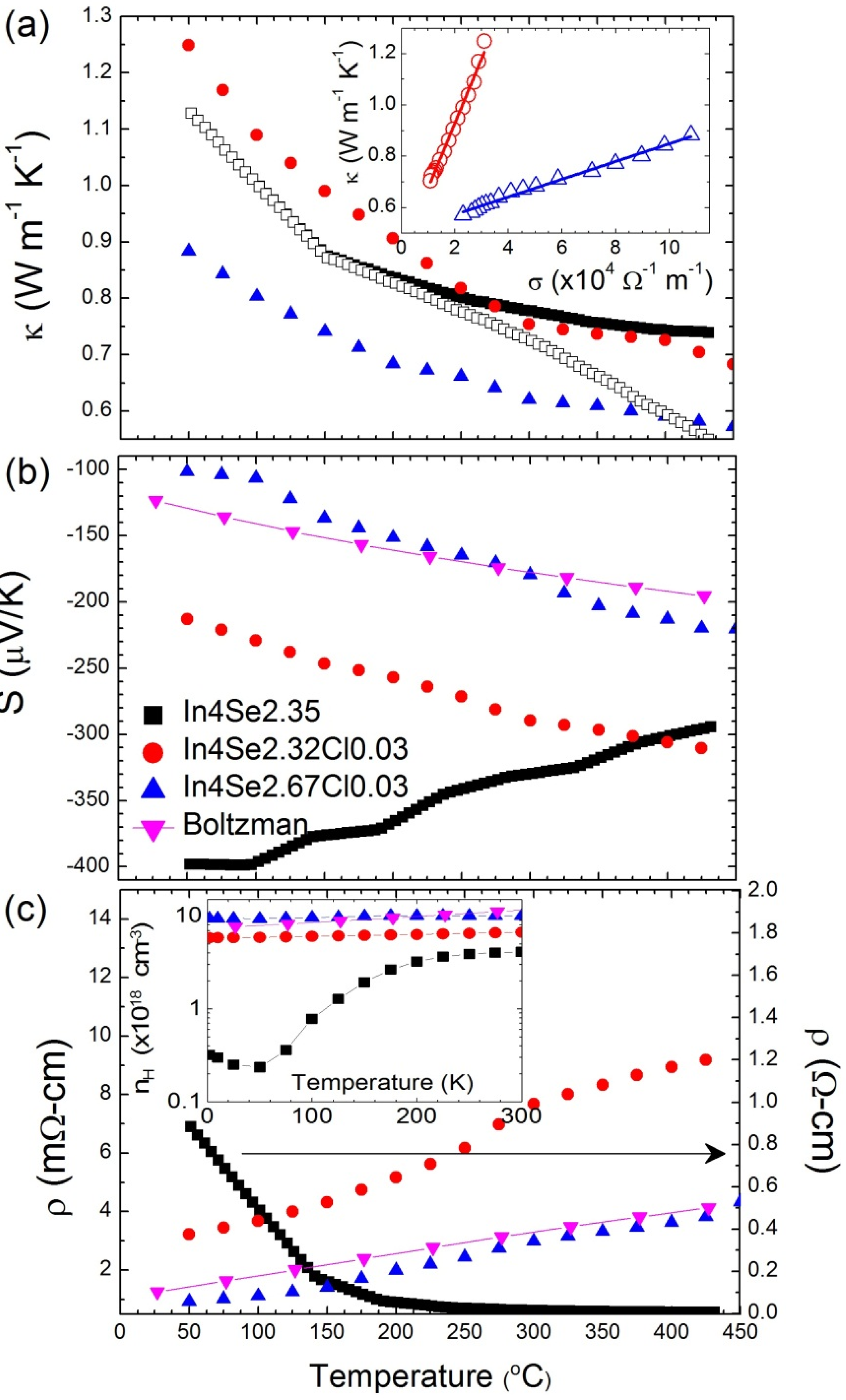
4Se
2.35 crystal for comparison. Because high thermoelectric performance was revealed along the
bc-plane of the crystal containing charge density wave lattice instability, the thermoelectric properties were measured along that plane. The inherent nature of van der Waals interactions along the
a-axis and Peierls distortion in the
bc-plane render the low thermal conductivity. The lattice thermal conductivity of In
4Se
2.35 crystal is obtained by subtracting the electronic thermal conductivity from the Wiedemann-Frantz (WF) law, as shown in the open rectangular symbol in
Figure 13a. However, the WF law is violated in a special case of bipolar transport [
8,
30]. An estimation of the lattice thermal conductivity can be made in a plot of
versus, which shows a linear relationship, as shown in the inset of
Figure 13a, because the thermal and electrical conductivities follow 1/
T temperature dependence in both cases. The extrapolation of the thermal conductivity to zero electrical conductivity gives the lattice thermal conductivity at a high temperature limit. A rough estimation of the high temperature lattice thermal conductivity of these compounds is presented in
Table 4. The estimated lattice thermal conductivities are not significantly changed by chlorine doping.
Figure 13.
Temperature-dependent thermoelectric properties of (
a) thermal conductivity, (
b) Seebeck coefficient, (
c) electrical resistivity, and Hall carrier concentration (inset of (
c)) for In
4Se
2.35 [
15], In
4Se
2.32Cl
0.03, and In
4Se
2.67Cl
0.03 bulk crystals [
29]. Reprodueced with permission from WILEY-VCH Verlag GmbH & Co., 2011 [
29].
The Seebeck coefficients decrease with chlorine doping in bulk crystal, as shown in
Figure 13b, because of the metallic behavior of electrical resistivity for chlorine-doped crystalline compounds, as shown in
Figure 13c. When chlorine is doped into In
4Se
3–δ crystal, the electrical resistivity decreases significantly (e.g., 0.92 mΩ·cm at 50 °C for In
4Se
2.67Cl
0.03) to two to three orders of magnitude lower than those of the undoped crystalline compound of In
4Se
2.35 (0.88 Ω·cm at 50 °C). The significant decrease of
is mainly a result of the increase in the Hall mobility as well as the increase in the carrier concentration, as shown in
Table 4. The improvement of the Hall mobility by chlorine doping can be attributed to the good alignment of the crystal along the
bc-plane parallel to the direction of the transport property measurements, as these compounds have highly anisotropic transport properties.
Table 4.
Estimated high-temperature lattice thermal conductivity
and room-temperature electrical resistivity
, carrier density
, Hall coefficient
, and Hall mobility
of the indicated crystalline samples.
Table 4.
Estimated high-temperature lattice thermal conductivity
and room-temperature electrical resistivity
, carrier density
, Hall coefficient
, and Hall mobility
of the indicated crystalline samples.
| Samples | (W·m−1·K−1) | (μΩ·m) | (×1018 cm−3) | (cm3/C) | (cm2·V−1·s−1) |
|---|
| In4Se2.35 | 0.54 | 8840 | 4.10 | 1.52 | 0.017 |
| In4Se2.32Cl0.03 | 0.43 | 32.24 | 6.70 | 0.93 | 2.889 |
| In4Se2.67Cl0.03 | 0.50 | 9.24 | 11.00 | 0.57 | 6.137 |
The temperature-dependent behavior of the Seebeck coefficient and electrical resistivity of In
4Se
2.67Cl
0.03 crystal can be reproduced by the Boltzmann transport calculation with a fixed chemical potential of μ = 0.36 eV, as shown in
Figure 13b,c (line and inverse triangle symbol). It was confirmed that the chemical potential of μ = 0.22 eV is comparable to the thermoelectric properties in In
4Se
2.35 crystal. The power factor with respect to the chemical potential from the Boltzmann transport calculation indicated that an increase of the chemical potential to μ = 0.8 eV can increase the power factor as a result of optimization of the carrier concentration. The increase in the chemical potential by chlorine doping (0.36 eV) has an effect on the electron doping, giving rise to an increase in the electronic carrier concentration (~10
19 cm
−3), as shown in the inset of
Figure 13c and in
Table 4.
More chlorine doping does not play a significant role in the electron doping because the solubility limit of the In
4Se
3−δ crystalline system is lower than 3 at.%, as confirmed by noting that the excess chlorine segregates to the surfaces of the crystal in depth profile measurements by secondary ion mass spectroscopy [
31]. The metallic behavior and relatively high Seebeck coefficients in the chlorine-doped In
4Se
3−xCl
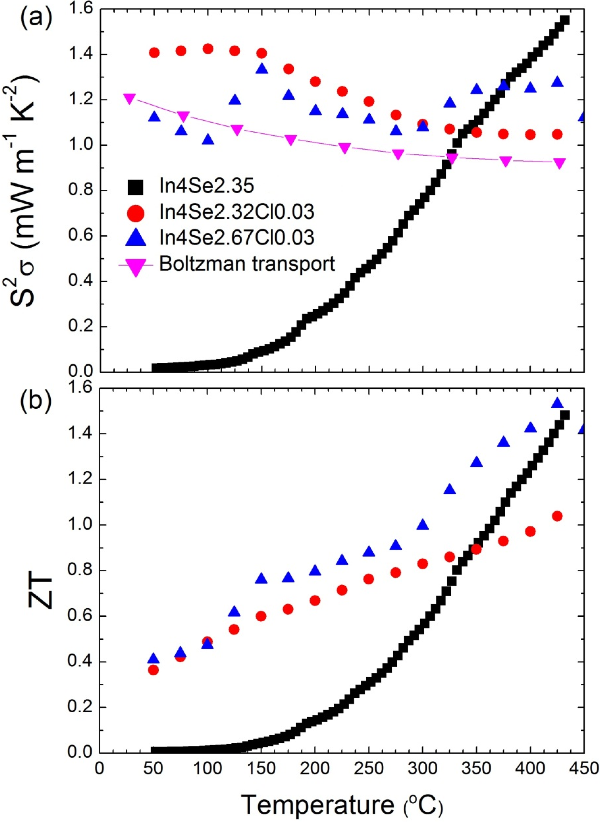
0.03 bulk single crystals lead to temperature-insensitive behavior of the power factor, as shown in
Figure 14a. Compared to the significant decrease of
as the temperature decreased in a previously reported case (black-closed square), the high power factors for a wide temperature range from 50 to 450 °C of chlorine-doped crystalline compounds are very important ingredients for practical applications owing to the possibility of stable power generation for such a wide temperature range. Because of a low thermal conductivity and high power factor, the
ZT of chlorine-doped crystals exhibits a high value in a broad temperature range, as presented in
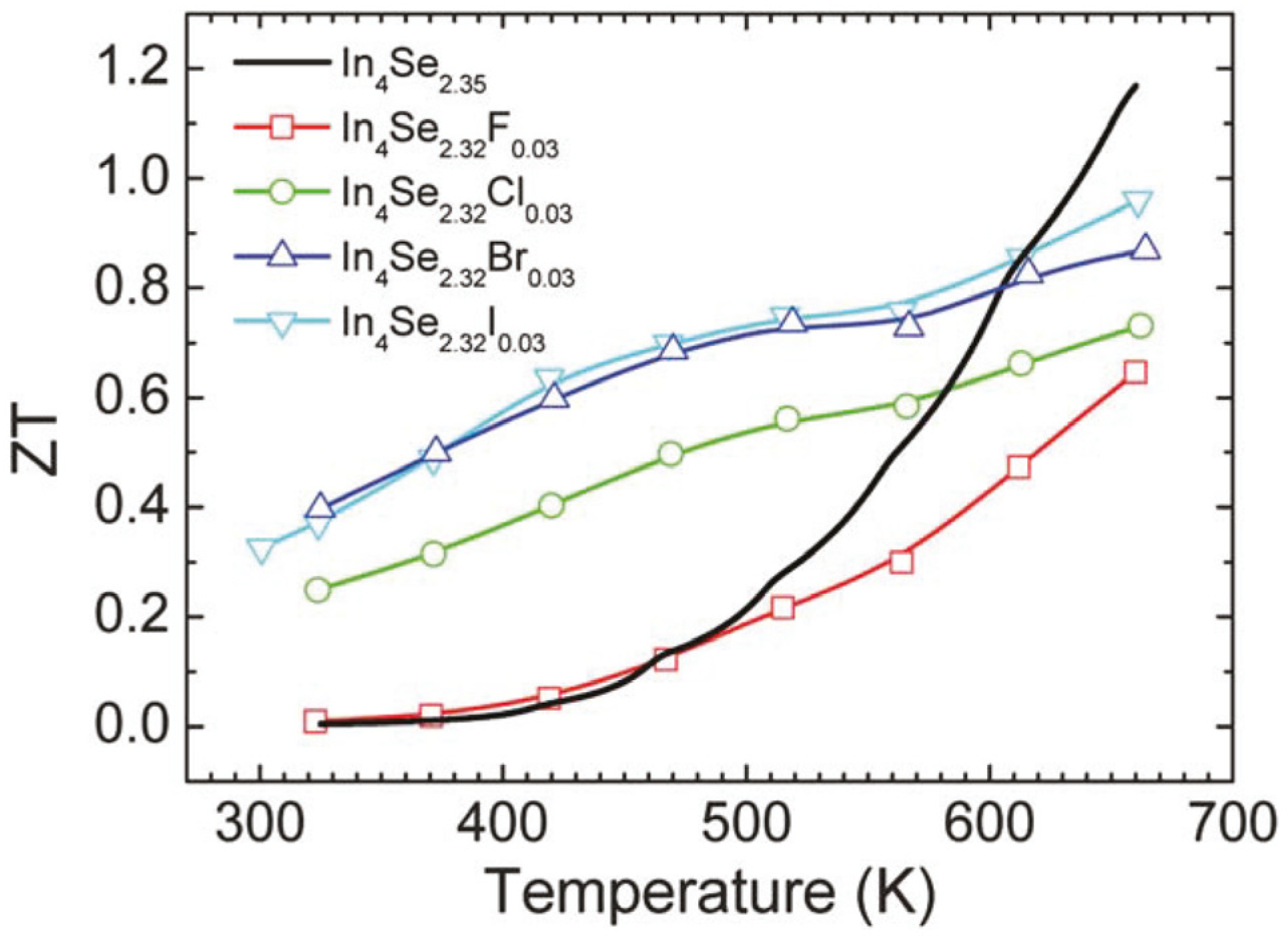
Figure 14b.
The
ZT maximum value reaches 1.53 at 425 °C, which increases
ZT further to the previously reported In
4Se
2.35 crystal (
ZT ~1.48) in
n-type materials [
15]. In addition, the room-temperature
ZT value increases significantly from 0.005 for In
4Se
2.35 to 0.4 for In
4Se
2.67Cl
0.03 crystals. When it is taken into account that the required
ZT for practical power generation is approximately 0.8, the operational temperature range (
) can be widened remarkably from 350~430 °C (
= 80 °C) for In
4Se
2.35 to 150~450 °C (
= 300 °C) for the In
4Se
2.67Cl
0.03 crystal.
Because chlorine doping is effective to enhance thermoelectric properties over a wide temperature range, we investigated the thermoelectric properties of other halogens including fluorine, bromine, and iodine substituted In
4Se
3−xH0.03 crystals in an effort to find a high
ZT material as well as to clarify the origin of a high
ZT in a chlorine substituted In
4Se
3−xCl
0.03 crystal [
32]. We show that both bromine and iodine-substituted In
4Se
3−xH0.03 crystals exhibit quite similar thermoelectric behaviors as the chlorine-substituted crystal. The fluorine-substituted crystal shows a quite different thermoelectric behavior compared to other halogens such as Cl-, Br-, and I-substituted crystals, but it is similar to the unsubstituted In
4Se
3−x crystal.
Figure 14.
Temperature-dependent (
a) power factor and (
b)
ZT value for In
4Se
2.35 [
15], In
4Se
2.32Cl
0.03, and In
4Se
2.67Cl
0.03 bulk crystals [
29]. Reproduced with permission from WILEY-VCH Verlag GmbH & Co., 2011 [
29].
Figure 14.
Temperature-dependent (
a) power factor and (
b)
ZT value for In
4Se
2.35 [
15], In
4Se
2.32Cl
0.03, and In
4Se
2.67Cl
0.03 bulk crystals [
29]. Reproduced with permission from WILEY-VCH Verlag GmbH & Co., 2011 [
29].
Figure 15a shows X-ray diffraction (XRD) patterns of the crystals of In
4Se
3−xH0.03 (
x = 0.68; H = F, Cl, Br, I). The X-ray diffraction patterns of the crystals were collected along their perpendicular planes to the crystal growth direction. The In
4Se
3−xH0.03 crystals exhibit nearly the same diffraction patterns indicating a similar preferred orientation of planes regardless of the kind of halogens such as F, Cl, Br, and I. The X-ray diffraction patterns on the cross-sectional planes being perpendicular to the growth direction of the crystals show that the growth direction of the crystals is mainly perpendicular to the
c-axis whereas minor random orientation peaks of {h31}, {h11}, and {h01} planes are observed.
Typical infrared absorption spectra for the powder samples of In
4Se
3−x (
x = 0.65) and In
4Se
3−xH0.03 (
x = 0.68;
H = F, Cl, Br, I) crystals are shown in
Figure 15b. All samples exhibit spectroscopically observable energy band gaps between 0.62 and 0.63 eV, which are consistent with a band gap between 0.5 and l.0 eV for In
4Se
3 with anisotropic band dispersions [
19]. This indicates that the halogen substitution on the In
4Se
3−x crystals does not influence on band gap widening despite of more electronegative character of halogen than selenium. Thus, the more ionic character in the In–H bond than the In–Se bond may result in the wider band gap in the In
4Se
3−xH0.03 crystal than the In
4Se
−x crystal. However, a nominal concentration of halogen-substitution in this work is just ~1.3 mol% on anionic sites, which may be too small to result in band gap widening.
Figure 15.
(
a) The X-Ray diffraction patterns perpendicular planes to the crystal growth direction and (
b) Infrared absorption spectra and of the crystals of In
4Se
3−xH0.03 (
x = 0.68;
H = F, Cl, Br, I) and In
4Se
2.35 [
32].
Figure 15.
(
a) The X-Ray diffraction patterns perpendicular planes to the crystal growth direction and (
b) Infrared absorption spectra and of the crystals of In
4Se
3−xH0.03 (
x = 0.68;
H = F, Cl, Br, I) and In
4Se
2.35 [
32].
The temperature dependent electrical conductivities of the crystals of In
4Se
3−x (
x = 0.65) and In
4Se
3−xH0.03 (
x = 0.68;
H = F, Cl, Br, I) are plotted in
Figure 16a. The thermoelectric properties were measured along the
bc-plane of the crystals because the electrical conduction is thought to be dominant along the plane [
8] and the high thermoelectric performance was revealed along the plane [
15]. Here, the electrical and thermal properties have been measured in the same direction.
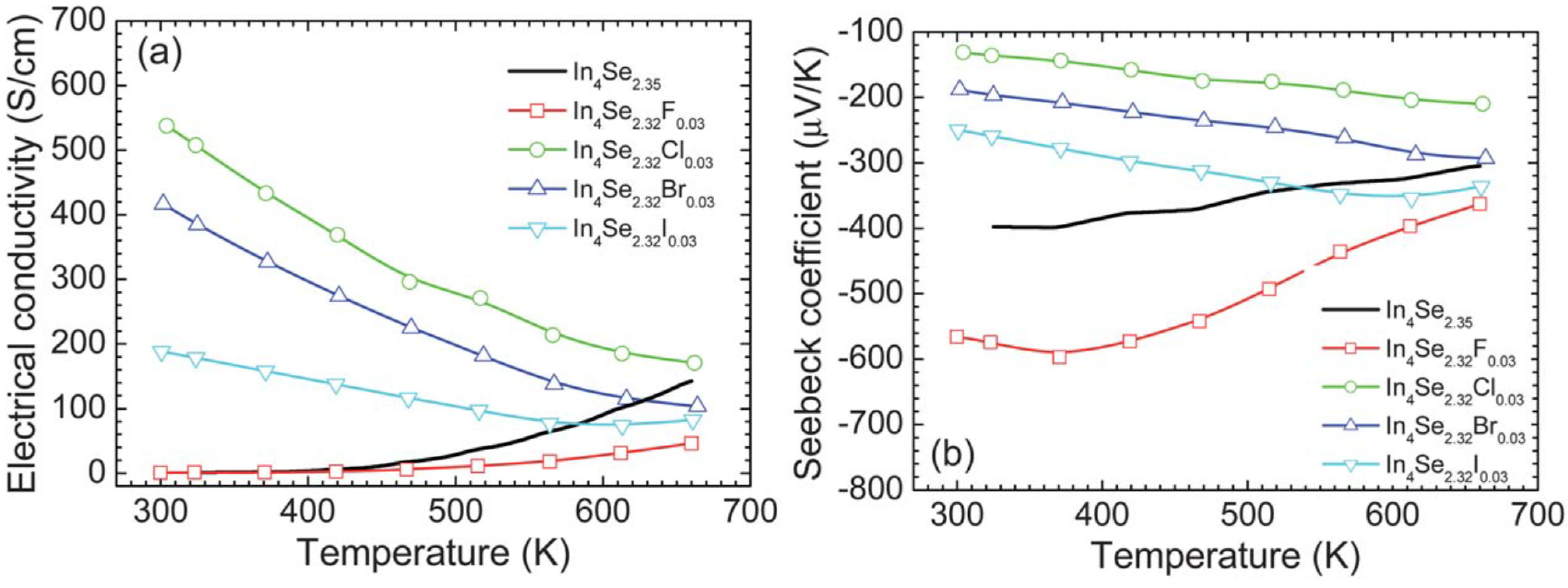
The room temperature electrical conductivities of the crystals of In4Se2.35, In4Se2.32F0.03, In4Se2.32Cl0.03, In4Se2.32Br0.03, and In4Se2.32I0.03 are ~1.1, ~0.9, ~537.6, ~416.7, and ~188.3 S/cm, respectively. The chlorine-, bromine-, and iodine-substituted In4Se3−xH0.03 crystals exhibit significantly higher room temperature electrical conductivities than the un-substituted and fluorine-substituted crystals. For instance, the crystal of In4Se2.32Cl0.03 shows ~500 times higher room temperature electrical conductivity than the crystal of In4Se2.35. The electrical conductivity σ is expressed as σ = neμ, where n is the carrier concentration, e the electrical charge, and μ the carrier mobility. The increase in σ should result from either (both) the increase in n or (and) the increase in μ. Carrier concentration of the crystals measured by Hall effect will be shown below in order to understand the origin of the increase in σ. The respective electrical conductivities at ~660 K of the crystals of In4Se2.35, In4Se2.32F0.03, In4Se2.32Cl0.03, In4Se2.32Br0.03, and In4Se2.32I0.03 are ~142.3, ~46.3, ~170.6, ~103.4, and ~82.6 S/cm. The chlorine-, bromine-, and iodine-substituted In4Se3−xH0.03 crystals show metallic (degenerate semiconducting) behaviors indicating that the electrical conductivity decreases with increasing temperature while the unsubstituted and fluorine substituted crystals display typical semiconducting behaviors.
Figure 16.
Temperature dependence of (
a) electrical conductivity and (
b) Seebeck coefficient of the crystals of In
4Se
3−xH0.03 (
x = 0.68; H = F, Cl, Br, I) and In
4Se
2.35 [
32].
Figure 16.
Temperature dependence of (
a) electrical conductivity and (
b) Seebeck coefficient of the crystals of In
4Se
3−xH0.03 (
x = 0.68; H = F, Cl, Br, I) and In
4Se
2.35 [
32].
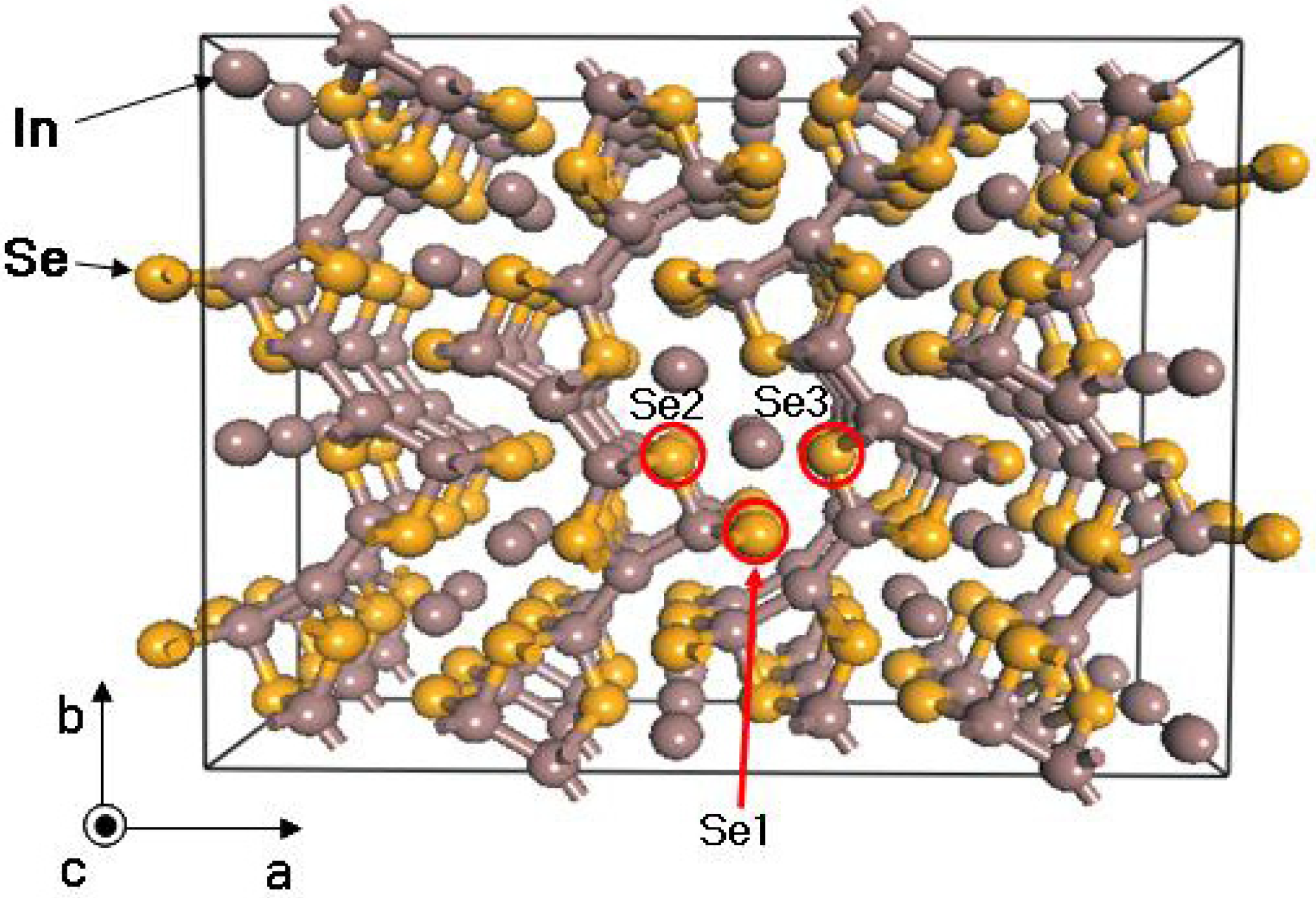
Table 5 shows both the electron concentrations and the Hall mobilities of the crystals of In
4Se
2.35, In
4Se
2.32F
0.03, In
4Se
2.32Cl
0.03, In
4Se
2.32Br
0.03, and In
4Se
2.32I
0.03. The room temperature electron concentrations show that the lighter and smaller halogen-substituted crystals display a slightly higher electron concentration, which is probably due to the atomic size difference between selenium and the halogens such as Cl, Br, and I. For instance, the empirically measured atomic radii of Se, F, Cl, Br, and I are 1.15, 0.5, 1, 1.15, and 1.40 Å, respectively [
33]. Compared to the atomic radius of selenium, the slightly smaller chlorine atom may be more easily occupied at the Se site in the lattice of the 4:3 indium selenide than the much smaller fluorine, the same size bromine, and the larger iodine atom. It has been reported that the crystal structure of In
4Se
3 consists of [(In
3)
5+(Se
3)
6−]
1− anionic layers (Se1, Se2, Se3 sites) and In
1+ cations with a weak van der Waals interaction along the
a-axis between the layers and strong covalent-ionic interaction in the
bc-planes within the layer [
17,
34,
35].
Table 5.
Formation energies in eV at each selenium site for the compositions of In
4Se
3−xH0.03 (
x = 0.06;
H = F, Cl, Br, I) and room temperature carrier concentrations and Hall mobilities of the crystals of In
4Se
3−xH0.03 (
x = 0.68;
H = F, Cl, Br, I) and In
4Se
2.35 [
32].
Table 5.
Formation energies in eV at each selenium site for the compositions of In4Se3−xH0.03 (x = 0.06; H = F, Cl, Br, I) and room temperature carrier concentrations and Hall mobilities of the crystals of In4Se3−xH0.03 (x = 0.68; H = F, Cl, Br, I) and In4Se2.35 [32].
| H | Se1 | Se2 | Se3 | nH (×1017 cm−3) | μ
H (cm2·V−1·s−1) |
|---|
| F | 1.46 | 1.54 | 1.31 | 0.45 | 124.8 |
| Cl | 1.27 | 1.14 | 1.12 | 41 | 819.5 |
| Br | 1.25 | 1.12 | 1.16 | 35 | 744.1 |
| I | 1.25 | 1.11 | 1.22 | 29 | 405.8 |
| In4Se2.35 | – | – | – | 41 | 1.7 |
The formation energies of the compositions of In
4Se
3−xH0.03 (
x = 0.06;
H = F, Cl, Br, I) at each Se sites (Se1, Se2, and Se3 site) were calculated within the density functional theory. The formation energies of the compositions of In
4Se
3−xH
0.03 (
x = 0.06; H = F, Cl, Br, I) at each Se site in
Table 5 show that the halogen-substitution at the Se3 site is energetically most favorable for H = F and Cl while the Se2 site is most preferable for H = Br and I. Based on the formation energy calculation results, the degree of energetic preference at a certain selenium site is approximately similar among different halogens. However, it is notable that the fluorine-substituted crystal does have a much lower electron concentration of the order of 10
16 cm
−3 than other halogen-substituted ones, which is even lower than that of the unsubstituted crystal of In
4Se
3−x (
x = 0.65). We may speculate that the fluorine element, unlike other halogen elements, may be preferentially occupied either at the Se vacancy sites (V
Se) or at the interstitial sites (I) in the lattice of In
4Se
3−x (
x = 0.65) rather than at the Se sites (Se) and thus the fluorine-substitution may decrease the electron concentration because of hole character of either the defect F
VSe1− (an atom of F located at the Se vacancy site) or the defect F
I1− (an atom of F located at the interstitial site) rather than electron character of the defect F
Se1+ (an atom of F located at the Se sublattice). We do another calculation of formation energies in order to clarify why the F-substituted sample has much lower electron concentration compared to the rest of samples.
Table 6 shows that the interstitial occupation of F is more energetically stable than the lattice substitution, whereas the opposite occurs for Cl, Br, and I. Our speculation regarding lower electron concentration in the fluorine-substituted sample is in good agreement with the calculations of formation energies. The chlorine-, bromine-, and iodine-substituted In
4Se
3−xH
0.03 crystals show electron concentrations comparable to the unsubstituted In
4Se
3−x crystal, while the fluorine-substituted crystal exhibits an electron concentration nearly two orders lower than the unsubstituted crystal. The Hall mobility μ
H is expressed as μ
H = σ
/ne = σ
RH, where
RH is the Hall coefficient of the crystals. Except for fluorine, it appears that the heavier halogen-substituted In
4Se
3−xH0.03 crystal shows a slightly lower Hall mobility because of stronger electron–phonon scattering for heavier halogen-substituted crystals, which is mainly due to the heavier atomic mass of the heavier halogen elements. It is quite notable that the halogen substituted In
4Se
3−xH0.03 crystals, even that with fluorine, exhibit significantly higher Hall mobilities than the unsubstituted crystal. For instance, the room temperature Hall mobility of the crystal of In
4Se
2.32Cl
0.03 is ~500 times higher than the unsubstituted crystal of In
4Se
2.35. Thus, the substantial increase in electrical conductivity of the halogen-substituted In
4Se
3−xH0.03 crystals should result from a remarkable increase in Hall mobility.
Table 6.
Formation energies in eV for the compositions of In
4Se
2.94H
0.06 (substitution), In
4Se
2.88H
0.06 (substitution + vacancy), and In
4Se
3H
0.06 (interstitial) [
32].
Table 6.
Formation energies in eV for the compositions of In4Se2.94H0.06 (substitution), In4Se2.88H0.06 (substitution + vacancy), and In4Se3H0.06 (interstitial) [32].
| Halogen | Substitution | Substition + Vacancy | Interstitial |
|---|
| F | 1.31 | 1.04 | 0.60 |
| Cl | 1.12 | 1.02 | 1.28 |
| Br | 1.12 | 0.98 | 1.37 |
| I | 1.11 | 0.97 | 1.42 |
Usually, one observes degradation of mobility upon substitution, which is mainly due to enhanced carrier scattering. However, the experimental observation of enhanced carrier mobility upon halogen-substitution is interesting and thus it is useful to further elucidate the reason of the enhanced mobility, at least some possible explanations. We may speculate that either the electron scattering may be weakened through the halogen-substitution for some reason, or that the charge scattering mechanism of the halogen-substituted In
4Se
3−xH0.03 crystals may be quite different compared to that of the unsubstituted In
4Se
3−x crystal, thus resulting in a significant enhancement of the Hall mobility of the halogen-substituted crystals. A detailed analysis of the charge scattering mechanism would be desirable and thus we utilized a single parabolic band (SPB) model [
36] to obtain room temperature carrier mobilities of the halogen-substituted In
4Se
3−xH0.03 crystalline samples. The SPB model is derived from solutions to the Boltzmann transport equation within the relaxation time approximation. The reduced chemical potential across measured temperature range is firstly estimated in the SPB model from temperature dependent Seebeck coefficient. The effective mass is secondly estimated from the experimental carrier concentration and reduced chemical potential. The carrier mobility is finally estimated from the effective mass and a constant relaxation time of 2.2 × 10
−14 s which was used in reference [
11] (see Equation (5) in reference [
32]).
Table 7 shows calculated effective masses and carrier mobilities of the samples at the assumption of acoustic phonon scattering within the framework of Boltzmann transport equation. For example, the carrier mobility of 130 cm
2·V
−1·s
−1 was estimated in the Cl-substituted crystalline sample with the assumption of acoustic phonon scattering while that of 819.5 cm
2·V
−1·s
−1 was experimentally obtained. There is a large discrepancy between the experimental carrier mobility and the estimated carrier mobility. Therefore, we believe that either a combination of charge scatterings including acoustic phonon scattering, ionized impurity scattering, and neutral impurity scattering can govern the charge scattering mechanism of the halogen-substituted samples or the SPB model can fail because of multiple bands contributing in the 4:3 indium selenide like heavy and light hole band in PbTe or nonparabolicity present in almost all systems.
Table 7.
Room temperature properties of In
4Se
2.35 and In
4Se
3−xH
0.03 (
x = 0.68; H = F, Cl, Br, I) crystalline samples, where the calculated
mcal* and
mcal are obtained assuming acoustic phonon scattering within the framework of Boltzmann transport equation [
32].
Table 7.
Room temperature properties of In4Se2.35 and In4Se3−xH0.03 (x = 0.68; H = F, Cl, Br, I) crystalline samples, where the calculated mcal* and mcal are obtained assuming acoustic phonon scattering within the framework of Boltzmann transport equation [32].
| Composition | μ
H (cm2·V−1·s−1) | μ
cal (cm2·V−1·s−1) | mcal* (me) |
|---|
| In4Se2.35 | 1.7 | 19 | 1.75 |
| In4Se2.32F0.03 | 124.8 | 98 | 0.35 |
| In4Se2.32Cl0.03 | 819.5 | 130 | 0.19 |
| In4Se2.32Br0.03 | 744.1 | 97 | 0.30 |
| In4Se2.32I0.03 | 405.8 | 70 | 0.45 |
Figure 16b shows the Seebeck coefficient as a function of temperature for the crystals of In
4Se
3−x (
x = 0.65) and In
4Se
3−xH
0.03 (
x = 0.68; H = F, Cl, Br, I). The quasi-onedimensional In–Se chain in the CDW plane for the 4:3 indium selenide is a main factor contributing to the thermoelectric performance, which is because of the enhancement on the Seebeck coefficient due to the In–Se chain (quantum confinement) as well as the reduction on the lattice thermal conductivity due to the Peierls distortion in the CDW plane.
The absolute values of Seebeck coefficient of the chlorine-, bromine-, and iodine-substituted In
4Se
3−xH
0.03 crystals increase with increasing temperature, which is consistent with their electrical conductivity behaviors. It has been reported that the chlorine doping on In
4Se
3−x only increased its chemical potential, giving rise to an increase in the electron concentration and thus the temperature dependent Seebeck coefficient of the chlorine doped crystal was able to be reproduced by the Boltzmann transport calculation with a fixed chemical potential [
29]. This implies that the halogen-substitution on In
4Se
3−x should not weaken the role of the In–Se chain on Seebeck coefficient compared to the halogen-free In
4Se
3−x crystals. The corresponding temperature dependent power factors of the unsubstituted and halogen substituted crystals are plotted in
Figure 17a.
Figure 17.
Temperature dependence of (
a) power factor and (
b) thermal conductivity of the crystals of In
4Se
3−xH
0.03 (
x = 0.68; H = F, Cl, Br, I) and In
4Se
2.35 [
32].
Figure 17.
Temperature dependence of (
a) power factor and (
b) thermal conductivity of the crystals of In
4Se
3−xH
0.03 (
x = 0.68; H = F, Cl, Br, I) and In
4Se
2.35 [
32].
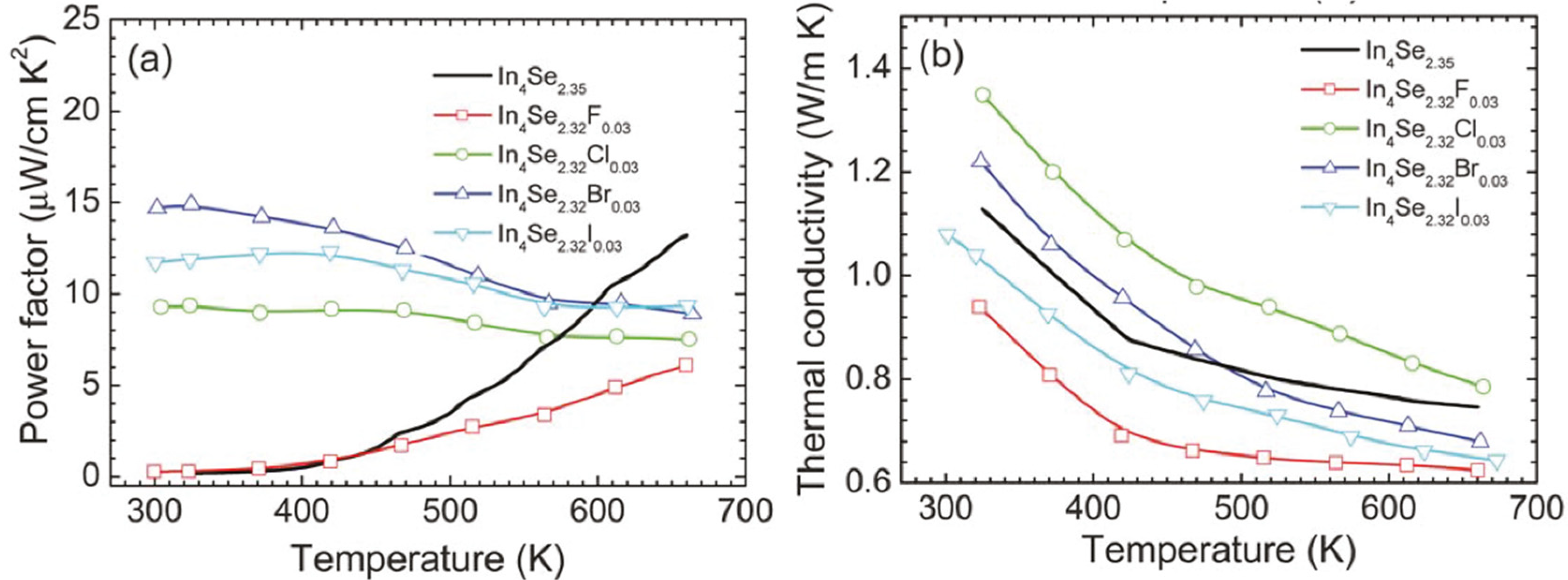
It is quite notable that, except for fluorine, the room temperature power factors of the halogen-substituted crystals are significantly higher than that of the unsubstituted crystal, which is mainly due to the significant increase in the electrical conductivity. For instance, the bromine-substituted crystal shows a room temperature power factor which is approximately 80 times higher than the unsubstituted crystal. This indicates that the power factors of the chlorine-, bromine-, and iodine-substituted crystals slightly decrease with a rise in temperature while those of the unsubstituted and fluorine-substituted crystals rapidly increases with increasing temperature.
Figure 17b shows the temperature dependent total thermal conductivities of the crystals of In
4Se
3−x (
x = 0.65) and In
4Se
3−xH0.03 (
x = 0.68;
H = F, Cl, Br, I). The total thermal conductivities of all the crystals decrease with increasing temperature. The room temperature total thermal conductivities of the crystals ranges from 1.1 ~ 1.3 W·m
−1·K
−1, respectively. Thus, the room temperature lattice thermal conductivities are expected to be 0.9~1.1 W·m
−1·K
−1 when the Lorenz number is assumed to be 2.45 × 10
−8 V
2·K
−2 for degenerate semiconductor. These are substantially low at room temperature, which is comparable to nanostructured LAST (Pb–Ag–Sb–Te) and Bi–Sb–Te samples [
25,
29]. Based on the expected room temperature lattice thermal conductivity data, the halogen-substitution may not have a negative influence on the effect of the Peierls distortion on the reduction in the lattice thermal conductivity.
Figure 18 shows the dimensionless thermoelectric figure of merit
ZT as a function of temperature for the unsubstituted and halogen-substituted crystals. The
ZT increases with increasing temperature. It is quite notable that the room temperature
ZT values of the Cl-, Br- and I-substituted crystals are substantially higher than that of the unsubstituted crystal. For instance, the room temperature
ZT of the crystal of In
4Se
2.32Cl
0.03 is about 40 times higher than that of the crystal of In
4Se
2.35. The respective
ZT values at 660 K for the crystals of In
4Se
2.35, In
4Se
2.32F
0.03, In
4Se
2.32Cl
0.03, In
4Se
2.32Br
0.03, and In
4Se
2.32I
0.03 are 1.2, 0.6, 0.7, 0.9, and 1.0. Note that the crystal of In
4Se
2.67Cl [
29] has been reported to exhibit a higher
ZT than the crystal of In
4Se
2.32Cl
0.03, and thus we grew the crystals of In
4Se
2.67H
0.03 (H = F, Br, I) and measured their thermoelectric properties. However, the
ZT values of the crystals of In
4Se
3−xH
0.03 (H = F, Br, I) were unfortunately nearly as same as those of the crystals of In
4Se
2.32H
0.03 (H = F, Br, I). Therefore, in this work we only focused on the improvement of thermoelectric performance in the crystals of In
4Se
2.32H
0.03 (H = F, Cl, Br, I) compared to the crystal of In
4Se
2.35.
Figure 18.
Temperature dependence of the thermoelectric figure of merit of the crystals of In
4Se
3−xH
0.03 (
x = 0.68; H = F, Cl, Br, I) and In
4Se
2.35 [
32].
Figure 18.
Temperature dependence of the thermoelectric figure of merit of the crystals of In
4Se
3−xH
0.03 (
x = 0.68; H = F, Cl, Br, I) and In
4Se
2.35 [
32].
2.3.3. Multiple Elements Doping and Selenium Deficiency in Polycrystalline In4Pb0.01Sn0.03Se3−x Compounds
Recently, the high
ZT = 1.4 at 733 K for Pb-/Sn-codoped In
4Pb
xSn
ySe
3 polycrystalline compounds was reported [
37]. The Boltzmann transport calculation of In
4Se
3−δ shows that the high power factor
S2σ can be expected for increasing chemical potential, in other words electron doping [
15,
29]. In our previous study, the cationic elements substitution was not effective due to the decrease of carrier mobility [
27]. Lin
et al. noticed that the Pb and Sn substitute at different In-sites (In4 and In2 sites respectively) when they re-examine the formation energy calculation of In
4Se
3 [
27]. The crystal structure of In
4Se
3 consists of In
1+ cations and [(In
3)
5+(Se
3)
6−]
1− anionic staking layers along the
a-axis [
35,
38,
39].
Despite non-systematic dependence on the Pb and Sn concentrations, it is believed that the co-doping is very effective for increasing
ZT value of In
4Se
3 phase [
37]. In the In
4Se
3 system, the Se-deficiency is very important for high thermoelectric performance. The non-stoichiometric Se-deficiency has an effect of hole localization with dispersive electron conduction resulting in the quasi-one-dimensional electronic transport [
21]. From the formation energy calculation, the Se deficiency is in the [(In
3)
5+(Se
3)
6−]
1− anionic layer of the In
4Se
3 structure. The vacant site of a dangling bonded Se (Se3 site) is more stable than other Se sites. The theoretical calculation proved that the Se vacancy strongly suppresses phonon propagation along the plane of charge density wave [
39]. In addition, the Se deficiency of the In
4Se
3−x can decrease the electrical resistivity by increasing carrier concentration [
21,
40,
41] as well as the Hall mobility (μ
H) [
21,
42]. Therefore, we studied the Se deficiency effect on the Pb-/Sn-codoped In
4Pb
0.01Sn
0.03Se
3−x polycrystalline compounds.
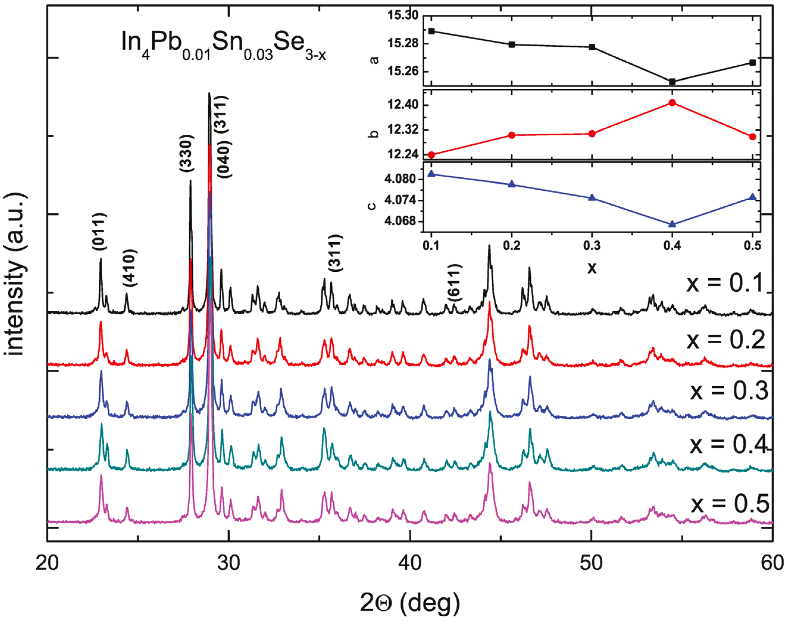
Figure 19 shows the powder XRD pattern of the annealed In
4Pb
0.01Sn
0.03Se
3−x (
x = 0.1, 0.2, 0.3, 0.4, and 0.5) polycrystalline compounds [
43]. The patterns represent a single phase of In
4Se
3 with no distinguishable impurity phases. The inset of
Figure 19 depicts the lattice parameters of In
4Pb
0.01Sn
0.03Se
3−x polycrystalline compounds with different Se-deficiency. The lattice parameters of
a- and
c-axis are systemically decreased and
b-axis is increased with increasing Se deficiency from
x = 0.1 to 0.4 indicating systematic control of Se deficiency. For
x = 0.5 compound, the lattice parameters are abruptly changed, indicating the solubility limit of Se-deficiency. From the crystal structure of In
4Se
3, the Se vacancy is energetically favorable at the dangling bonded Se3-site [
19,
37]. If the vacancy in the Se3-site is employed, the charge re-distribution can relax the cluster. Therefore we anticipate that the lattice is elongated along the
b-axis while the lattices along the
a- and
c-axis are compressed due to the cluster distortion.
Figure 19.
The powder X-ray diffraction patterns of In
4Pb
0.01Sn
0.03Se
3−x (
x = 0.1, 0.2, 0.3, 0.4, and 0.5) polycrystalline compounds. The inset shows the lattice parameters of the compounds. Reproduced with permission from Elsevier B.V., 2014 [
43].
Figure 19.
The powder X-ray diffraction patterns of In
4Pb
0.01Sn
0.03Se
3−x (
x = 0.1, 0.2, 0.3, 0.4, and 0.5) polycrystalline compounds. The inset shows the lattice parameters of the compounds. Reproduced with permission from Elsevier B.V., 2014 [
43].
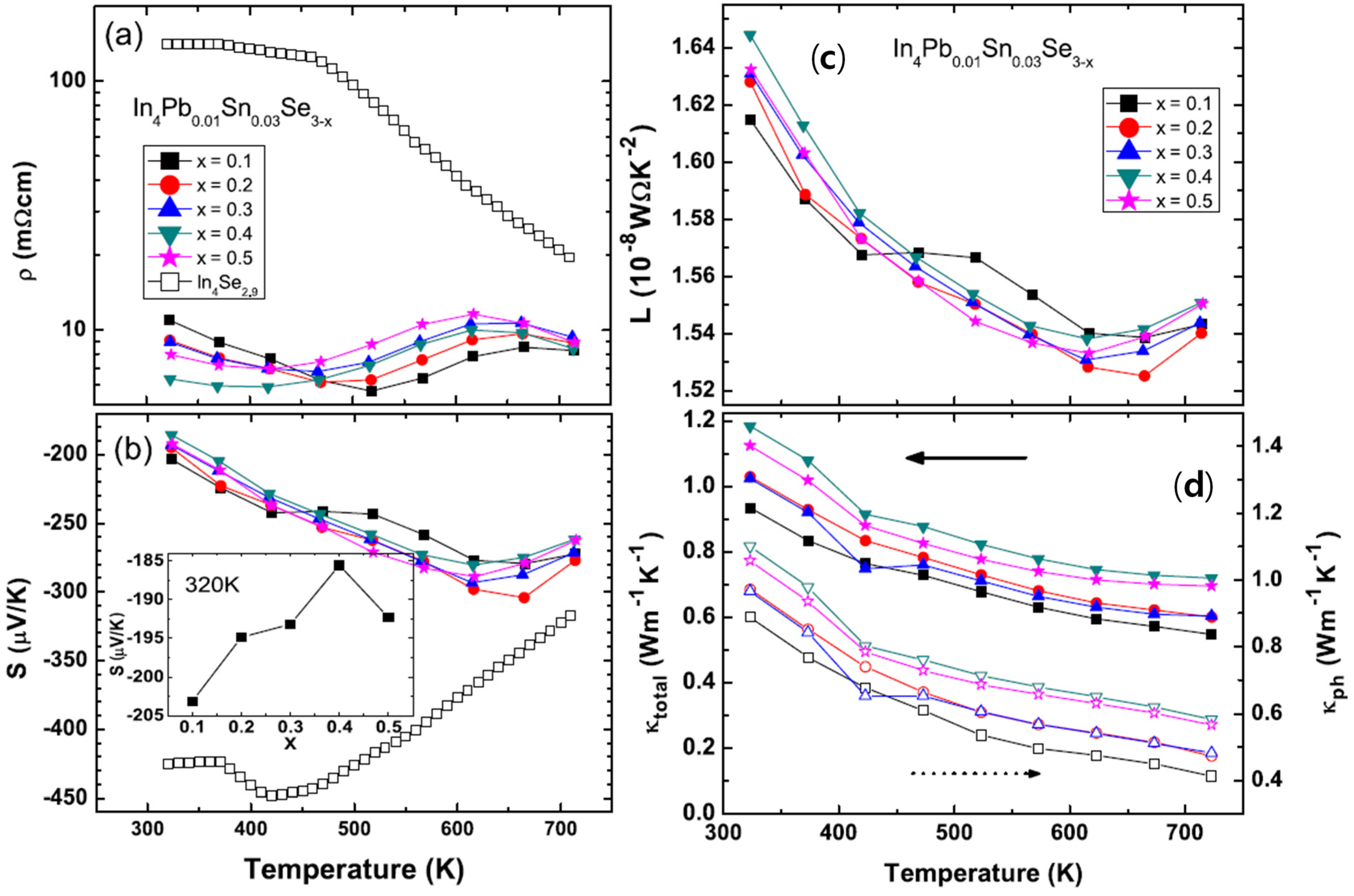
The temperature dependent electrical resistivities ρ
(T) of polycrystalline compounds In
4Pb
0.01Sn
0.03Se
3−x (
x = 0.1, 0.2, 0.3, 0.4, and 0.5) [
43] and In
4Se
2.9 (open square for comparison [
21]) are presented in
Figure 20a. The ρ
(T) of Pb-/Sn-codoped polycrystalline compound In
4Pb
0.01Sn
0.03Se
2.9 is significantly decreased than the one of In
4Se
2.9. The ρ
(T) s near room temperature of Pb-/Sn-codoped and Se-deficient polycrystalline compounds are decreased with increasing Se-deficiency except for x = 0.5 case. The decrease of electrical resistivity is similar to those of In
4Se
3−x polycrystalline compounds [
21,
40,
41,
44]. From the effective carrier concentration
nH and Hall mobility μ
H, calculated by Hall resistivity ρ
xy measurement (
Table 8), the carrier concentrations are increased with increasing Se-deficiency while electrical resistivity and Hall mobility of the compounds are decreased up to
x = 0.4. The Pb-/Sn-codoping significantly increase the carrier density from 2.09 × 10
17 cm
−3 for polycrystalline compounds of In
4Se
2.9 [
21] to 2.67 × 10
18 cm
−3 for In
4Pb
0.01Sn
0.03Se
2.9.
Figure 20.
Temperature-dependent electrical resistivity ρ
(T) (
a), Seebeck coefficient
S(T) (
b), Temperature-dependent Lorenz number
L (
c), total thermal conductivity κ
tot (closed symbols, left axis) and lattice thermal conductivity κ
ph (open symbols, right axis) (
d) of In
4Pb
0.01Sn
0.03Se
3−x (
x = 0.1, 0.2, 0.3, 0.4, and 0.5) polycrystalline compounds. Reproduced with permission from Elsevier B.V., 2014 [
43].
Table 8.
The Hall carrier density
, electrical resistivity
, Hall mobility
, Seebeck coefficient
S and effective mass of electron
m* of In
4Pb
0.01Sn
0.03Se
3−x (
x = 0.1, 0.2, 0.3, 0.4, and 0.5) polycrystalline compounds. Reproduced with permission from Elsevier B.V., 2014 [
43].
Table 8.
The Hall carrier density , electrical resistivity
, Hall mobility , Seebeck coefficient S and effective mass of electron m* of In4Pb0.01Sn0.03Se3−x (x = 0.1, 0.2, 0.3, 0.4, and 0.5) polycrystalline compounds. Reproduced with permission from Elsevier B.V., 2014 [43].
| x | (1018 cm−3) | (mΩ·cm) | (cm2·V−1·S−1) | (μV/K) | () |
|---|
| 0.1 | 2.67 | 10.944 | 213.60 | −203.14 | 0.182 |
| 0.2 | 4.16 | 9.056 | 165.67 | −194.87 | 0.235 |
| 0.3 | 4.99 | 8.925 | 140.14 | −193.20 | 0.263 |
| 0.4 | 6.26 | 6.332 | 157.46 | −185.56 | 0.294 |
| 0.5 | 4.37 | 7.928 | 180.15 | −192.32 | 0.240 |
There are broad humps of electrical resistivity near 600~650 K. The peak positions of ρ
(T) are decreased with increasing Se-deficiency from 665 K (
x = 0.1) to 615 K (
x = 0.5). From the thermal measurements of thermogravimetric and differential thermal analysis (TG/DTA), we do not find any phase transformation at those temperatures. The broad increase of resistivity is observed at a charge density wave instability [
7,
45]. One possibility of the broad humps is caused by the charge density wave phase transitions [
15]. However, it should be investigated as a further research to clarify the origin of abnormal increase of resistivity.
The temperature dependent Seebeck coefficients
S(T) of In
4Pb
0.01Sn
0.03Se
3−x (
x = 0.1, 0.2, 0.3, 0.4, and 0.5) and In
4Se
2.9 polycrystalline compounds are shown in
Figure 20b. Because the ρ
(T)s are significantly decreased, the
S(T) values are decreased for the Pb-/Sn-codoped polycrystalline compounds comparing with In
4Se
2.9. The maximum values of absolute Seebeck coefficients are appeared near the temperatures close to the temperature of broad shoulder in the electrical resistivity. The thermal band gap (
Eg) can be roughly estimated by the maximum Seebeck coefficient (
Smax) and the temperature of the
Smax, as following relation:
Eg =
2eSmaxTmax, where
e is the electron charge [
46]. The energy gaps are obtained ranging from 0.34 to 0.40 eV which are smaller than the one of In
4Se
3 (0.42 eV) [
42]. The smaller thermal band gap of the compounds than the one of stoichiometric In
4Se
3 may come from the change of band structure by Pb-/Se-codoping and Se-deficiency. As shown in the inset of
Figure 20a,b, the absolute Seebeck coefficients at room temperature follow the trade-off relationship with electrical resistivity.
Figure 20c shows the temperature dependent Lorenz number
L [
43]. The Lorenz numbers are very low compared with
L0 = 2.45 × 10
−8 W·Ω·K
−2. The low Lorenz numbers of the compounds may be affected by the change of Fermi energy [
47]. From the obtained Lorenz number, we can calculate the lattice thermal conductivity κ
ph. The total thermal conductivity κ (closed symbols, left axis) and lattice thermal conductivity κ
ph (open symbols, right axis) are presented in
Figure 20d. The κ and κ
ph are increased with increasing Se-deficiency. It is consistent with the result of In
4Se
3−x for high Se-deficiency (
x > 0.05) [
21]. The total thermal conductivity of In
4Se
3−x (
x > 0.05) is increased with increasing Se-deficient [
21].
Basically, the low thermal conductivity of In
4Se
3 based compounds comes from the Peierls distortion due to quasi-onedimensional lattice and charge density wave instabilities [
15]. Recent theoretical calculation of thermal conductivity by molecular dynamic simulation showed the Se-vacancy induces discontinuous charge density which causes the decrease of phonon transport [
39]. In terms of this interpretation, the Pb- and Sn-codoped polycrystalline compounds might have a different charge density distribution. The employment of Se-vacancy can interact with Pb- and Sn-cation substitutions and has a role of the weakness of the decrease of phonon propagation, resulting in the increase of thermal conductivity by increasing Se-deficiency. The detailed phonon dispersion relation should be investigated in order to understand those phenomena.
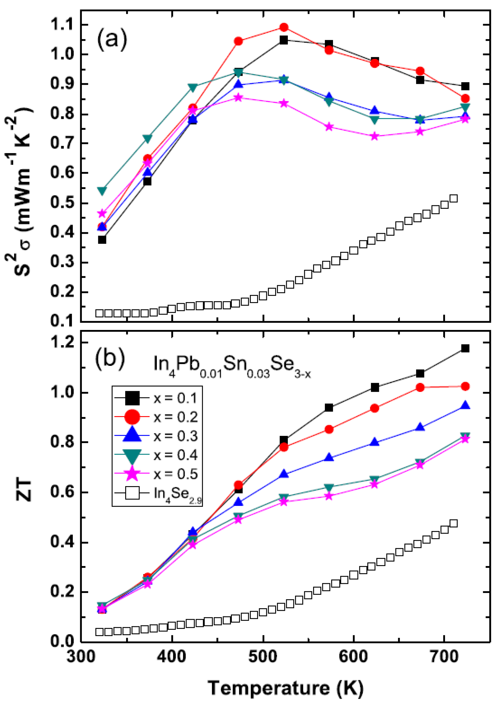
The temperature dependent power factors
S2σ of polycrystalline In
4Pb
0.01Sn
0.03Se
3−x (
x < 0.5) and In
4Se
2.9 are presented in
Figure 21a. The power factors of the Se-deficient and Pb-/Sn-codoped polycrystalline compounds (0.37–0.55 mW·m
−1·K
−2) have higher power factor than the ones of In
4Pb
0.01Sn
ySe
3 (0.1~0.19 mW·m
−1·K
−2) [
29] near room temperature. Comparing with the In
4Se
2.9, the Pb-/Sn-codoped and Se-deficient compounds have significantly enhanced values of the power factor. The high power factor over a wide temperature range (450 K ≤
T ≤ 725 K) is very important ingredient for practical thermoelectric applications.
The thermoelectric figure-of-merit
ZT of In
4Pb
0.01Sn
0.03Se
3−x (
x < 0.5) are increased with increasing temperature as shown in
Figure 21b. The maximum
ZT value reaches up to 1.2 at 723 K for polycrystalline In
4Pb
0.01Sn
0.03Se
3−x (
x = 0.1). Even though the
ZT value of the
x = 0.1 compound is lower than the one of In
4Pb
0.01Sn
0.03Se
3 (1.4 at 733 K) [
37], if we define the operational temperature
Top range as the temperature range for
ZT > 1.0, the operational temperature range of
x = 0.1 Se-deficient and Pb-/Sn-codoped polycrystalline compound (
Top > 600 K) is a little bit increased rather than those of In
4Pb
0.01Sn
0.03Se
3 compound (
Top > 620 K). In addition, the
ZT values of In
4Se
3−x significantly increased in the Pb-/Sn-codoped and Se-deficient polycrystalline compounds.
Figure 21.
Temperature-dependent power factor
S2σ (
a), and dimensionless figure-of-merit
ZT (
b) of In
4Pb
0.01Sn
0.03Se
3−x (
x = 0.1, 0.2, 0.3, 0.4, and 0.5) polycrystalline compounds. Reproduced with permission from Elsevier B.V., 2014 [
43].
Figure 21.
Temperature-dependent power factor
S2σ (
a), and dimensionless figure-of-merit
ZT (
b) of In
4Pb
0.01Sn
0.03Se
3−x (
x = 0.1, 0.2, 0.3, 0.4, and 0.5) polycrystalline compounds. Reproduced with permission from Elsevier B.V., 2014 [
43].
2.3.4. Multiple Elements Doping with Chlorine Doping and Selenium Deficiency in In4Pb0.01Sn0.03Se2.9Clx Polycrystalline Compounds
The halogen elements doping in the In
4Se
3 crystalline compounds In
4Se
3−xH
y (H = F, Cl, Br, and I) is a good candidate to enhance chemical potential [
32]. The Hall mobilities of the single crystalline In
4Se
3−xH
0.03 are significantly increased by halogen doping. It was found that the Cl-doping is the most effective for increase of Hall mobility. The polycrystalline In
4Pb
0.01Sn
0.03Se
2.9 compounds showed maximum
ZT value of 1.2 at 723 K [
43]. However, the power factor of the In
4Pb
0.01Sn
0.03Se
2.9 polycrystalline compound can increase furthermore because it is still far from the optimized chemical potential 0.8 eV from the Boltzmann transport calculation [
15,
29]. The chemical potential of the In
4Se
3 phase can be more increased by electron doping. The Cl-doping is believed to be a good candidate to increase thermoelectric performance in the multiple elements-doped In
4Pb
0.01Sn
0.03Se
2.9Cl
x compounds.
Figure 22 shows Rietveld refinement analysis on powder X-ray diffraction (XRD) patterns of the prepared samples (
x = 0.02 and
x = 0.04) based on the orthorthombic
Pnnm space group, respectively. The XRD patterns show a single phase of In
4Se
3 with no noticeable impurity peaks except
x = 0.06. Because of impurity phase of InSe (Hexagonal, No. 194), we cannot analyze the XRD pattern by Rietveld refinement for the
x = 0.06 compound. This indicates that
x = 0.06 is the solubility limit of chlorine which induces the phase separation from In
4Se
3 to InSe phase. The lattice parameter is calculated as shown in
Table 9. In the previous investigation of Se-deficient Pb/Sn co-doped polycrystalline compounds In
4Pb
0.01Sn
0.03Se
3−x (
x = 0.1, 0.2, 0.3, 0.4, and 0.5), the lattice parameters are systemically changed [
43]. However, the lattice parameters of Cl-doped samples In
4Pb
0.01Sn
0.03Se
2.9Cl
x do not show the systematic changes but show a decrease of lattice volume (inset of
Figure 22) with increasing chlorine concentration up to
x = 0.04 compound. Because the compound of
x = 0.06 has InSe impurity phase, the lattice volume of the compound does not show systematic change.
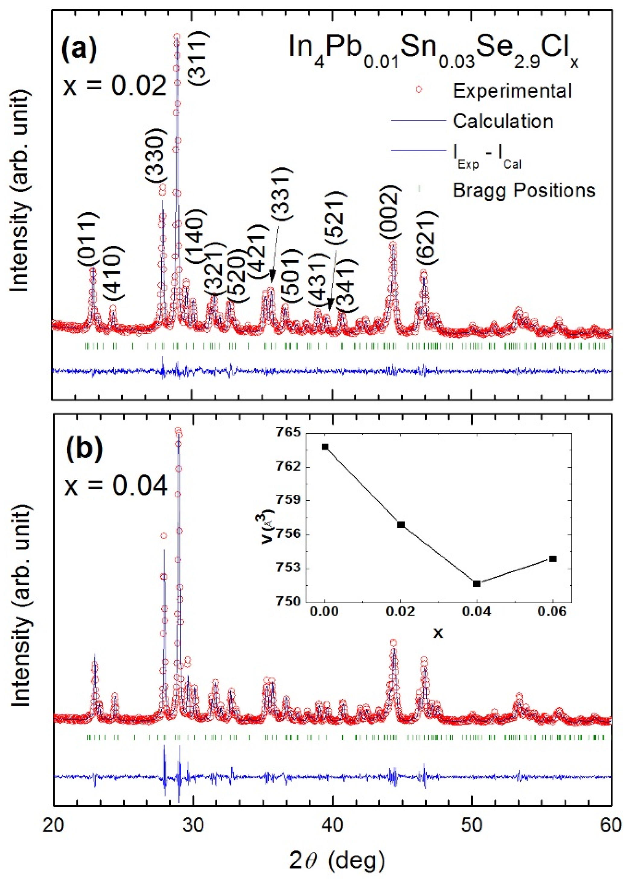
Figure 22.
Powder X-ray diffraction profiles of In
4Pb
0.01Sn
0.03Se
2.9Cl
x polycrystalline compounds (
a)
x = 0.02 and (
b)
x = 0.04. Reliability factors (R-factor) obtained from the fitting are as follows.
x = 0.02:
Rp = 6.75,
Rwp = 8.78,
Rexp = 7.30;
x = 0.04:
Rp = 9.10,
Rwp = 11.3,
Rexp = 7.34. Inset of (
b) shows the lattice volume with respect to Cl concentration of the compounds [
48].
Table 9.
The lattice parameters of In
4Pb
0.01Sn
0.03Se
2.9Cl
x (
x = 0.0, 0.02, 0.04, and 0.06) polycrystalline compounds [
48].
Table 9.
The lattice parameters of In4Pb0.01Sn0.03Se2.9Clx (x = 0.0, 0.02, 0.04, and 0.06) polycrystalline compounds [48].
| x | a (Å) | b (Å) | c (Å) | V (Å3) |
|---|
| 0.00 [43] | 15.29 | 12.24 | 4.08 | 764 |
| 0.02 | 15.19 | 12.29 | 4.06 | 757 |
| 0.04 | 15.20 | 12.19 | 4.06 | 752 |
| 0.06 | 15.22 | 12.20 | 4.06 | 754 |
From the formation energy calculation of halogen-substituted In
4Se
3−xH
0.03 compound, the substitution and vacancy occupation at Se3-site by Cl-doping is the most stable state in In
4Se
3−x [
32]. The decrease of lattice volume by Cl-doping can be understood by the strong Coulomb interaction from the electronegativity of Cl and the Cl-substitution at Se3 site [
49].
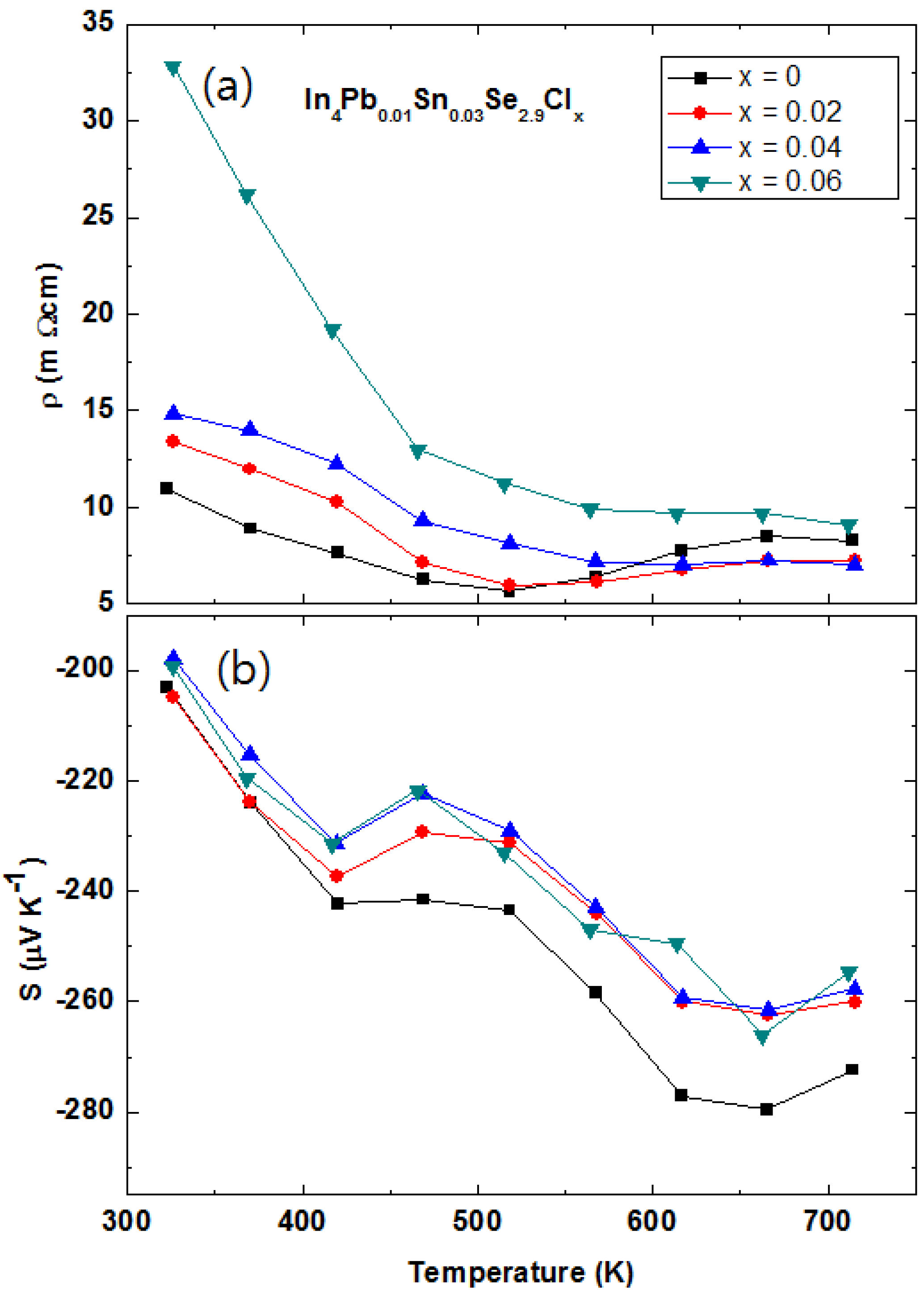
The temperature dependent electrical resistivity of the polycrystalline In
4Pb
0.01Sn
0.03Se
2.9Cl
x (
x = 0.02, 0.04, and 0.06) polycrystalline compounds and
x = 0.0 (Ref. [
43]) are presented in
Figure 23a. The electrical resistivity of Cl-doped compounds shows the semiconducting behavior in the measured temperature range. The increasing electrical resistivity with increasing Cl doping shows a similar behavior as In
4Se
2.7Cl
x [
31].
Figure 23.
Temperature-dependent electrical resistivity ρ
(T) (
a) and Seebeck coefficient
S(T) (
b) of the In
4Pb
0.01Sn
0.03Se
2.9Cl
x (
x = 0.0, 0.02, 0.04, and 0.06) polycrystalline compounds [
48].
Figure 23.
Temperature-dependent electrical resistivity ρ
(T) (
a) and Seebeck coefficient
S(T) (
b) of the In
4Pb
0.01Sn
0.03Se
2.9Cl
x (
x = 0.0, 0.02, 0.04, and 0.06) polycrystalline compounds [
48].
From the Hall resistivity ρ
xy and electrical resistivity ρ measurements, we obtain the effective carrier concentration
nH and Hall mobility μ
H, which are listed in
Table 10. The carrier concentration of the In
4Pb
0.01Sn
0.03Se
2.9Cl
x (
x = 0.02) compound shows the value of 1.58 times higher than the one of pristine In
4Pb
0.01Sn
0.03Se
2.9 polycrystalline compound. The carrier concentration does not increase with Cl doping for
x = 0.04 and 0.06, implying the solubility limit of the compounds as in the case of the polycrystalline In
4Se
2.7Cl
x polycrystalline compounds (
x = 0~0.05) [
31].
Table 10.
The Hall carrier concentration
nH, electrical resistivity ρ, Hall mobility μ
H, negative Seebeck coefficient −|
S|, and effective mass of carrier
m* of the In
4Pb
0.01Sn
0.03Se
2.9Cl
x (
x = 0, 0.02, 0.04, and 0.06) polycrystalline compounds at 320 K [
48].
Table 10.
The Hall carrier concentration nH, electrical resistivity ρ, Hall mobility μH, negative Seebeck coefficient −|S|, and effective mass of carrier m* of the In4Pb0.01Sn0.03Se2.9Clx (x = 0, 0.02, 0.04, and 0.06) polycrystalline compounds at 320 K [48].
| x | nH (×1018 cm−3) | ρ (mΩ·cm) | μH (cm2·V−1·s−1) | −S (μV/K) | m* (me) |
|---|
| 0.00 | 2.67 | 10.9 | 214 | 203 | 0.18 |
| 0.02 | 4.22 | 13.4 | 111 | 205 | 0.25 |
| 0.04 | 4.09 | 14.9 | 103 | 198 | 0.24 |
| 0.06 | 3.99 | 32.9 | 48 | 199 | 0.23 |
The Hall mobilities of the In
4Pb
0.01Sn
0.03Se
2.9Cl
x polycrystalline compounds are decreased with increasing Cl-doping. In contrast with the result of In
4Se
3−xCl
0.03 single crystal [
29], the polycrystalline compounds of In
4Se
2.7Cl
x [
31] and In
4Pb
0.01Sn
0.03Se
2.9Cl
x decreased the Hall mobility by increasing the Cl-doping. It implies that the Hall mobility of polycrystalline In
4Se
3 is decreased by the excess Cl-impurity scattering at the grain boundary. However, the CuBr-doped In
4Se
2.5 polycrystal shows the increased Hall mobility [
50].
The increase of Hall mobility in bulk crystalline materials is caused by the enhancement of crystallinity in chlorine doped In
4Se
3−xCl
0.03 single crystal [
29]. For example, the x-ray diffraction patterns for the cross-sectional planes of crystalline ingots show well aligned crystal orientation. However, for polycrystalline materials, the Hall mobility of chlorine doped samples is decreased with increasing chlorine doping concentration [
29]. This implies that the chlorine itself acts as scattering center of carriers but it helps to enhance crystallinity during crystal growth. The doped chlorine can increase Hall carrier density, but excess chlorine can precipitate at the grain boundaries, resulting in the decrease of Hall mobility. On the other hand, the single crystalline materials have less effect on grain boundary, thereby the enhanced crystallinity can increase Hall mobility of carriers.
The temperature dependent Seebeck coefficient
S(
T) of the polycrystalline In
4Pb
0.01Sn
0.03Se
2.9Cl
x (
x = 0.02, 0.04, and 0.06) compounds are decreased with Cl-doping as compared with
x = 0.0 as shown
Figure 23b. From the Hall carrier concentration and the measured Seebeck coefficient, the calculated effective masses of the carriers are listed in
Table 10. The effective mass of carrier of
x = 0.02 sample is obviously increased as compared the one of
x = 0.0, even though the Cl-doping dependence is not clear. The increased effective mass of carrier indicates less dispersive electron band than the non-Cl-doped sample. From the effective thermal band gap relation,
Eg = 2eSmaxTmax [
46], we can estimate the band gap as 0.372 eV (
x = 0.0) [
40] and 0.347 eV (
x = 0.04). The Cl-doping on the In
4Pb
0.01Sn
0.03Se
2.9Cl
x compounds induces the less dispersive and decreased band gap than those of the In
4Pb
0.01Sn
0.03Se
2.9 compound.
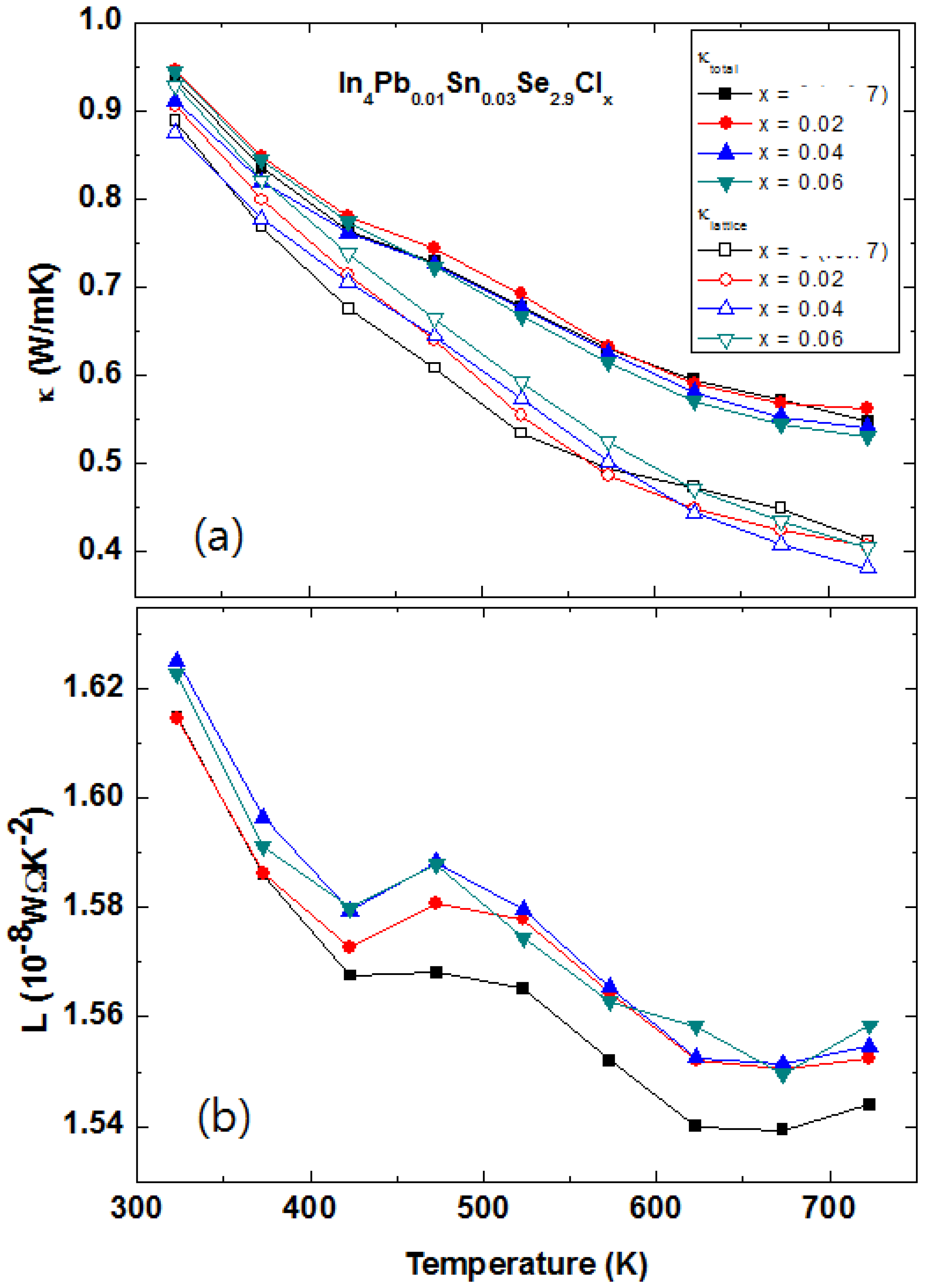
The total thermal conductivities of the polycrystalline In
4Pb
0.01Sn
0.03Se
2.9Cl
x (
x = 0, 0.02, 0.04 and 0.06) polycrystalline compounds are presented in
Figure 24a. The thermal conductivities of (
x = 0.0, 0.02, 0.04, and 0.06) are decreased with increasing temperature. This conventional 1/
T behavior is mainly caused by an acoustic phonon contribution for the thermal transport. There is no systematic change of the κ
(T) with respect to Cl-doping concentration. In general, the total thermal conductivity κ is composed of electrical κ
el and lattice thermal conductivity κ
ph. The electronic thermal conductivity κ
el can be calculated by the Wiedemann-Franz law κ
el =
L0σ
T, where
L0, σ, and
T are the Lorenz number, electrical conductivity, and absolute temperature, respectively. In usual cases, the Lorenz number is written as:
Figure 24.
Temperature-dependent total thermal conductivity κ
tot (closed symbols), lattice thermal conductivity κ
ph (
a), and Lorenz number
L(
T) (
b) of the In
4Pb
0.01Sn
0.03Se
2.9Cl
x (
x = 0.0, 0.02, 0.04, and 0.06) polycrystalline compounds [
48].
Figure 24.
Temperature-dependent total thermal conductivity κ
tot (closed symbols), lattice thermal conductivity κ
ph (
a), and Lorenz number
L(
T) (
b) of the In
4Pb
0.01Sn
0.03Se
2.9Cl
x (
x = 0.0, 0.02, 0.04, and 0.06) polycrystalline compounds [
48].
However, the Lorenz number is incorrect in correlated metal and many degenerated semiconductors. In order to get a more reliable Lorenz number, we calculated the Lorenz number by using the following equation:
where
r is the scattering parameter, η =
EF/kBT is the reduced Fermi energy, and
Fn(η
) is the
n-th order Fermi integral given by:
For most cases, the scattering parameter for acoustic phonon scattering is
r =
1/2. When we fit the measured Seebeck coefficient to the following equation with a free parameter η, we can get the Fermi integral η:
By using the Fermi integral, the calculated temperature dependent Lorenz numbers of In
4Pb
0.01Sn
0.03Se
2.9Cl
x (
x = 0.0, 0.02, 0.04, and 0.06) are shown in
Figure 24b. The calculated temperature dependent Lorenz number is lower than the conventional Lorenz number
L0 = 2.45 × 10
−8 W·Ω·K
−2. The low Lorenz numbers indicate that the electrical contribution for thermal transport is lower than conventional metals. Using the calculated Lorenz number and electrical resistivity, we can obtain the lattice thermal conductivity by subtracting the electrical thermal conductivity from the total thermal conductivity as shown
Figure 24a (open symbols). The change of lattice thermal conductivity with respect to chlorine doping concentration of In
4Pb
0.01Sn
0.03Se
2.9Cl
x (
x = 0.0, 0.02, 0.04, and 0.06) polycrystals is not obvious. The similar thermal conductivity can be explained by the similarity of crystal structure and phonon dispersion relation between In
4Se
3 and InSe [
51].
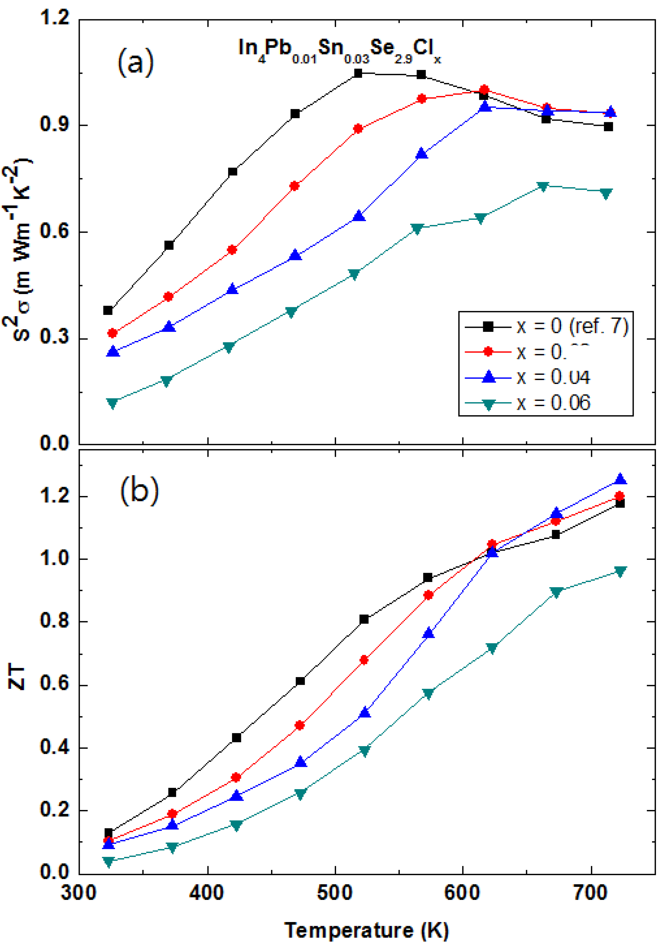
Figure 25a shows the temperature dependent power factor
S2σ of the polycrystalline In
4Pb
0.01Sn
0.03Se
2.9Cl
x (
x = 0.0, 0.02, 0.04, and 0.06) compounds. The decreased power factor with increasing Cl-doping is mainly caused by the decreased Hall mobility near room- and mid-temperature range. On the other hand, the slightly increased power factors of
x = 0.02 and 0.04 are obtained near 723 K. The compound of
x = 0.06 shows a decreased power factor than the other samples (
x = 0.0, 0.02, and 0.04) implying that the InSe phase separation is not good for increasing power factor in the In
4Se
3 phase.
The
ZT values of the polycrystalline In
4Pb
0.01Sn
0.03Se
2.9Cl
x (
x = 0.0, 0.02, 0.04, and 0.06) compounds are presented in
Figure 25b. The maximum
ZT of
x = 0.04 reaches up to 1.25 at 723 K, which is slightly increased value as compared with the one of pristine compound
x = 0.0 (
ZT = 1.2). The high
ZT value over a wide temperature range in bulk crystals In
4Se
3−xCl
0.03 (1.53) is caused by the significant increase of Hall mobility, which is attributed from the enhancement of crystallinity by chlorine doping [
29]. Because the polycrystalline In
4Se
2.7Cl
x samples exhibit decreased
ZT (0.67) value with increasing chlorine doping concentration, we believe that further enhancement of
ZT can be possible in the compounds of In
4Pb
0.01Sn
0.03Se
2.9Cl
x for single crystalline form. Therefore, we should investigate the thermoelectric properties of the single crystalline compounds in further research projects.
Figure 25.
Temperature-dependent power factor
S2σ (
a) and
ZT values (
b) of the In
4Pb
0.01Sn
0.03Se
2.9Cl
x (
x = 0.0, 0.02, 0.04 and 0.06) polycrystalline compounds [
48].
Figure 25.
Temperature-dependent power factor
S2σ (
a) and
ZT values (
b) of the In
4Pb
0.01Sn
0.03Se
2.9Cl
x (
x = 0.0, 0.02, 0.04 and 0.06) polycrystalline compounds [
48].


